Article

Optoelectronic Properties of Atomically Thin MoxW(1−x)S2 Nanoflakes Probed by Spatially-Resolved Monochromated EELS

1
Instituto de Nanociencia y Materiales de Aragon (INMA), CSIC-U. de Zaragoza, Calle Pedro Cerbuna 12, 50009 Zaragoza, Spain
2
Laboratorio de Microscopias Avanzadas, Universidad de Zaragoza, Calle Mariano Esquillor, 50018 Zaragoza, Spain
3
National Institute of Advanced Industrial Science and Technology (AIST), Tsukuba 305-8565, Japan
4
The Institute of Scientific and Industrial Research (ISIR-SANKEN), Osaka University, Osaka 567-0047, Japan
5
ARAID Fundation, 50018 Zaragoza, Spain
*
Author to whom correspondence should be addressed.
Nanomaterials 2021, 11(12), 3218; https://0-doi-org.brum.beds.ac.uk/10.3390/nano11123218
Submission received: 3 October 2021 / Revised: 10 November 2021 / Accepted: 16 November 2021 / Published: 26 November 2021
(This article belongs to the Special Issue Luminescence Properties of Nanomaterials and Nanocomposites)

Abstract

:
Band gap engineering of atomically thin two-dimensional (2D) materials has attracted a huge amount of interest as a key aspect to the application of these materials in nanooptoelectronics and nanophotonics. Low-loss electron energy loss spectroscopy has been employed to perform a direct measurement of the band gap in atomically thin Mo x W ( 1 x ) S 2 nanoflakes. The results show a bowing effect with the alloying degree, which fits previous studies focused on excitonic transitions. Additional properties regarding the Van Hove singularities in the density of states of these materials, as well as high energy excitonic transition, have been analysed as well.

1. Introduction

Atomically thin two-dimensional (2D) materials have been on the spotlight of modern research ever since the isolation of graphene in 2004 [1]. This ample interest comes for the most part from their appealing electronic, thermal and mechanic properties among others; as well as a vast number of potential and real applications [2,3,4]. Within 2D materials, layered transition metal dichalcogenide (TMD) semiconductors of the TX 2 type (with T being a transition metal and X being a chalcogen) have attracted an important amount of research interest [5,6], given their interesting properties when it comes to optoelectronics [7,8,9,10,11], excitonics [11,12,13,14,15] and catalysis [16,17,18,19,20,21,22,23,24].
Concerning the electronic properties of 2D materials, tunable band gaps seem to have become crucial for the further development of electronic applications [24,25,26,27,28,29,30,31,32,33]. Most available 2D materials offer limited and rigid band gap values to work with (5.8 eV for monolayer BN [34,35,36,37] and 0 eV for monolayer graphene [38], for instance) and offer a limited versatility for electronic applications. TMDs offer a wider range of applications in this realm. Diverse approaches have been tried for band gap tuning in 2D materials, and TMDS have been no exception. Band gap tuning of 2D TMDs by means of functionalisation [30,39,40], dielectric screening [41], doping [42,43,44], straining [29,45] and phase engineering [46,47], alloying [48,49,50,51,52,53], as well as combinations of these methods [26], have been on the spotlight of 2D material research.
Alloying of materials with different band gaps has been a commonly used technique for band gap tuning in bulk materials. when it comes to 2D TMDs, even though bulk TMD alloys have existed for decades now, a wide array of 2D TMD alloys have been synthesised in the past decade [54], thanks to the development in synthesis techniques such as chemical vapor deposition [32], physical vapor deposition [55], chalcogen exchange [32] and colloidal solution synthesis [51,52]. Even so, only a small number of alloys has been achieved so far; most of them ternary alloys based on Mo, W, S, Se and Te [16,24,32,51,52,55,56,57,58,59,60], although new alloys with different transition metals have also been achieved [33,58,61,62], as well as quaternary alloys [17,63,64,65,66]. Novel optoelectronic applications have arisen from these new materials [66,67,68,69].
Within these alloys, Mo x W ( 1 x ) S 2 alloys have received an important amount of research interest, due to their being the first 2D TMD alloy to ever be synthesised and characterised [48,70,71], but also because of its various potential application regarding optoelectronics [53,72,73], hydrogen evolution reaction [23,74] and laser optics [75]. This has prompted an important amount of research efforts with the objective of characterising and modelling the behaviour of these alloys, especially when it comes to their optoelectronic properties [25,48,70,76,77,78].
However, the studies concerning the band gap of Mo x W ( 1 x ) S 2 alloys are based on photoluminescence (PL) and scanning tunneling spectroscopy (STS) experiments, and have only focused on the low energy empty states of these materials [16,48,77,78,79]. These are related to the band gap of a specific material, but they do not conform a direct measurement of said band gap, even though it has been discussed as such in the literature [80]. In this sense, one of the main focus points of this study is performing a direct measurement of the band gap for the different alloys presented.
This study aims as well for a detailed and direct characterization of optoelectronic properties in atomically thin Mo x W ( 1 x ) S 2 alloys as a function of their alloying degree. Additionally, STEM-EELS offers the possibility to perform these studies at the nanoscale while being able to calculate the thickness of the measured sample, therefore comparing the results obtained not just by the alloying degree of regions being sampled but also their number of layers.

2. Methods

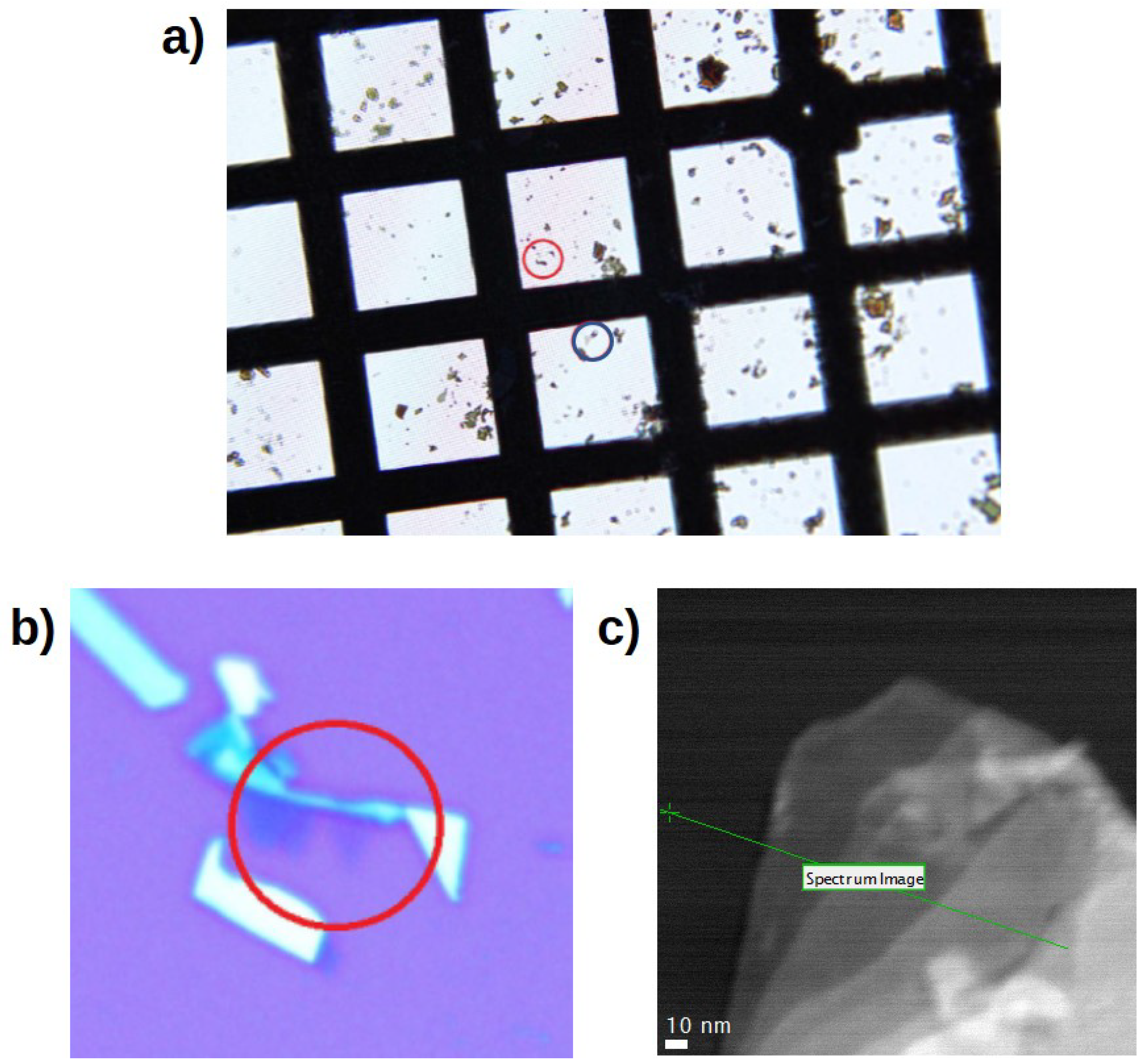
2.1. Sample Preparation

Mo x W ( 1 x ) S 2 single crystals have been synthesised by means of chemical vapor transport (CVT), as done in previous works [48,70,71,72,81]. Different precursor ratios have been used to obtain different final alloying degrees. After synthesis, the crystals have been mechanically exfoliated, and the alloy flakes have been transferred to TEM grids.

2.2. Sample Characterisation

Once the samples have been prepared, for each one of them areas presenting a low number of layers have been identified and selected. This identification has been performed by means of optical and low-magnification TEM images such as the ones presented in Appendix A. These areas were later identified for subsequent spectroscopic measurements.
Initial characterisation of the different alloys has been performed using two STEMs, a JEM-ARM200F with a CEOS corrector was operated at 80 kV and a Jem-2100F with a DELTA corrector was operated at 60 kV. All monochromated STEM-EELS studies performed for this study has been carried out using a ThermoFischer Titan probe-corrected microscope working at 80 KV. The microscope is equipped with a Gatan Energy Filter (GIF) Tridiem 866 ERS and a monochromator that combined grant a resolution in energy of about ∼180 meV.
Initial HRSTEM characterization has been performed in alloy monolayers. Figure 1 shows three different HRSTEM high-angle annular dark field (HAADF) micrographs corresponding to three monolayers of MoS 2 , Mo 0.5 W 0.5 S 2 and WS 2 samples, respectively. As it can be seen in these micrographs, as well as previous works [48,71], these Mo x W ( 1 x ) S 2 alloys present a hexagonal layered structure, corresponding to the 2H phase in their precursors MoS 2 and WS 2 .
The alloying degree of these alloys has been directly determined from the proportion of Mo and W in these micrographs, deduced from the different contrasts among Mo, W and S atoms due to their difference in atomic number [71]. Five Mo x W ( 1 x ) S 2 samples were used in this study; each one with a different alloying degree: x = 0, 0.3, 0.5, 0.7 and 1, respectively.
For each alloy, In each few-layer region of interest, HAADF-STEM micrographs have been taken to determine where to perform the STEM-EELS studies. In these locations, low-loss EEL spectra were recorded using the spectrum-line mode [82]. An HAADF-STEM intensity profile was recorded simultaneously as well. An example of a spectrum-line scan, as well as its corresponding HAADF-STEM intensity profile, is shown in Figure 2.

2.3. Data Treatment

For each one of the spectrum profiles, several spectra have been integrated. On the one hand, 6 spectra have been integrated right below the onset for the HAADF-STEM intensity. These integrated spectra account for the aloof spectroscopic analysis needed for band gap estimation. On the other hand, regions have been identified along the profile where the intensity plateaus. This, along with their corresponding HAADF-STEM micrograph, has served to identify regions in the intensity profile where thickness is constant. In these regions, spectra have been integrated over a window between 10 and 30 nm wide, integrating 4 to 6 spectra to improve the signal-to-noise ratio (SNR). Spectra close to the edges of the different plateaus have purposefully been taken out of the integrated spectra to minimise plasmonic contributions, as they have been seen for MoS 2 [83,84,85]. A depiction of these flat areas can be seen in Figure 2. For every integrated spectrum, the thickness of the spectra has been estimated using the log-ratio method [86]. Further insight on this estimation, can be seen in Appendix A.
For each integrated spectrum, after zero loss peak (ZLP) extraction, two different types of analysis have been performed in each spectrum, focusing respectively on the band gap of the sample on one hand and on the rest of optoelectronic features on the other hand. No analyses could be performed on the nature of the A and B excitonic peaks due to the energy resolution in these works not being able to discern both features, but given these two excitonic features are the main influence on the band gap of the samples, it is sensible to assume their behaviour as a function of alloying degree will be similar to that of the band gap.
Regarding the band gap analysis, focused in the spectral region between 1.5 and 2 eV, initially a Richardson-Lucy deconvolution has been performed in order to increase the SNR in the spectra [35,87,88]. The deconvoluted spectra have been linearly fitted over a window of 0.1 eV situated in the band gap region. The x-intercept value of said fit has been taken as the measured band gap value of the sample in the region [35,88].
As for the rest of the features in the low-loss EEL spectra, a triple Gaussian fit of each spectrum has been performed in an energy window between 2.5 and 6 eV in order to determine the values of the C excitonic feature as well as the α and β Van Hove features (see next section). The full-width at half maximum of the Gaussian fit related to the β Van Hove features has been constrained in order to keep it coherent with the data analysed, as it is discussed in Appendix A. The presence of an excitonic feature in this spectral region is discussed in Appendix A as well.

3. Results and Discussion

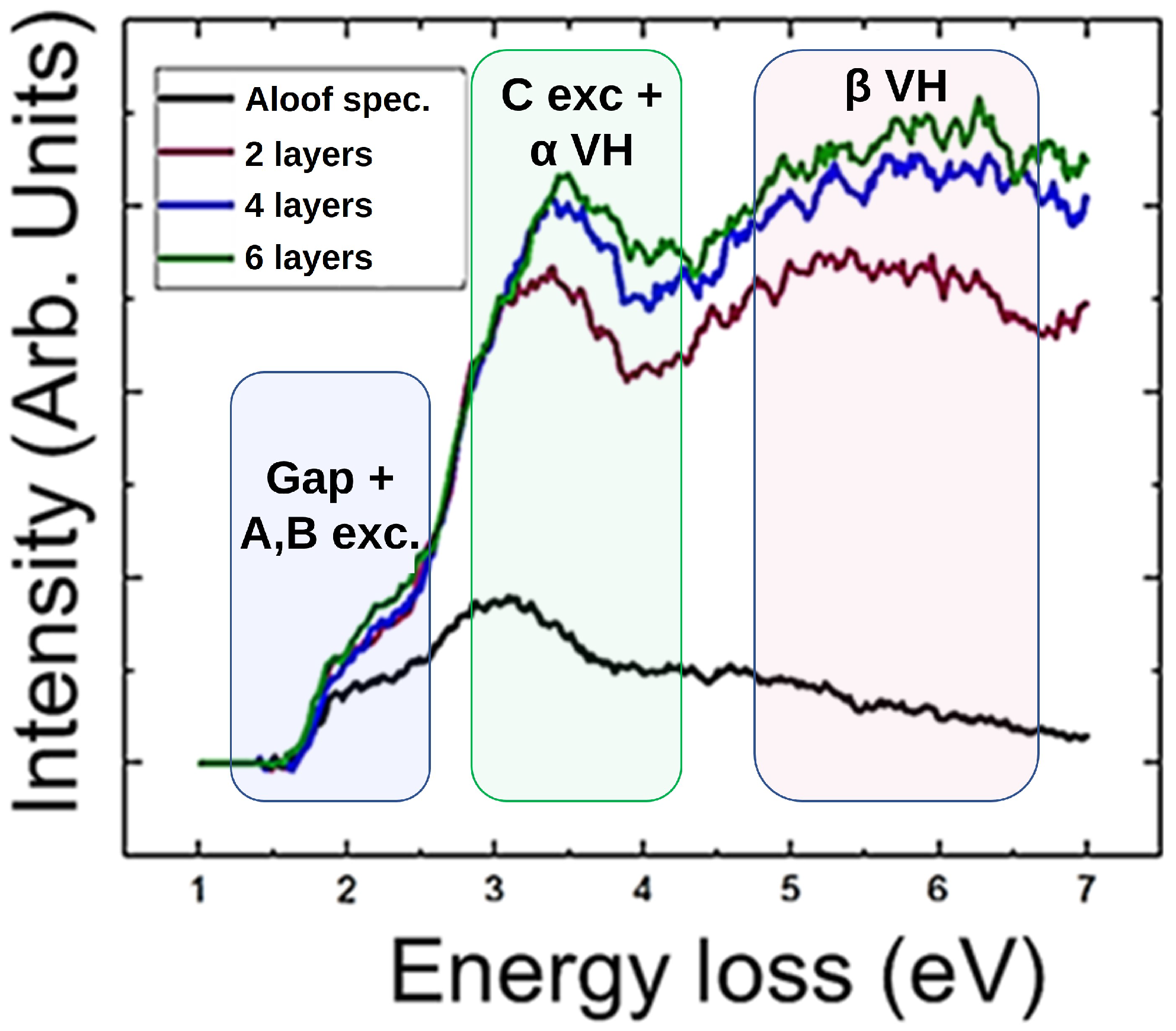
3.1. Integrated EEL Spectra; Features and Interpretation
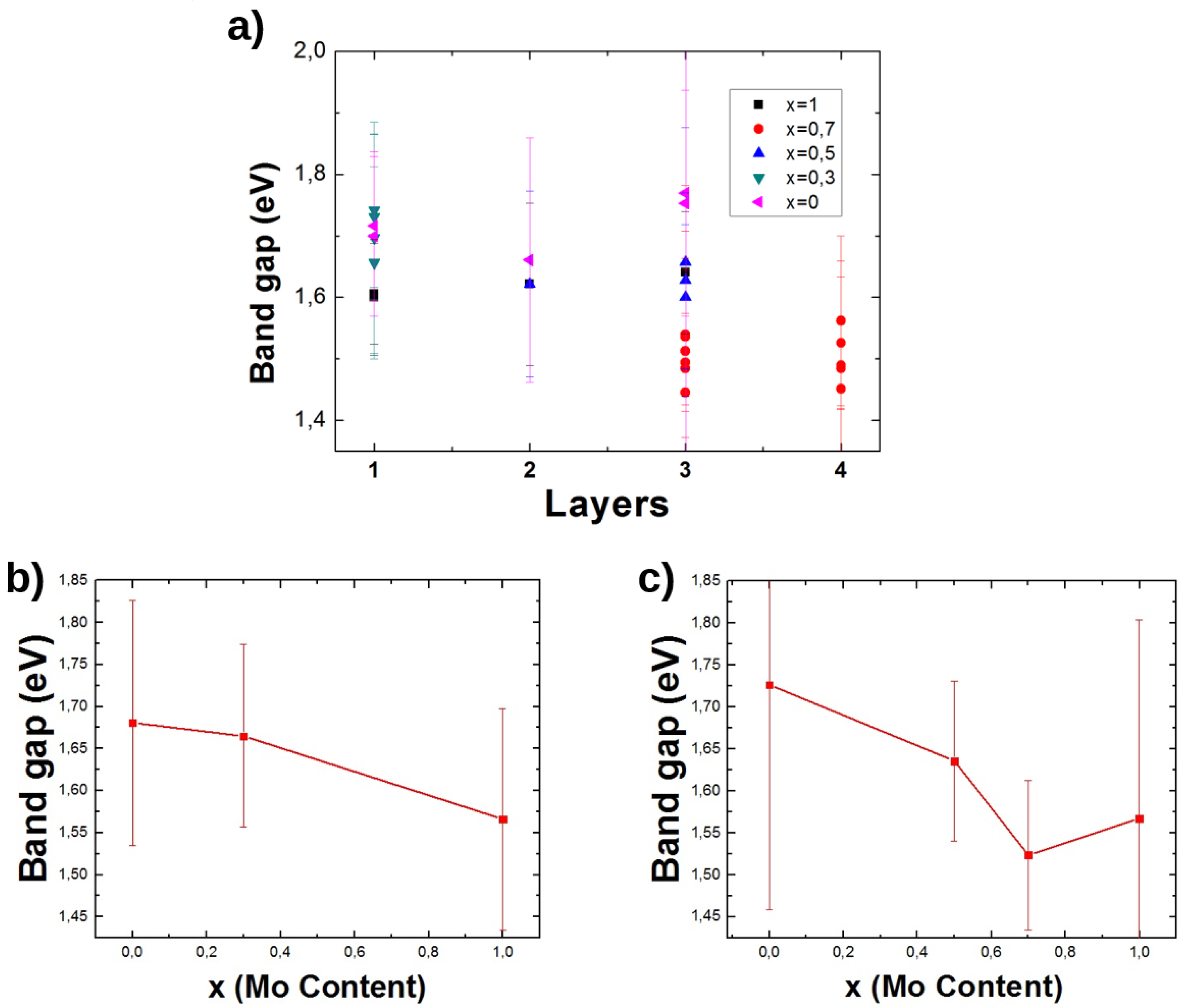
In order to better interpret the gathered EEL spectra in these alloys, it is important to delve deeper into their optoelectronic properties. The main phenomena that rules over the electronic band structure of the samples, and in turn its band gap, are excitons. The dielectric confinement in TMDs incites the formation of highly stable, strongly bound excitons at low energies [12,58]. Due to high spin-orbit coupling, there is a spin splitting in the valence band, giving rise to two excitonic features in the EEL spectra at low energy, called A and B respectively. A third excitonic feature, called C, has been reported in the literature both from an experimental and a theoretical point of view [89,90,91]. As it can be seen in Appendix A, the data gathered in these works fits the presence of this excitonic feature in these samples, and its analysis is included in the optoelectronic characterisation of said samples.
An additional property of interest in these materials when it comes to their optoelectronic properties is the existence of discontinuities in their density of states (DOS). This kind of discontinuities are called Van Hove singularities, and their effect can be seen in the EEL spectra as features around this discontinuity in the DOS, since these discontinuities serve as triggers for transitions at a very specific energy. In the case of the materials that we study in these works, they both exhibit two distinct Van Hove singularities, which in turn produce two separate features in the EEL spectra, denominated as α and β respectively. These features have been previously identified in EEL spectra for MoS 2 [92,93,94].
It is important to notice that the intensity in the β Van hove region for the aloof spectra is noticeably lower in comparison with the rest of the spectra. Our hypothesis for this behaviour is that it could be likely related to some volume/bulk (even for the case of monolayer case) contribution on these involved electronic features. For instance, similar behavior has been observed in the case of single-walled boron nitride nanotubes [35].
Figure 3 shows the integrated spectra from the regions highlighted in Figure 2, along with the regions of interest with respect to these studies.
As it can be seen, the C excitonic feature and the α van Hove feature appear to be overlapped on the same energy window. However, it has been proven (see Appendix A) that both features can be distinguished from one another.

3.2. Band Gap

The results concerning the band gap measurements as a function of Mo content (alloying degree) can be seen in Figure 4.
These results represent the first direct measurement of the optical gap of such nanomaterials to the best of our knowledge. Generally speaking, the preferred technique of choice for the measurement the optical gap of a bulk material is optical absorption [95], which probes the frequency dependence of the imaginary term in the dielectric function ε ω [96]. On the other hand, EEL spectra are proportional to the energy loss function I m 1 / ε ω [97]. In bulk materials and penetrating geometry (when the electron is going through the sample), provided we neglect surface loss contributions, this term for the energy loss function can be expressed as:
I m 1 / ε ω = ε 2 / ε 1 2 + ε 2 2
where ε 1 and ε 2 are the real and imaginary parts of the dielectric function, which Kramers-Kronig transformations allow to determine from the measured energy-loss function [97,98]. However, this is not the case for thin 2D materials, where the surface effects are much more prominent.
One of the many benefits of STEM-EELS is that it allows a different acquisition mode, non-penetrating “aloof spectroscopy” [99]. In this type of spectroscopy, where the electron beam is set at a grazing position from the nanostructure, it is possible to use the continuous dielectric model (CDM) to delve into the optical responses using EELS [35,88,100,101,102,103,104,105]. It has been shown that, for different nanostructures, in aloof EELS the spectrum is a weighted sum of the imaginary parts of the multipolar polarizabilities γ [104,106]. Provided that few-layer TMD flakes can be considered in the strong-coupling regime of the CDM, the imaginary part of the polarizability can be written for a slab as:
I m ( γ ( ω ) ) = ( I m ( ε ( ω ) 1 / ε ( ω ) ) )
where ε and ε are the components of the dielectric tensor of an alloy sheet that are perpendicular and parallel to the anisotropy axis, respectively.
In the case of MoS 2 and WS 2 , it has been previously studied that the response of ε begins at about 3 eV, therefore it is possible to say that, below this energy, the energy loss function is proportional to ε [103,104,106]. This is what has allowed for the direct measurement of the optical band gap in these samples, which has been taken as the inset of the energy loss ), as it has been previously done for the case of boron nitride nanotubes [88].
Much like previous works on the excitonic behaviour of these alloys [48,57,77,78,79,80,107], as well as recent modelling [25], the results on the value of the the band gap for different alloying degrees show a bowing effect as a function of the alloying degree. This bowing effect has been found to originate from the different variation of the valence and conduction bands with the alloying degrees. Density functional theory (DFT) calculations have shown that, whereas the valence band variates linearly, the conduction band varies non-linearly with the alloying degree [48].
The band gap values that have been found are slightly lower than those shown in the literature for photoluminescence (PL) studies, but it is coherent, since generally the value given for the band gap for these materials is the value of the A exciton peak, which dominates the band gap but is slightly higher in energy. It has not been possible, however, to discern if the band gap shifts in a particular way with the number of layers for each individual alloy. Discussion on this topic can be seen in Appendix A.

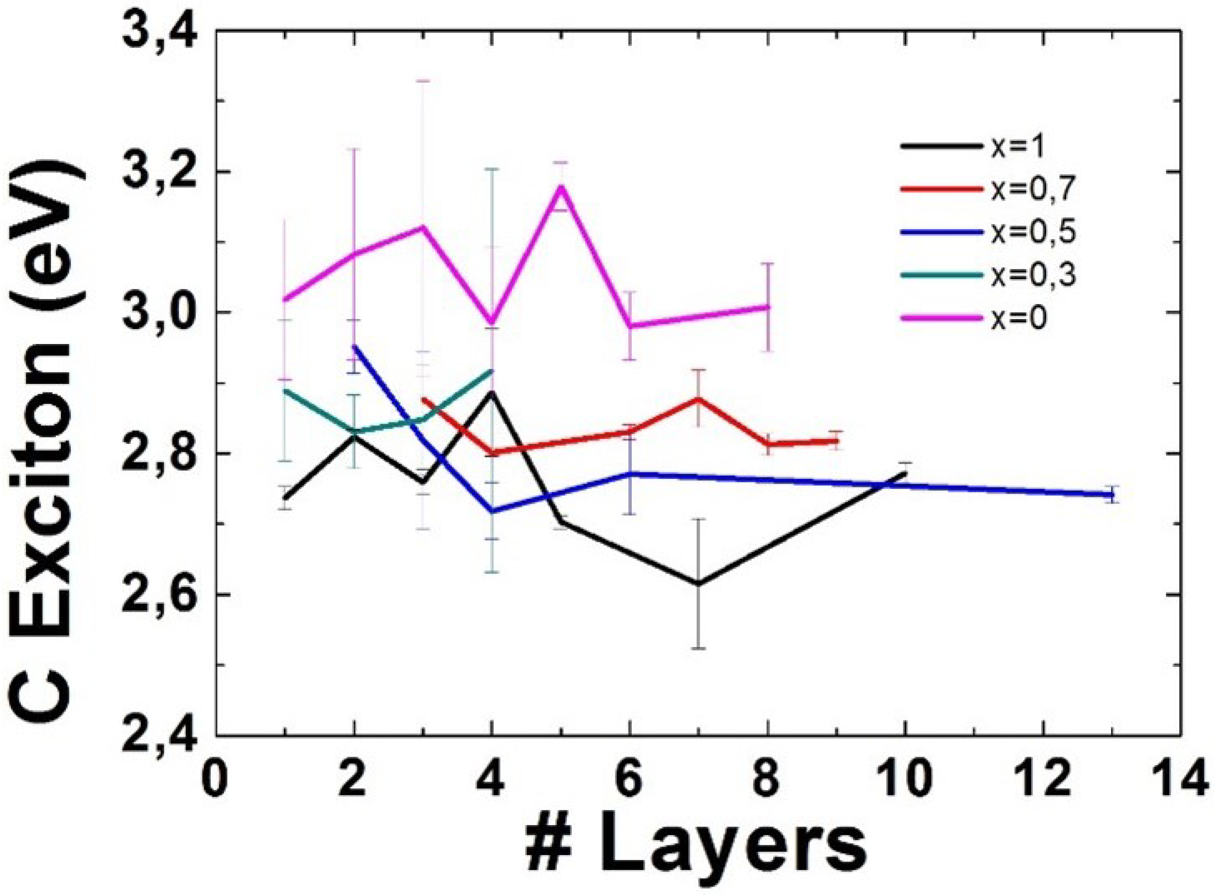
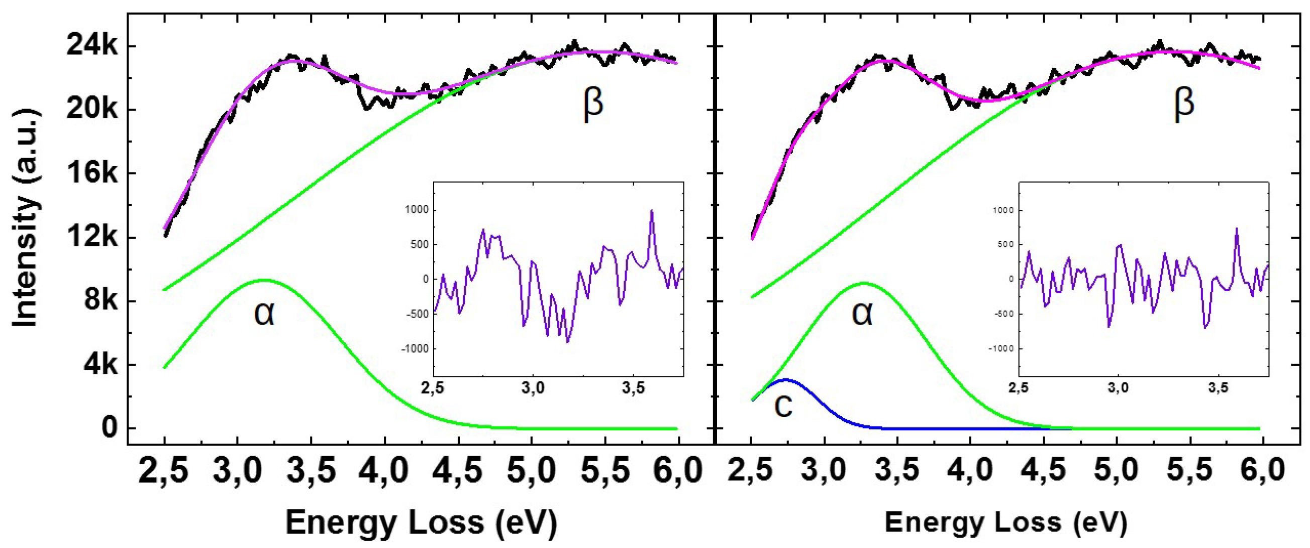
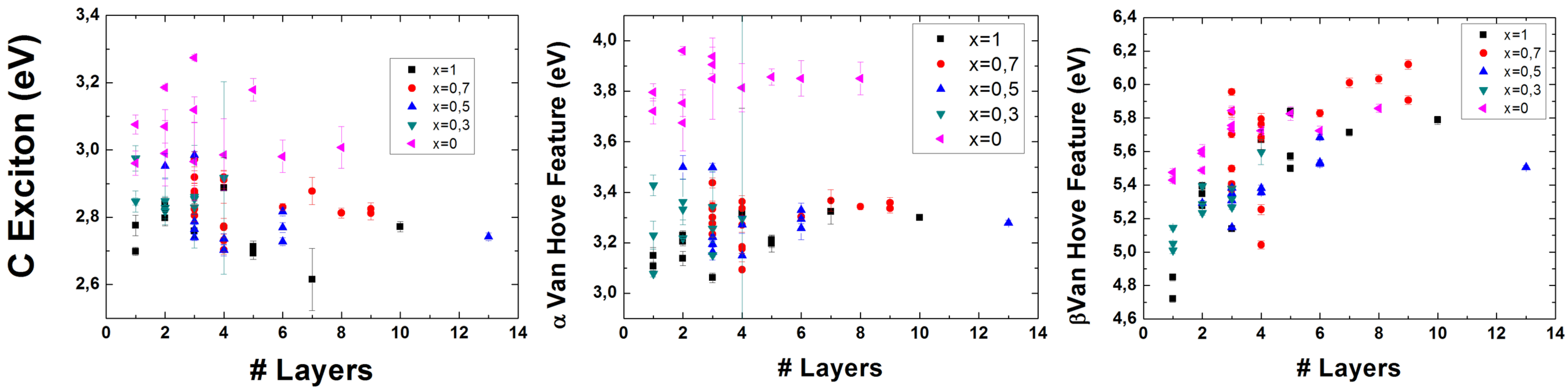
3.3. C Excitonic Feature

The average value of the C excitonic features for each number of layers and each alloying degree can be seen in Figure 5. The results show a slight tendency from the C excitonic features to decrease with the number of layers for each specific alloying degree. This behaviour is more evident for some of alloying degrees. Regarding the behaviour of the C exciton with respect to the alloying degree, the position of these C excitonic features seems to decrease with the alloying degree as well. It is worth to remark the most notable difference in these values among alloying degrees, which occurs for WS 2 .

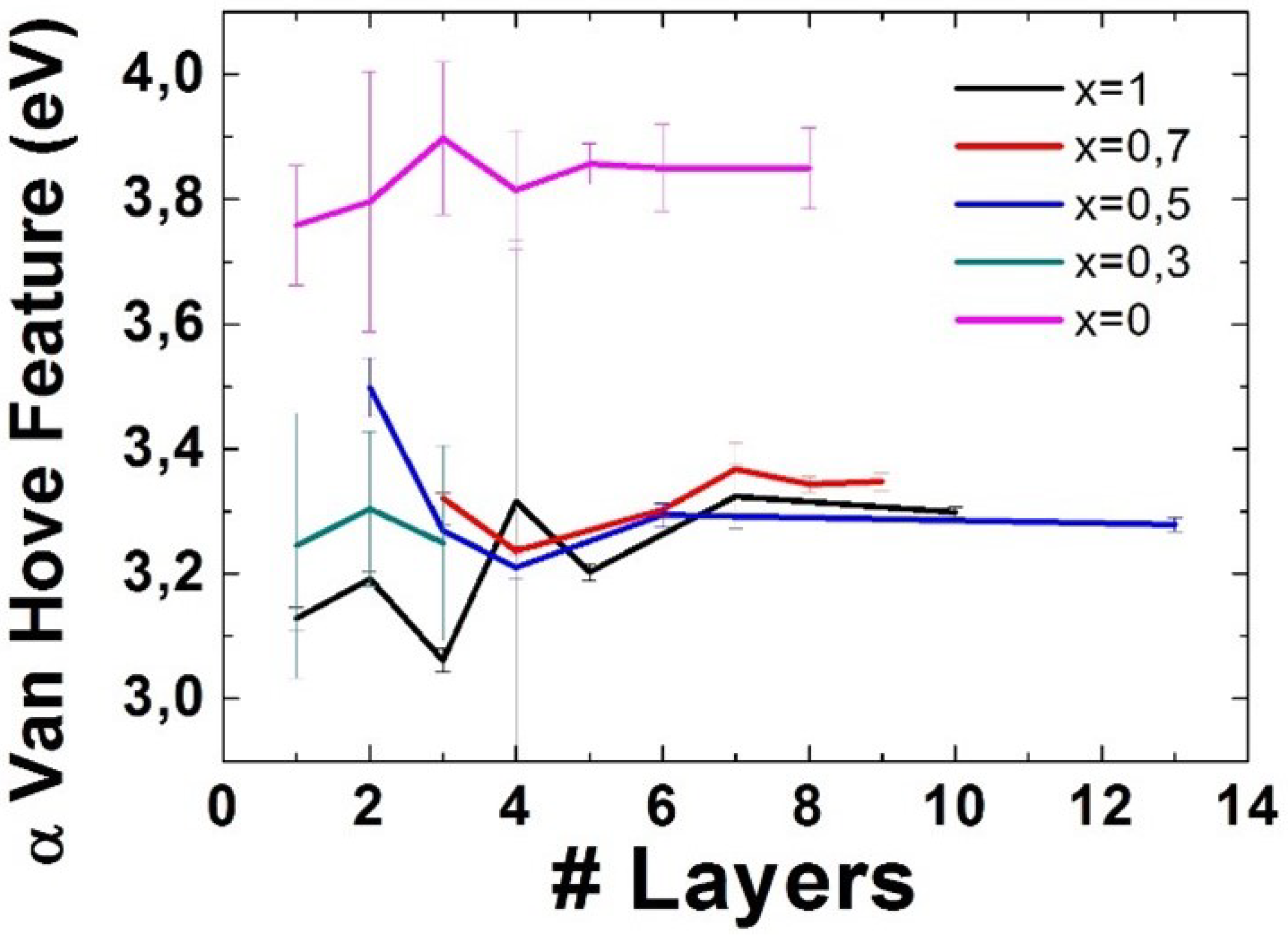
3.4. Van Hove Features

Results regarding the position of the Gaussian fit assigned to the α Van Hove feature are shown in Figure 6.
Even though the results for low number of layers show a small decrease for x = 0.5, there is a general, albeit small, increase of the α Van Hove feature with the number of layers. As for the variation of this feature with the alloying degree, it seems to go down as the alloying degree goes up. Once again, the great difference in the value for this feature between WS 2 and the rest of the alloys is also worth mentioning.
Finally, results concerning the behaviour of the position of the Gaussian fit assigned to the β Van Hove feature can be found in Figure 7.
Results show a very clear increase in the position of this feature as the number of layers increases. However, it is not as easy to discern the behaviour of this feature as a function of the alloying degree of the material. This can be due to the analytic constrains set for this fit to keep the rest of the analysis consistent (see Appendix A). The raw results on each individual measurement of all features in the low-loss EELS region can be seen in Appendix A as well.

4. Conclusions

A direct measurement of the optical band gap of several Mo x W ( 1 x ) S 2 alloys is reported by means of non-penetrative low-loss EELS analyses. This band gap oscillates between 1.5 (reached at x = 0.7) and 1.72 eV (reached at x = 0), showing a bowing effect that is coherent with both previous experimental and modelled results [48]. The A and B excitons are expected to follow the same behaviour.
The behaviour of the C excitonic feature, due to several excitonic transitions shows a slight tendency from the C excitonic features to decrease with the alloying degree, and within the same alloying degree it seems to have a slight decreasing tendency as the number of layers goes up.
As for the α and β van Hove Features, a decreasing tendency can be found for the α feature as the alloying degree increases, whereas no clear tendency can be found for the β feature. As for the behaviour with respect to the number of layers, they both seem to increase in energy with thickness, albeit not in a uniform way.
This detailed optoelectronic characterisation of an atomically thin tunable sample composed of transition metal dichalcogenides will be of great use for future nanooptoelectronic and nanophotonic applications of these materials.

Author Contributions

Conceptualization, R.A. and K.S.; methodology, M.P.-F. and R.A.; validation, M.P.-F. and R.A.; formal analysis, M.P.-F. and R.A.; investigation, M.P.-F., Y.-C.L., K.S. and R.A.; data curation, M.P.-F. and R.A.; writing—original draft preparation, M.P.-F. and R.A.; writing—review and editing, M.P.-F., Y.-C.L., K.S. and R.A.; visualization, M.P.-F. and R.A.; supervision, R.A.; project administration, R.A.; funding acquisition, R.A. All authors have read and agreed to the published version of the manuscript.

Funding

Research supported by the Spanish MICINN (PID2019-104739GB-100/AEI/10.13039/ 501100011033), Government of Aragon (project DGA E13-20R) and European Union H2020 programs “ESTEEM3” (823717), Graphene Flagship (881603), JST-CREST (JPMJCR20B1, JPMJCR20B5, JPMJCR1993) and JSPS A3 Foresight Program.

Data Availability Statement

Data available by request to the corresponding author in this article.

Acknowledgments

This article is dedicated to Dieter Gruen on the occasion of his 99th birthday. We acknowledge useful discussions with L. Wirtz and E. Torun (U. Luxembourg). The STEM-EELS studies were conducted at the Laboratorio de Microscopias Avanzadas LMA, Universidad de Zaragoza, Spain.

Conflicts of Interest

The authors declare no conflict of interest. The funders had no role in the design of the study; in the collection, analyses, or interpretation of data; in the writing of the manuscript, or in the decision to publish the results.

Abbreviations

The following abbreviations are used in this manuscript:
PLPhotoluminescence
HRSTEM   High-resolution scanning transmission electron microscopy
HAADFHigh-angle annular dark field
DFTDensity functional theory
EELSElectron energy loss spectroscopy
STSScanning tunnelling spectroscopy

Appendix A. Additional Information of Interest to These Works

Appendix A.1. Optical Characterisation

Figure A1 shows examples of the optical microscopy and STEM images used to find regions of interest with flakes presenting a few layers in the different alloys. Optical microscopy has been used to identify regions with thin flakes, which have then been identified by means of STEM imaging.
Figure A1. Optical microscopy and STEM characterization of atomically thin regions of interest. (a) Low-mag optical microscopy image showing two regions of interest where particularly thin alloy flakes have been found (red and blue circles, respectively). (b) High-mag optical microscopy image showing the region of interest seen in the red circle of the low-mag image. (c) STEM micrograph of the same alloy flake shown in the optical micrographs.
Nanomaterials 11 03218 g0a1

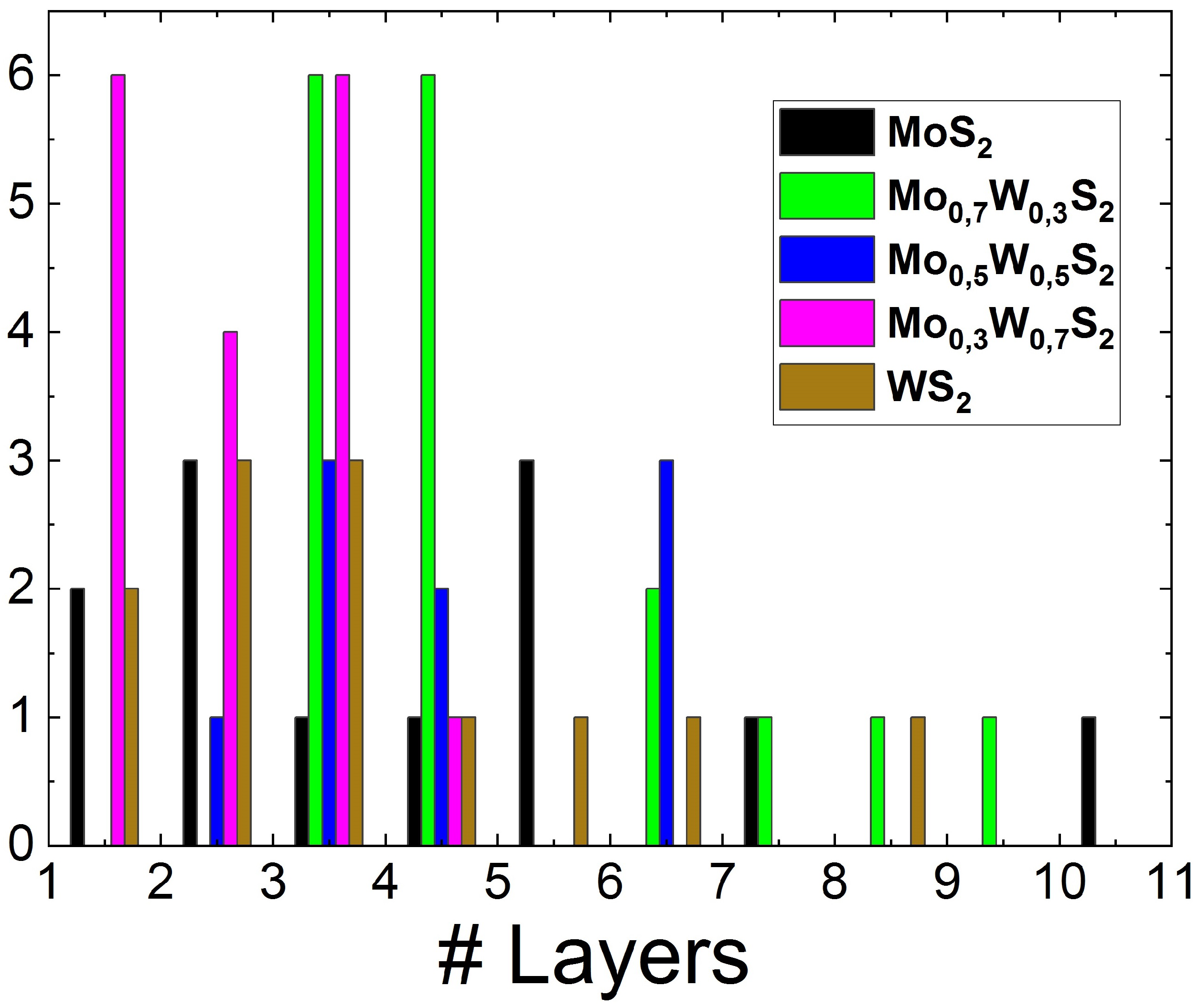
Appendix A.2. Thickness Measurements

A log-ratio method has been employed for the estimation of the thickness in the different alloy flakes. As it has been shown in the literature [86], besides other experimental parameters, this analysis need the effective atomic number Z e f f of the sample. Since the alloy flakes have been shown to be homogeneous in composition, with no clustering of any kind [71], Z e f f can be calculated as a function of the alloying degree and the atomic numbers of Mo, W and S:
Z e f f = x × N M o + 1 x × N W + 2 × N S 3 = x × 42 + 1 x 74 + 2 × 16 3 = 106 32 x 3
By dividing the thickness of the sample by the interlayer distance in MoS 2 and WS 2 (∼6.5 Å [108]), the number of layers of each region has been found. A histogram of the number of measurements performed for each number of layers in each sample can be found in Figure A2.
Figure A2. Histogram showing the number of layers measured for each region of interest in each alloying degree (Mo content).
Nanomaterials 11 03218 g0a2

Appendix A.3. C Exciton and Van Hove Features Analysis

When it comes to the analysis of the C exciton and Van Hove features, a multipeak Gaussian fit approach has been used. However, some restraints have been needed to keep the analysis consistent. Since the feature corresponding to the β Van Hove feature is way more intense than the rest of the features on this window, the behaviour of the Gaussian fit for this feature dominates the analysis on the whole spectral window.
In this sense, we have assumed to have a Gaussian fit for this feature that does not change in width with the number of layers, since there was a clear correlation between the changes in width of the Gaussian fit for the β Van Hove feature and the shift in energy for the other two features in this window. For this, a preliminary analysis has been set in place to gather some insight on the width of this feature, and a second fit has been performed constraining the width of the β Van Hove feature Gaussian to the mean value obtained in the preliminary analysis for that particular alloy.
The fit used also shows the importance of the C excitonic feature, not just from an optoelectronic point of view, but also for the correct analysis of the α van Hove features, since it is evident from the residuals of the analysis that a double Gaussian has trouble correctly fitting the spectra. Figure A3 shows the analysis results for a double Gaussian and a triple Gaussian fit in the energy window from 2.5 to 6 eV.
Figure A3. Comparison of a double and triple Gaussian fit on the 2.5–6 eV energy window for an EEL spectra. Inset: Residuals from the Gaussian fit.
Nanomaterials 11 03218 g0a3

Appendix A.4. Raw Results

The raw results for the values of the bandgap, as well as the average estimation that has been able to be done for the case of monolayer and trilayer samples, can be seen in Figure A4.
Figure A4. Additional results concerning the alloy band gap. (a) Raw values for the band gap measurements in these studies. Error bars are taken as the error in the onset of their corresponding linear regression. (b) Average results for alloy monolayers. (c) Average results for alloy trilayers.
Nanomaterials 11 03218 g0a4
Results show that, even though it is not possible to discern a general behaviour of the band gap with the number of layers, both monolayer and trilayer measurements show the same behaviour as a function of the alloying degree as the general average band gap value.
Figure A5 shows the raw results for the C excitonic feature as well as the α and β van Hove features, from which Figure 5, Figure 6 and Figure 7 have been derived.
Figure A5. Raw results of the analyses in these works. Left to right: C exciton, α and β van Hove features.
Nanomaterials 11 03218 g0a5

References

  1. Novoselov, K.S.; Geim, A.; Morozov, S.V.; Jiang, D.; Zhang, Y.; Dubonos, S.V.; Grigorieva, I.V.; Firsov, A.A. Electric Field Effect in Atomically Thin Carbon Films. Science 2004, 306, 666–669. [Google Scholar] [CrossRef] [Green Version]
  2. Mas-Ballesté, R.; Gómez-Navarro, C.; Gómez-Herrero, J.; Zamora, F. 2D materials: To graphene and beyond. Nanoscale 2011, 3, 20–30. [Google Scholar] [CrossRef] [PubMed]
  3. Lin, Z.; McCreary, A.; Briggs, N.; Subramanian, S.; Zhang, K.; Sun, Y.; Li, X.; Borys, N.J.; Yuan, H.; Fullerton-Shirey, S.K.; et al. 2D materials advances: From large scale synthesis and controlled heterostructures to improved characterization techniques, defects and applications. 2D Mater. 2016, 3, 22002. [Google Scholar] [CrossRef]
  4. Backes, C.; Abdelkader, A.M.; Alonso, C.; Andrieux-Ledier, A.; Arenal, R.; Azpeitia, J.; Balakrishnan, N.; Banszerus, L.; Barjon, J.; Bartali, R.; et al. Production and processing of graphene and related materials. 2D Mater. 2020, 7, 022001. [Google Scholar] [CrossRef]
  5. Chhowalla, M.; Liu, Z.; Zhang, H. Two-dimensional transition metal dichalcogenide (TMD) nanosheets. Chem. Soc. Rev. 2015, 44, 2584–2586. [Google Scholar] [CrossRef] [PubMed]
  6. Manzeli, S.; Ovchinnikov, D.; Pasquier, D.; Yazyev, O.V.; Kis, A. 2D transition metal dichalcogenides. Nat. Rev. Mater. 2017, 2, 139–143. [Google Scholar] [CrossRef]
  7. Yin, Z.; Li, H.; Li, H.; Jiang, L.; Shi, Y.; Sun, Y.; Lu, G.; Zhang, Q.; Chen, X.; Zhang, H. Single-Layer MoS2 Phototransistors. ACS Nano 2012, 6, 74–80. [Google Scholar] [CrossRef] [Green Version]
  8. Splendiani, A.; Sun, L.; Zhang, Y.; Li, T.; Kim, J.; Chim, C.Y.; Galli, G.; Wang, F. Emerging photoluminescence in monolayer MoS2. Nano Lett. 2010, 10, 1271–1275. [Google Scholar] [CrossRef] [PubMed]
  9. Kang, J.; Li, J.; Li, S.S.; Xia, J.B.; Wang, L.W. Electronic structural Moiré pattern effects on MoS2/MoSe2 2D heterostructures. Nano Lett. 2013, 13, 5485–5490. [Google Scholar] [CrossRef]
  10. Mak, K.F.; Lee, C.; Hone, J.; Shan, J.; Heinz, T.F. Atomically thin MoS2: A new direct-gap semiconductor. Phys. Rev. Lett. 2010, 105, 2–5. [Google Scholar] [CrossRef] [Green Version]
  11. Cunningham, P.D.; Hanbicki, A.T.; McCreary, K.M.; Jonker, B.T. Photoinduced Bandgap Renormalization and Exciton Binding Energy Reduction in WS2. ACS Nano 2017, 11, 12601–12608. [Google Scholar] [CrossRef] [PubMed]
  12. Plechinger, G.; Nagler, P.; Arora, A.; Granados Del Águila, A.; Ballottin, M.V.; Frank, T.; Steinleitner, P.; Gmitra, M.; Fabian, J.; Christianen, P.C.; et al. Excitonic Valley Effects in Monolayer WS2 under High Magnetic Fields. Nano Lett. 2016, 16, 7899–7904. [Google Scholar] [CrossRef] [Green Version]
  13. Onga, M.; Zhang, Y.; Ideue, T.; Iwasa, Y. Exciton Hall effect and transport of valley exciton in monolayer MoS2. In SAP-OSA Joint Symposia 2017 Abstracts; Japan Society of Applied Physics, Optical Society of America: Fukuoka, Japan, 2017. [Google Scholar]
  14. Gupta, P.; Dongare, P.D.; Grover, S.; Dubey, S.; Mamgain, H.; Bhattacharya, A.; Deshmukh, M.M. A facile process for soak-and-peel delamination of CVD graphene from substrates using water. Sci. Rep. 2014, 4, 3882. [Google Scholar] [CrossRef] [Green Version]
  15. Kłopotowski, Ł.; Backes, C.; Mitioglu, A.A.; Vega-Mayoral, V.; Hanlon, D.; Coleman, J.N.; Ivanov, V.Y.; Maude, D.K.; Plochocka, P. Revealing the nature of excitons in liquid exfoliated monolayer tungsten disulphide. Nanotechnology 2016, 27, 425701. [Google Scholar] [CrossRef] [Green Version]
  16. Gong, Q.; Cheng, L.; Liu, C.; Zhang, M.; Feng, Q.; Ye, H.; Zeng, M.; Xie, L.; Liu, Z.; Li, Y. Ultrathin MoS2(1−x)Se2x Alloy Nanoflakes for Electrocatalytic Hydrogen Evolution Reaction. ACS Catal. 2015, 5, 2213–2219. [Google Scholar] [CrossRef]
  17. Chianelli, R.R.; Siadati, M.H.; De la Rosa, M.P.; Berhault, G.; Wilcoxon, J.P.; Bearden, R.; Abrams, B.L. Catalytic properties of single layers of transition metal sulfide catalytic materials. Catal. Rev.-Sci. Eng. 2006, 48, 1–41. [Google Scholar] [CrossRef]
  18. Er, D.; Ye, H.; Frey, N.C.; Kumar, H.; Lou, J.; Shenoy, V.B. Prediction of Enhanced Catalytic Activity for Hydrogen Evolution Reaction in Janus Transition Metal Dichalcogenides. Nano Lett. 2018, 18, 3943–3949. [Google Scholar] [CrossRef]
  19. Calandra, M. Chemically exfoliated single-layer MoS2: Stability, lattice dynamics, and catalytic adsorption from first principles. Phys. Rev. B-Condens. Matter Mater. Phys. 2013, 88, 1–6. [Google Scholar] [CrossRef] [Green Version]
  20. Shang, B.; Jiao, L.; Bao, Q.; Li, C.; Cui, X. Strong interactions in molybdenum disulfide heterostructures boosting the catalytic performance of water splitting: A short review. Nano Mater. Sci. 2019, 1, 231–245. [Google Scholar] [CrossRef]
  21. Voiry, D.; Mohite, A.; Chhowalla, M. Phase engineering of transition metal dichalcogenides. Chem. Soc. Rev. 2015, 44, 2702–2712. [Google Scholar] [CrossRef]
  22. Meiron, O.E.; Kuraganti, V.; Hod, I.; Bar-Ziv, R.; Bar-Sadan, M. Improved catalytic activity of Mo1-: XWxSe2 alloy nanoflowers promotes efficient hydrogen evolution reaction in both acidic and alkaline aqueous solutions. Nanoscale 2017, 9, 13998–14005. [Google Scholar] [CrossRef] [PubMed]
  23. Lei, Y.; Pakhira, S.; Fujisawa, K.; Wang, X.; Iyiola, O.O.; Perea López, N.; Laura Elías, A.; Pulickal Rajukumar, L.; Zhou, C.; Kabius, B.; et al. Low-temperature Synthesis of Heterostructures of Transition Metal Dichalcogenide Alloys (WxMo1−xS2 ) and Graphene with Superior Catalytic Performance for Hydrogen Evolution. ACS Nano 2017, 11, 5103–5112. [Google Scholar] [CrossRef] [Green Version]
  24. Fu, Q.; Yang, L.; Wang, W.; Han, A.; Huang, J.; Du, P.; Fan, Z.; Zhang, J.; Xiang, B. Synthesis and Enhanced Electrochemical Catalytic Performance of Monolayer WS2(1−x)Se2x with a Tunable Band Gap. Adv. Mater. 2015, 27, 4732–4738. [Google Scholar] [CrossRef] [PubMed]
  25. Yao, W.; Kang, Z.; Deng, J.; Chen, Y.; Song, Q.; Ding, X.L.; Lu, F.; Wang, W. Synthesis of 2D MoS2(1-: X)Se2 xsemiconductor alloy by chemical vapor deposition. RSC Adv. 2020, 10, 42172–42177. [Google Scholar] [CrossRef]
  26. Wang, S.; Cavin, J.; Hemmat, Z.; Kumar, K.; Ruckel, A.; Majidi, L.; Gholivand, H.; Dawood, R.; Cabana, J.; Guisinger, N.; et al. Phase-Dependent Band Gap Engineering in Alloys of Metal-Semiconductor Transition Metal Dichalcogenides. Adv. Funct. Mater. 2020, 2004912, 1–9. [Google Scholar] [CrossRef]
  27. Zhou, S.; Ning, J.; Sun, J.; Srolovitz, D.J. Composition-induced type i and direct bandgap transition metal dichalcogenides alloy vertical heterojunctions. Nanoscale 2020, 12, 201–209. [Google Scholar] [CrossRef]
  28. Zhang, F.; Lu, Y.; Schulman, D.S.; Zhang, T.; Fujisawa, K.; Lin, Z.; Lei, Y.; LauraElias, A.; Das, S.; Sinnott, S.B.; et al. Carbon doping of WS2 monolayers: Bandgap reduction and p-type doping transport. Sci. Adv. 2019, 5, eaav5003. [Google Scholar] [CrossRef] [Green Version]
  29. He, K.; Poole, C.; Mak, K.F.; Shan, J. Experimental Demonstration of Continuous Electronic Structure Tuning via Strain in Atomically Thin MoS2. Nano Lett. 2013, 13, 2931–2936. [Google Scholar] [CrossRef] [Green Version]
  30. Nguyen, E.P.; Carey, B.J.; Ou, J.Z.; Van Embden, J.; Gaspera, E.D.; Chrimes, A.F.; Spencer, M.J.; Zhuiykov, S.; Kalantar-Zadeh, K.; Daeneke, T. Electronic Tuning of 2D MoS2 through Surface Functionalization. Adv. Mater. 2015, 27, 6225–6229. [Google Scholar] [CrossRef]
  31. Bertolazzi, S.; Gobbi, M.; Zhao, Y.; Backes, C.; Samorì, P. Molecular chemistry approaches for tuning the properties of two-dimensional transition metal dichalcogenides. Chem. Soc. Rev. 2018, 47, 6845–6888. [Google Scholar] [CrossRef] [Green Version]
  32. Su, S.H.; Hsu, Y.T.; Chang, Y.H.; Chiu, M.H.; Hsu, C.L.; Hsu, W.T.; Chang, W.H.; He, J.H.; Li, L.J. Band gap-tunable molybdenum sulfide selenide monolayer alloy. Small 2014, 10, 2589–2594. [Google Scholar] [CrossRef] [PubMed]
  33. Cui, F.; Feng, Q.; Hong, J.; Wang, R.; Bai, Y.; Li, X.; Liu, D.; Zhou, Y.; Liang, X.; He, X.; et al. Synthesis of Large-Size 1T’ ReS2xSe2(1−x) Alloy Monolayer with Tunable Bandgap and Carrier Type. Adv. Mater. 2017, 29, 1–9. [Google Scholar] [CrossRef]
  34. Tarrio, C.; Schnatterly, S.E. Interband transitions, plasmons, and dispersion in hexagonal boron nitride. Phys. Rev. B 1989, 40, 7852–7859. [Google Scholar] [CrossRef]
  35. Arenal, R.; Stéphan, O.; Kociak, M.; Taverna, D.; Loiseau, A.; Colliex, C. Electron energy loss spectroscopy measurement of the optical gaps on individual boron nitride single-walled and multiwalled nanotubes. Phys. Rev. Lett. 2005, 95, 1–4. [Google Scholar] [CrossRef] [PubMed] [Green Version]
  36. Arenal, R.; Blase, X.; Loiseau, A. Boron-nitride and boron-carbonitride nanotubes: Synthesis, characterization and theory. Adv. Phys. 2010, 59, 101–179. [Google Scholar] [CrossRef]
  37. Arenal, R.; Lopez-Bezanilla, A. Boron nitride materials: An overview from 0D to 3D (nano)structures. Wiley Interdiscip. Rev. Comput. Mol. Sci. 2015, 5, 299–309. [Google Scholar] [CrossRef]
  38. Geim, A.K.; Novoselov, K.S. The rise of graphene. In Nanoscience and Technology: A Collection of Reviews from Nature Journals; World Scientific: Singapore, 2009; pp. 11–19. [Google Scholar] [CrossRef]
  39. Huang, W.M.; Liao, W.S.; Lai, Y.M.; Chen, I.W.P. Tuning the surface charge density of exfoliated thin molybdenum disulfide sheets: Via non-covalent functionalization for promoting hydrogen evolution reaction. J. Mater. Chem. C 2020, 8, 510–517. [Google Scholar] [CrossRef]
  40. Luo, C.Y.; Huang, W.Q.; Hu, W.; Peng, P.; Huang, G.F. Non-covalent functionalization of WS2 monolayer with small fullerenes: Tuning electronic properties and photoactivity. Dalton Trans. 2016, 45, 13383–13391. [Google Scholar] [CrossRef] [PubMed]
  41. Borghardt, S.; Tu, J.S.; Winkler, F.; Schubert, J.; Zander, W.; Leosson, K.; Kardynał, B.E. Engineering of optical and electronic band gaps in transition metal dichalcogenide monolayers through external dielectric screening. Phys. Rev. Mater. 2017, 1, 054001. [Google Scholar] [CrossRef]
  42. Yoon, A.; Lee, Z. Synthesis and Properties of Two Dimensional Doped Transition Metal Dichalcogenides. Appl. Microsc. 2017, 47, 19–28. [Google Scholar] [CrossRef] [Green Version]
  43. Pham, V.P.; Yeom, G.Y. Recent Advances in Doping of Molybdenum Disulfide: Industrial Applications and Future Prospects. Adv. Mater. 2016, 28, 9024–9059. [Google Scholar] [CrossRef]
  44. Wang, S.Y.; Ko, T.S.; Huang, C.C.; Lin, D.Y.; Huang, Y.S. Optical and electrical properties of MoS2 and Fe-doped MoS2. Jpn. J. Appl. Phys. 2014, 53. [Google Scholar] [CrossRef]
  45. Dubey, S.; Lisi, S.; Nayak, G.; Herziger, F.; Nguyen, V.D.; Le Quang, T.; Cherkez, V.; González, C.; Dappe, Y.J.; Watanabe, K.; et al. Weakly Trapped, Charged, and Free Excitons in Single-Layer MoS2 in the Presence of Defects, Strain, and Charged Impurities. ACS Nano 2017, 11, 11206–11216. [Google Scholar] [CrossRef] [Green Version]
  46. Voiry, D.; Yang, J.; Chhowalla, M. Recent Strategies for Improving the Catalytic Activity of 2D TMD Nanosheets Toward the Hydrogen Evolution Reaction. Adv. Mater. 2016, 28, 6197–6206. [Google Scholar] [CrossRef]
  47. Kan, M.; Wang, J.Y.; Li, X.W.; Zhang, S.H.; Li, Y.W.; Kawazoe, Y.; Sun, Q.; Jena, P. Structures and Phase Transition of a MoS2 Monolayer. J. Phys. Chem. C 2014, 118, 1515–1522. [Google Scholar] [CrossRef]
  48. Chen, Y.; Xi, J.; Dumcenco, D.O.; Liu, Z.; Suenaga, K.; Wang, D.; Shuai, Z.; Huang, Y.S.; Xie, L. Tunable band gap photoluminescence from atomically thin transition-metal dichalcogenide alloys. ACS Nano 2013, 7, 4610–4616. [Google Scholar] [CrossRef] [PubMed]
  49. Gong, Y.; Liu, Z.; Lupini, A.R.; Shi, G.; Lin, J.; Najmaei, S.; Lin, Z.; Elías, A.L.; Berkdemir, A.; You, G.; et al. Band gap engineering and layer-by-layer mapping of selenium-doped molybdenum disulfide. Nano Lett. 2014, 14, 442–449. [Google Scholar] [CrossRef] [PubMed]
  50. Kiran, V.; Mukherjee, D.; Jenjeti, R.N.; Sampath, S. Active guests in the MoS2/MoSe2 host lattice: Efficient hydrogen evolution using few-layer alloys of MoS2(1−x)Se2x. Nanoscale 2014, 6, 12856–12863. [Google Scholar] [CrossRef] [PubMed]
  51. Sun, Y.; Fujisawa, K.; Lin, Z.; Lei, Y.; Mondschein, J.S.; Terrones, M.; Schaak, R.E. Low-Temperature Solution Synthesis of Transition Metal Dichalcogenide Alloys with Tunable Optical Properties. J. Am. Chem. Soc. 2017, 139, 11096–11105. [Google Scholar] [CrossRef] [PubMed]
  52. Sun, Y.; Fujisawa, K.; Terrones, M.; Schaak, R.E. Solution synthesis of few-layer WTe2 and Mo:XW1-xTe2 nanostructures. J. Mater. Chem. C 2017, 5, 11317–11323. [Google Scholar] [CrossRef]
  53. Shi, Z.; Zhang, Q.; Schwingenschlögl, U. Alloying as a Route to Monolayer Transition Metal Dichalcogenides with Improved Optoelectronic Performance: Mo(S1–xSex)2 and Mo1–yWyS2. ACS Appl. Energy Mater. 2018, 1, 2208–2214. [Google Scholar] [CrossRef]
  54. Hemmat, Z.; Cavin, J.; Ahmadiparidari, A.; Ruckel, A.; Rastegar, S.; Misal, S.N.; Majidi, L.; Kumar, K.; Wang, S.; Guo, J.; et al. Quasi-Binary Transition Metal Dichalcogenide Alloys: Thermodynamic Stability Prediction, Scalable Synthesis, and Application. Adv. Mater. 2020, 32, 1–9. [Google Scholar] [CrossRef]
  55. Feng, Q.; Mao, N.; Wu, J.; Xu, H.; Wang, C.; Zhang, J.; Xie, L. Growth of MoS2(1-x)Se2x (x = 0.41–1.00) Monolayer Alloys with Controlled Morphology by Physical Vapor Deposition. ACS Nano 2015, 9, 7450–7455. [Google Scholar] [CrossRef]
  56. Lin, Y.C.; Dumcenco, D.O.; Huang, Y.S.; Suenaga, K. Atomic mechanism of the semiconducting-to-metallic phase transition in single-layered MoS2. Nat. Nanotechnol. 2014, 9, 391–396. [Google Scholar] [CrossRef]
  57. Wang, Z.; Liu, P.; Ito, Y.; Ning, S.; Tan, Y.; Fujita, T.; Hirata, A.; Chen, M. Chemical Vapor Deposition of Monolayer Mo1-xWxS2Crystals with Tunable Band Gaps. Sci. Rep. 2016, 6, 2–10. [Google Scholar] [CrossRef] [Green Version]
  58. Wang, D.; Zhang, X.; Guo, G.; Gao, S.; Li, X.; Meng, J.; Yin, Z.; Liu, H.; Gao, M.; Cheng, L.; et al. Large-Area Synthesis of Layered HfS2(1-x)Se2x Alloys with Fully Tunable Chemical Compositions and Bandgaps. Adv. Mater. 2018, 30, 1–8. [Google Scholar] [CrossRef]
  59. Belopolski, I.; Xu, S.Y.; Ishida, Y.; Pan, X.; Yu, P.; Sanchez, D.S.; Neupane, M.; Alidoust, N.; Chang, G.; Chang, T.R.; et al. Unoccupied electronic structure and signatures of topological Fermi arcs in the Weyl semimetal candidate Mo W Te. arXiv 2015, arXiv:1512.09099. [Google Scholar]
  60. Du, Z.; Zhang, C.; Wang, M.; Zhang, X.; Ning, J.; Lv, X.; Zhao, G.; Xie, Z.; Xu, J.; Zhu, S. Synthesis of WS1.76Te0.24 alloy through chemical vapor transport and its high-performance saturable absorption. Sci. Rep. 2019, 9, 19457. [Google Scholar] [CrossRef] [PubMed]
  61. Hu, P.; Long, G.; Chaturvedi, A.; Wang, S.; Tan, K.; He, Y.; Zheng, L.; Liu, G.; Ke, Y.; Zhou, Y.; et al. Agent-assisted VSSe ternary alloy single crystals as an efficient stable electrocatalyst for the hydrogen evolution reaction. J. Mater. Chem. A 2019, 7, 15714–15721. [Google Scholar] [CrossRef]
  62. Zhang, L.; Yang, T.; He, X.; Zhang, W.; Vinai, G.; Tang, C.S.; Yin, X.; Torelli, P.; Feng, Y.P.; Wong, P.K.J.; et al. Molecular Beam Epitaxy of Two-Dimensional Vanadium-Molybdenum Diselenide Alloys. ACS Nano 2020, 14, 11140–11149. [Google Scholar] [CrossRef] [PubMed]
  63. Zhou, J.; Lin, J.; Huang, X.; Zhou, Y.; Chen, Y.; Xia, J.; Wang, H.; Xie, Y.; Yu, H.; Lei, J.; et al. A library of atomically thin metal chalcogenides. Nature 2018, 556, 355–359. [Google Scholar] [CrossRef] [PubMed]
  64. Gong, Q.; Sheng, S.; Ye, H.; Han, N.; Cheng, L.; Li, Y. MoxW1-x(SySe1-y)2 Alloy Nanoflakes for High-Performance Electrocatalytic Hydrogen Evolution. Part. Part. Syst. Charact. 2016, 33, 576–582. [Google Scholar] [CrossRef]
  65. Susarla, S.; Hachtel, J.A.; Yang, X.; Kutana, A.; Apte, A.; Jin, Z.; Vajtai, R.; Idrobo, J.C.; Lou, J.; Yakobson, B.I.; et al. Thermally Induced 2D Alloy-Heterostructure Transformation in Quaternary Alloys. Adv. Mater. 2018, 30, 1–6. [Google Scholar] [CrossRef]
  66. Avdizhiyan, A.Y.; Lavrov, S.D.; Abdullaev, D.A.; Shestakova, A.P.; Kulyuk, L.L.; Mishina, E.D. Tunable Spectral Properties of Photodetectors Based on Quaternary Transition Metal Dichalcogenide Alloys MoxW(1-x)Se2yS2(1-y). IEEE Sen. J. 2021, 21, 325–330. [Google Scholar] [CrossRef]
  67. Azizi, A.; Dogan, M.; Cain, J.D.; Eskandari, R.; Yu, X.; Glazer, E.C.; Cohen, M.L.; Zettl, A. Frustration and Atomic Ordering in a Monolayer Semiconductor Alloy. Phys. Rev. Lett. 2020, 124, 096101. [Google Scholar] [CrossRef] [Green Version]
  68. El-Atwani, O.; Li, N.; Li, M.; Devaraj, A.; Schneider, M.; Sobieraj, D.; Wrobel, J.S.; Nguyen-Manh, D.D.; Maloy, S.A.; Martinez, E. Outstanding radiation resistance of tungsten-based high entropy alloys. Sci. Adv. 2018, 5, eaav2002. [Google Scholar] [CrossRef] [Green Version]
  69. Bragança, H.; Riche, F.; Qu, F.; Lopez-Richard, V.; Marques, G.E. Dark-exciton valley dynamics in transition metal dichalcogenide alloy monolayers. Sci. Rep. 2019, 9, 4575. [Google Scholar] [CrossRef] [Green Version]
  70. Chen, Y.; Dumcenco, D.O.; Zhu, Y.; Zhang, X.; Mao, N.; Feng, Q.; Zhang, M.; Zhang, J.; Tan, P.H.; Huang, Y.S.; et al. Composition-dependent Raman modes of Mo1-xWxS2 monolayer alloys. Nanoscale 2014, 6, 2833–2839. [Google Scholar] [CrossRef] [PubMed] [Green Version]
  71. Dumcenco, D.O.; Kobayashi, H.; Liu, Z.; Huang, Y.S.; Suenaga, K. Visualization and quantification of transition metal atomic mixing in Mo1-xWxS2 single layers. Nat. Commun. 2013, 4, 1351. [Google Scholar] [CrossRef] [PubMed]
  72. Dumcenco, D.O.; Chen, K.Y.; Wang, Y.P.; Huang, Y.S.; Tiong, K.K. Raman study of 2H-Mo1-xWxS2 layered mixed crystals. J. Alloys Compd. 2010, 506, 940–943. [Google Scholar] [CrossRef]
  73. Tian, H.; Chin, M.L.; Najmaei, S.; Guo, Q.; Xia, F.; Wang, H.; Dubey, M. Optoelectronic devices based on two-dimensional transition metal dichalcogenides. Nano Res. 2016, 9, 1543–1560. [Google Scholar] [CrossRef]
  74. Gan, X.; Lv, R.; Wang, X.; Zhang, Z.; Fujisawa, K.; Lei, Y.; Huang, Z.H.; Terrones, M.; Kang, F. Pyrolytic carbon supported alloying metal dichalcogenides as free-standing electrodes for efficient hydrogen evolution. Carbon 2018, 132, 512–519. [Google Scholar] [CrossRef]
  75. Ahmad, H.; Aidit, S.N.; Mohanraj, J.; Sivabalan, S.; Thambiratnam, K.; Ooi, S.I.; Tiu, Z.C. Mixed Transition Metal Dichalcogenide as Saturable Absorber in Ytterbium, Praseodymium, and Erbium Fiber Laser. IEEE J. Quantum Electron. 2018, 54, 1–9. [Google Scholar] [CrossRef]
  76. Nasruddin, M.; Sigiro, M.; Fahmi, M.R. Raman Scattering Characterization of MoxW1−xS2 Layered Mixed Crystals. Appl. Mech. Mater. 2015, 754-755, 595–601. [Google Scholar] [CrossRef]
  77. Rigosi, A.F.; Hill, H.M.; Rim, K.T.; Flynn, G.W.; Heinz, T.F. Electronic band gaps and exciton binding energies in monolayer MoxW1−xS2 transition metal dichalcogenide alloys probed by scanning tunneling and optical spectroscopy. Phys. Rev. B 2016, 94, 75440. [Google Scholar] [CrossRef] [Green Version]
  78. Xie, L.M. Two-dimensional transition metal dichalcogenide alloys: Preparation, characterization and applications. Nanoscale 2015, 7, 18392–18401. [Google Scholar] [CrossRef]
  79. Park, J.; Kim, M.S.; Park, B.; Oh, S.H.; Roy, S.; Kim, J.; Choi, W. Composition-Tunable Synthesis of Large-Scale Mo 1–xWxS2 Alloys with Enhanced Photoluminescence. ACS Nano 2018, 12, 6301–6309. [Google Scholar] [CrossRef]
  80. Song, J.G.; Ryu, G.H.; Lee, S.J.; Sim, S.; Lee, C.W.; Choi, T.; Jung, H.; Kim, Y.; Lee, Z.; Myoung, J.M.; et al. Controllable synthesis of molybdenum tungsten disulfide alloy for vertically composition-controlled multilayer. Nat. Commun. 2015, 6, 1–10. [Google Scholar] [CrossRef] [PubMed] [Green Version]
  81. Ho, C.H.; Wu, C.S.; Huang, Y.S.; Liao, P.C.; Tiong, K.K. Temperature dependence of energies and broadening parameters of the band-edge excitons of Mo(1-x)WxS2 single crystals. J. Phys. Condens. Matter 1998, 10, 9317–9328. [Google Scholar] [CrossRef]
  82. Kociak, M.; Stéphan, O.; Walls, M.G.; Tencé, M.; Colliex, C. Spatially Resolved EELS: The Spectrum-Imaging Technique and Its Applications. In Scanning Transmission Electron Microscopy; Number i; Springer: New York, NY, USA, 2011; Chapter 4; pp. 163–205. [Google Scholar] [CrossRef]
  83. Andersen, K.; Jacobsen, K.W.; Thygesen, K.S. Plasmons on the edge of MoS2 nanostructures. Phys. Rev. B-Condens. Matter Mater. Phys. 2014, 90, 1–5. [Google Scholar] [CrossRef] [Green Version]
  84. Rossi, T.P.; Winther, K.T.; Jacobsen, K.W.; Nieminen, R.M.; Puska, M.J.; Thygesen, K.S. Effect of edge plasmons on the optical properties of MoS2 monolayer flakes. Phys. Rev. B 2017, 96, 155407. [Google Scholar] [CrossRef] [Green Version]
  85. Disko, M.M.; Treacy, M.M.; Rice, S.B.; Chianelli, R.R.; Gland, J.A.; Halbert, T.R.; Ruppert, A.F. Spatially resolved electron energy-loss spectroscopy of MoS2 platelets. Ultramicroscopy 1987, 23, 313–319. [Google Scholar] [CrossRef]
  86. Malis, T.; Cheng, S.C.; Egerton, R.F. EELS log-ratio technique for specimen-thickness measurement in the TEM. J. Electron Microsc. Tech. 1988, 8, 193–200. [Google Scholar] [CrossRef] [PubMed]
  87. Gloter, A.; Douiri, A.; Tencé, M.; Colliex, C. Improving energy resolution of EELS spectra: An alternative to the monochromator solution. Ultramicroscopy 2003, 96, 385–400. [Google Scholar] [CrossRef]
  88. Arenal, R.; Stéphan, O.; Kociak, M.; Taverna, D.; Loiseau, A.; Colliex, C. Optical gap measurements on individual boron nitride nanotubes by electron energy loss spectroscopy. Microsc. Microanal. 2008, 14, 274–282. [Google Scholar] [CrossRef]
  89. Qiu, D.Y.; Da Jornada, F.H.; Louie, S.G. Optical spectrum of MoS2: Many-body effects and diversity of exciton states. Phys. Rev. Lett. 2013, 111, 1–5. [Google Scholar] [CrossRef] [Green Version]
  90. Molina-Sánchez, A.; Palummo, M.; Marini, A.; Wirtz, L. Temperature-dependent excitonic effects in the optical properties of single-layer MoS2. Phys. Rev. B 2016, 93, 155435. [Google Scholar] [CrossRef] [Green Version]
  91. Chernikov, A.; Van Der Zande, A.M.; Hill, H.M.; Rigosi, A.F.; Velauthapillai, A.; Hone, J.; Heinz, T.F. Electrical Tuning of Exciton Binding Energies in Monolayer WS2. Phys. Rev. Lett. 2015, 115, 126802. [Google Scholar] [CrossRef] [PubMed] [Green Version]
  92. Dileep, K.; Sahu, R.; Sarkar, S.; Peter, S.C.; Datta, R.; Dileep, K.; Sahu, R.; Sarkar, S.; Peter, S.C.; Datta, R. Layer specific optical band gap measurement at nanoscale in MoS2 and ReS2 van der Waals compounds by high resolution electron energy loss spectroscopy Layer specific optical band gap measurement at nanoscale in MoS2 and ReS2 van der Waals compounds by h. J. Appl. Phys. 2016, 119, 114309. [Google Scholar] [CrossRef]
  93. Hong, J.; Li, K.; Jin, C.; Zhang, X.; Zhang, Z.; Yuan, J. Layer-dependent anisotropic electronic structure of freestanding quasi-two-dimensional MoS2. Phys. Rev. B-Condens. Matter Mater. Phys. 2016, 93, 075440. [Google Scholar] [CrossRef] [Green Version]
  94. Habenicht, C.; Schuster, R.; Knupfer, M.; Büchner, B. Investigation of indirect excitons in bulk 2H-MoS2 using transmission electron energy-loss spectroscopy. J. Phys. Condens. Matter 2018, 30, 205502. [Google Scholar] [CrossRef] [PubMed] [Green Version]
  95. Miller, D.A.B.; Chemla, D.S.; Damen, T.C.; Gossard, A.C.; Wiegmann, W.; Wood, T.H.; Burrus, C.A. Electric field dependence of optical absorption near the band gap of quantum-well structures. Phys. Rev. B 1985, 32, 1043–1060. [Google Scholar] [CrossRef] [PubMed]
  96. Fox, A.M. Optical Properties of Solids; Oxford University Press: Oxford, UK, 2002. [Google Scholar]
  97. Egerton, R. Electron Energy-Loss Spectroscopy in the Electron Microscope, 3rd ed.; Springer: Boston, MA, USA, 2011. [Google Scholar] [CrossRef]
  98. Lazar, S.; Botton, G.A.; Zandbergen, H.W. Enhancement of resolution in core-loss and low-loss spectroscopy in a monochromated microscope. Ultramicroscopy 2006, 106, 1091–1103. [Google Scholar] [CrossRef] [PubMed]
  99. Howie, A.; Milne, R. Excitations at interfaces and small particles. Ultramicroscopy 1985, 18, 427–433. [Google Scholar] [CrossRef]
  100. Echenique, P.M.; Howie, A.; Wheatley, D.J. Excitation of dielectric spheres by external electron beams. Philos. Mag. B Phys. Condens. Matter Stat. Mech. Electron. Opt. Magn. Prop. 1987, 56, 335–349. [Google Scholar] [CrossRef]
  101. Ferrell, T.L.; Echenique, P.M. Generation of Surface Excitations on Dielectric Spheres by an External Electron Beam. Phys. Rev. Lett. 1985, 55, 1526–1529. [Google Scholar] [CrossRef]
  102. Lucas, A.A. Electron Inelastic Scattering Cross Section. Phys. Rev. B 1994, 49, 2888–2896. [Google Scholar] [CrossRef] [PubMed]
  103. Henrard, L.; Malengreau, F.; Rudolf, P.; Hevesi, K.; Caudano, R.; Lambin, P.; Cabioc’h, T. Electron-energy-loss spectroscopy of plasmon excitations in concentric-shell fullerenes. Phys. Rev. B-Condens. Matter Mater. Phys. 1999, 59, 5832–5836. [Google Scholar] [CrossRef] [Green Version]
  104. Kociak, M.; Stéphan, O.; Henrard, L.; Charbois, V.; Rothschild, A.; Tenne, R.; Colliex, C. Experimental evidence of surface-plasmon coupling in anisotropic hollow nanoparticles. Phys. Rev. Lett. 2001, 87, 75501. [Google Scholar] [CrossRef] [Green Version]
  105. Stéphan, O.; Taverna, D.; Kociak, M.; Suenaga, K.; Henrard, L.; Colliex, C. Dielectric response of isolated carbon nanotubes investigated by spatially resolved electron energy-loss spectroscopy: From multiwalled to single-walled nanotubes. Phys. Rev. B-Condens. Matter Mater. Phys. 2002, 66, 155422. [Google Scholar] [CrossRef] [Green Version]
  106. Taverna, D.; Kociak, M.; Charbois, V.; Henrard, L. Electron energy-loss spectrum of an electron passing near a locally anisotropic nanotube. Phys. Rev. B-Condens. Matter Mater. Phys. 2002, 66, 235419. [Google Scholar] [CrossRef] [Green Version]
  107. Fang, X.; Tian, Q.; Sheng, Y.; Yang, G.; Lu, N.; Wang, J.; Zhang, X.; Zhang, Y.; Yan, X.; Hua, B. Chemical vapor deposition of WS2/Mo1-xWxS2/MoS2 lateral heterostructures. Superlattices Microstruct. 2018, 123, 323–329. [Google Scholar] [CrossRef]
  108. Li, X.; Zhu, H. Two-dimensional MoS2: Properties, preparation, and applications. J. Mater. 2015, 1, 33–44. [Google Scholar] [CrossRef] [Green Version]
Figure 1. HAADF-STEM micrographs of MoS 2 (left), Mo 0.5 W 0.5 S 2 (center) and WS 2 (right) samples. The difference in contrast between the Mo and S atoms can be seen in the micrograph corresponding to Mo 0.5 W 0.5 S 2 in the form of brighter and dimmer spots. This is the difference in contrast that has been used to estimate the alloying degree as stated in the literature [71]. Scale bar: 1 nm.
Nanomaterials 11 03218 g001
Figure 2. Characterisation of atomically thin Mo 0.5 W 0.5 S 2 flake. Left: HAADF-STEM micrograph. The location of the STEM-EELS spectrum line is marked using a green line. Right: HAADF-STEM intensity along the spectrum line. Region in black shows the spectra appertaining to aloof spectroscopy. Highlighted flat windows show areas with the same number of layers, where spectra have been integrated.
Nanomaterials 11 03218 g002
Figure 3. Integrated spectra from the regions highlighted in Figure 2 of a Mo 0.5 W 0.5 S 2 flake. Same colours are assigned to the integrating window and integrated spectra for clarity. Three different regions of interest are highlighted: The one corresponding to the study of the band gap and the presence of the A and B excitonic features (blue), the one corresponding to the C excitonic feature, overlapped as well with the α van Hove feature (green) and the one corresponding to the β van Hove feature.
Nanomaterials 11 03218 g003
Figure 4. Band gap as a function of the Mo content for Richardson-Lucy deconvoluted EELS spectrum-line. The error bars represent the statistical deviation among measurements.
Nanomaterials 11 03218 g004
Figure 5. Position of the Gaussian fit corresponding to the C excitonic features for different number of layers and different alloying degrees. The error bars represent the error in the Gaussian fit for those layer numbers where only one measurement could be taken, and the standard deviation among measurements for those where several measurements could be taken.
Nanomaterials 11 03218 g005
Figure 6. Position of the Gaussian fit corresponding to the α Van Hove feature for different number of layers and different alloying degrees. The error bars represent the error in the Gaussian fit for those layer numbers where only one measurement could be taken, and the standard deviation among measurements for those where several measurements could be taken.
Nanomaterials 11 03218 g006
Figure 7. Position of the Gaussian fit corresponding to the β Van Hove feature for different number of layers and different alloying degrees. The error bars represent the error in the Gaussian fit for those layer numbers where only one measurement could be taken, and the standard deviation among measurements for those where several measurements could be taken.
Nanomaterials 11 03218 g007
Publisher’s Note: MDPI stays neutral with regard to jurisdictional claims in published maps and institutional affiliations.

