
Epitaxial Growth and Structural Characterizations of MnBi2Te4 Thin Films in Nanoscale

 , , and
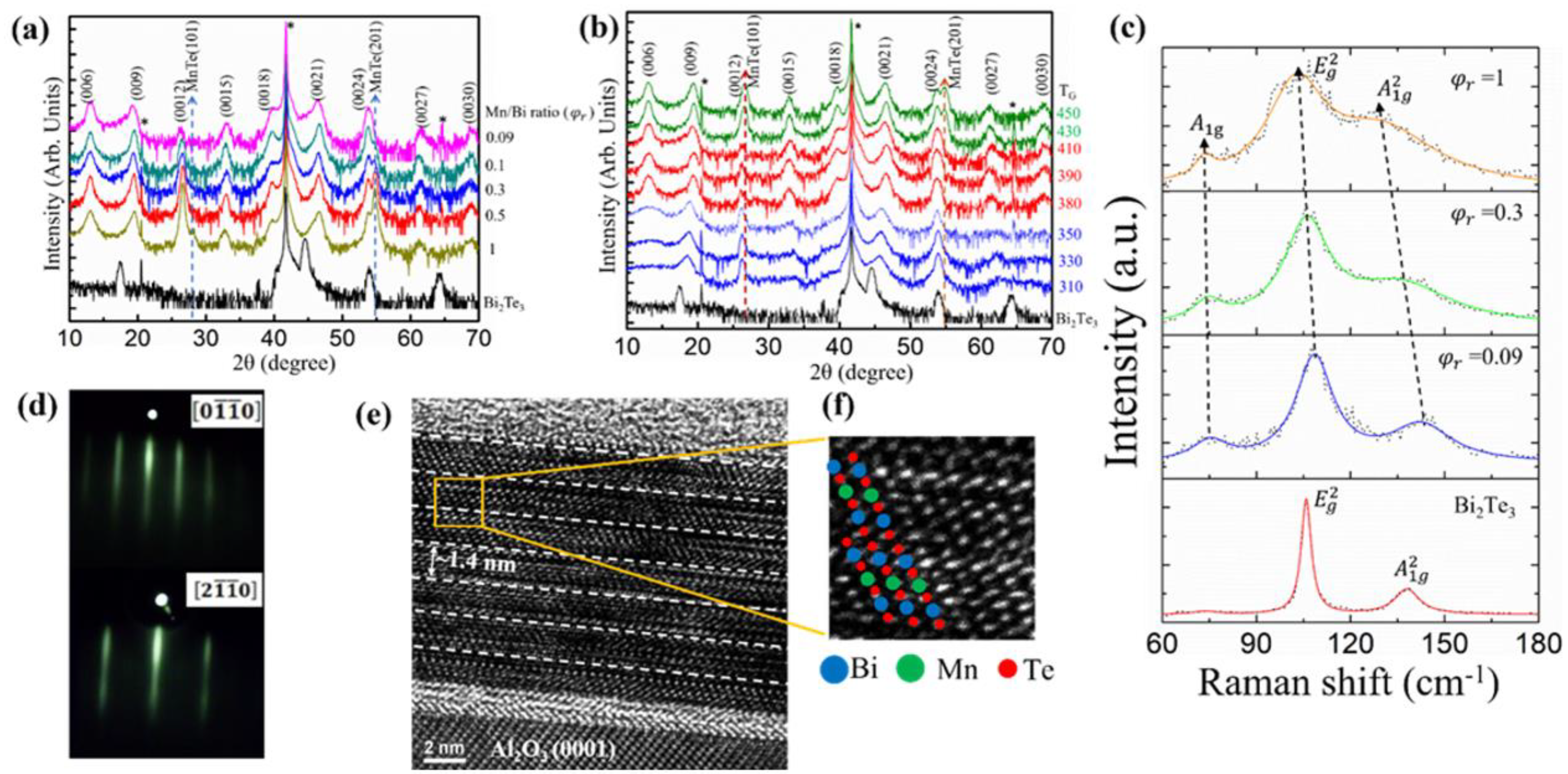
Abstract
:1. Introduction
2. Experimental Section
3. Results and Discussion
3.1. Structural Characterizations
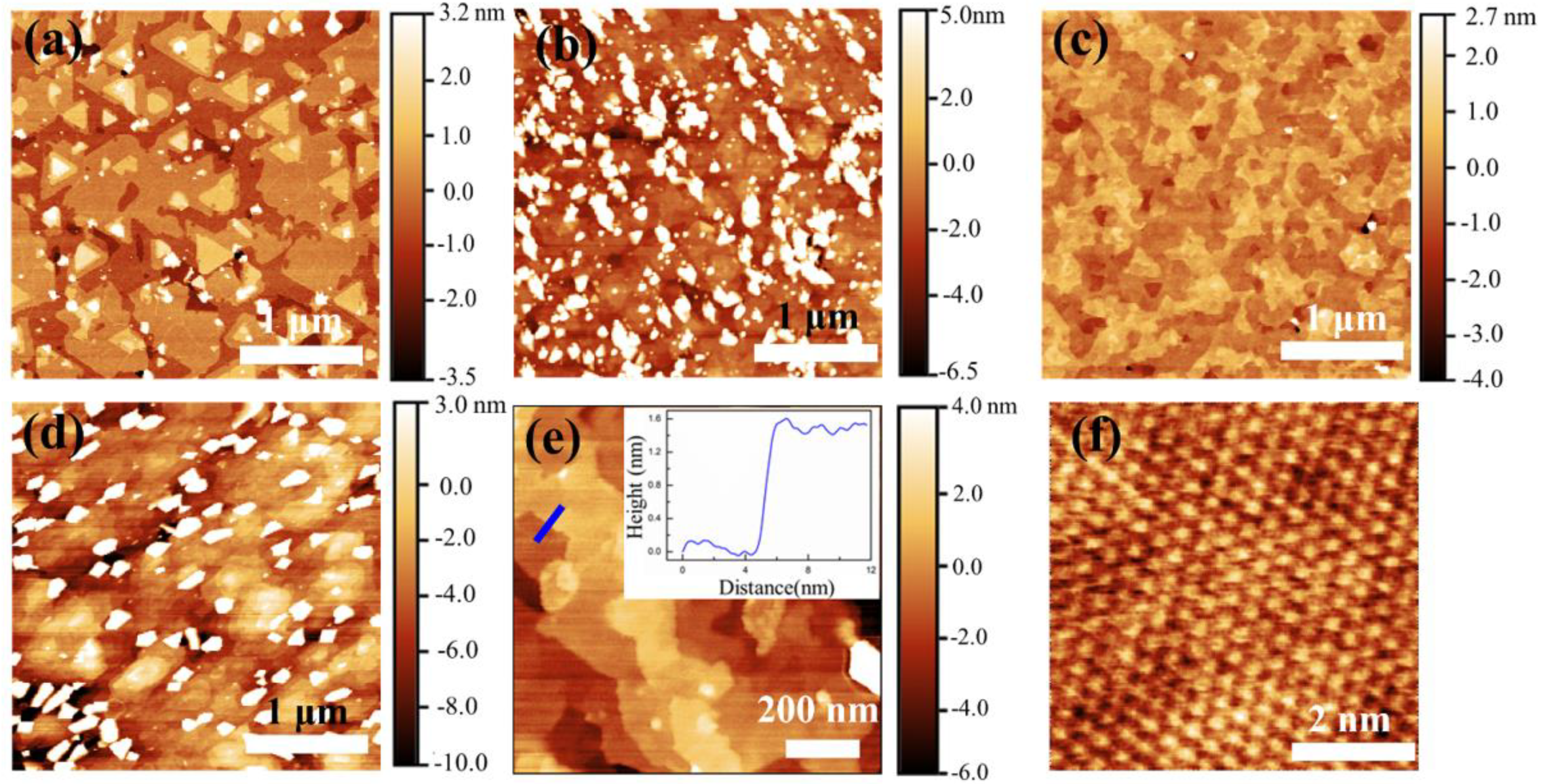
3.2. Surface Morphology
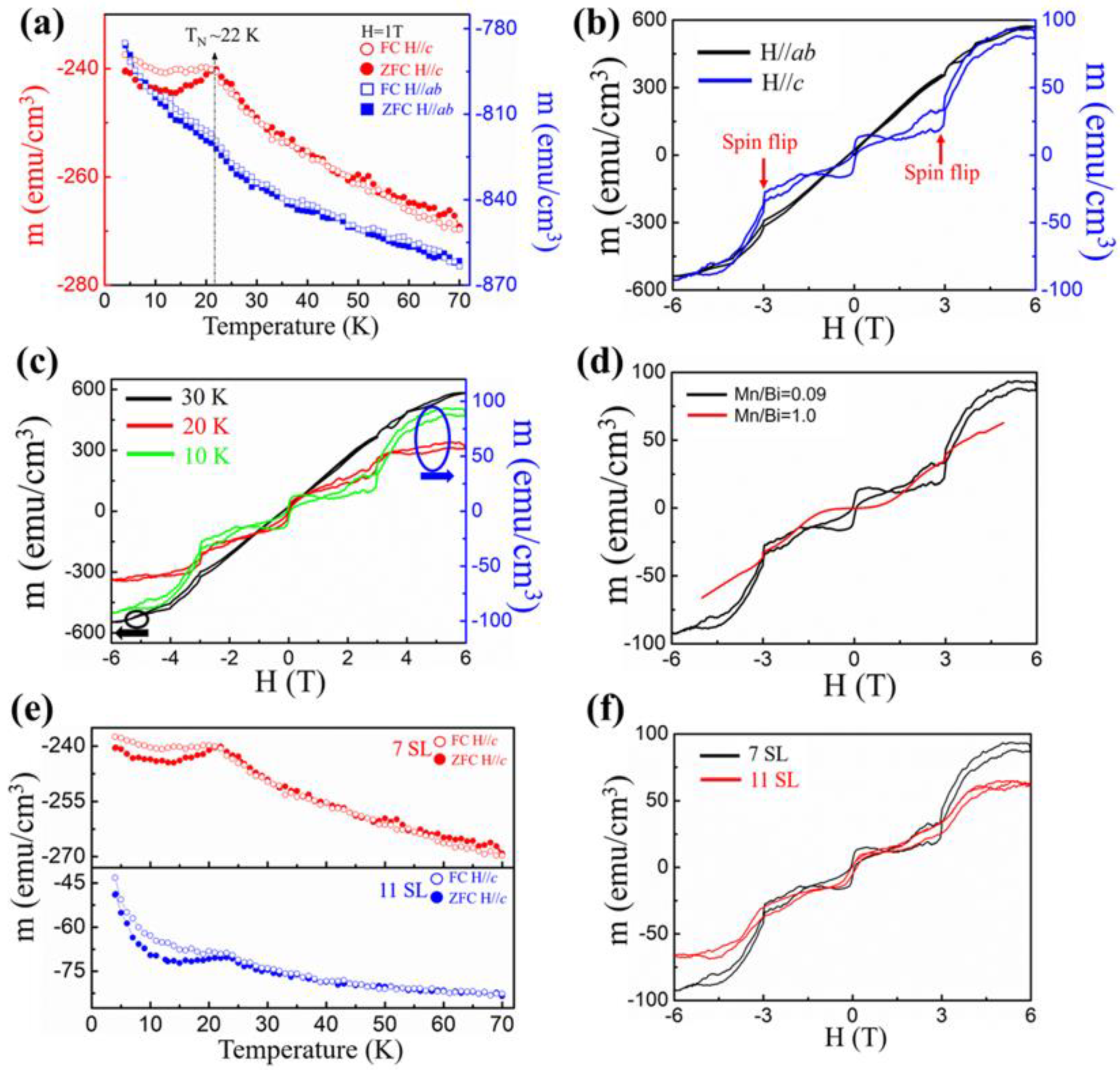
3.3. Magnetic Properties
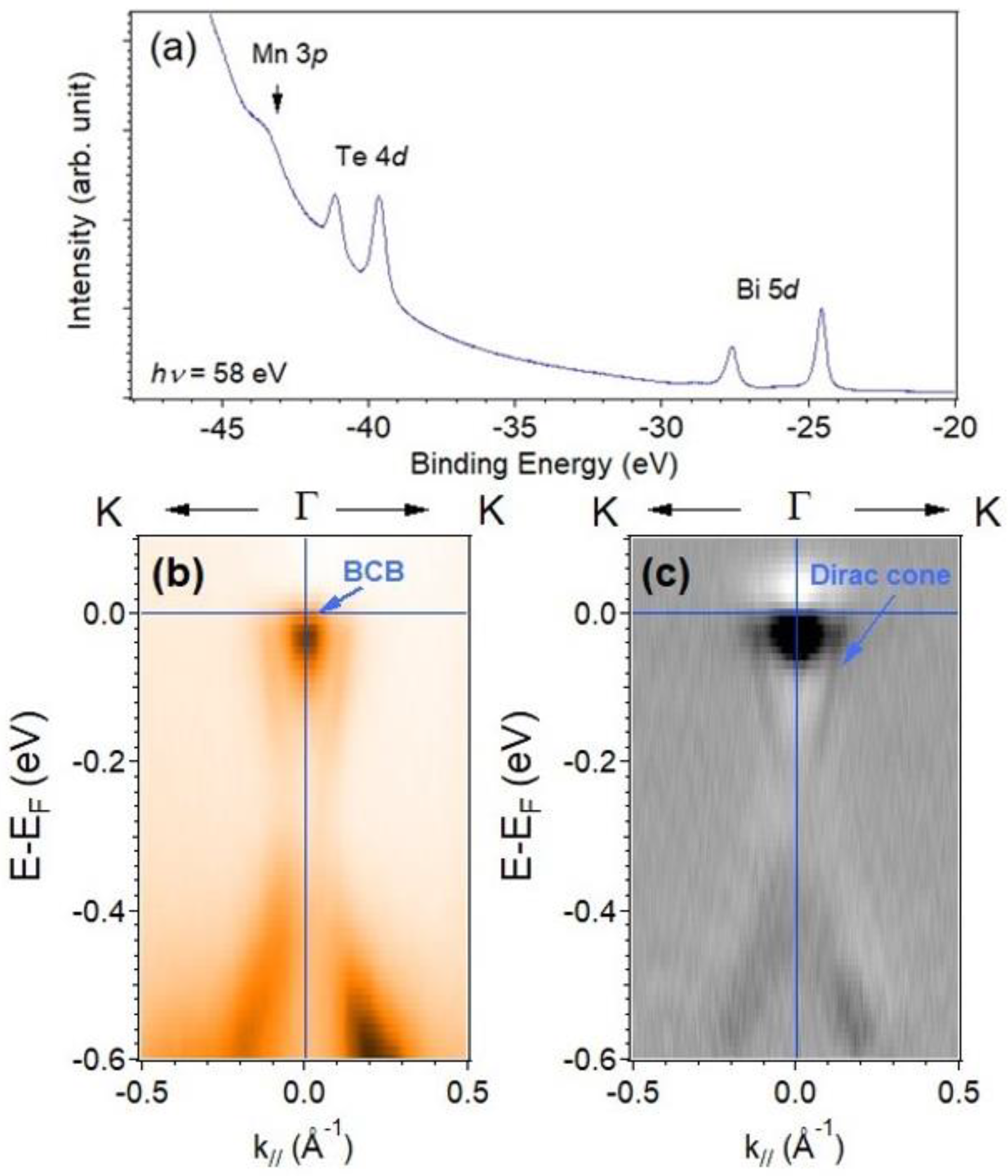
3.4. Band Structure
4. Conclusions
Supplementary Materials
Author Contributions
Funding
Data Availability Statement
Acknowledgments
Conflicts of Interest
References
- Tokura, Y.; Yasuda, K.; Tsukazaki, A. Magnetic topological insulators. Nat. Rev. Phys. 2019, 1, 126–143. [Google Scholar] [CrossRef]
- Yu, R.; Zhang, W.; Zhang, H.-J.; Zhang, S.-C.; Dai, X.; Fang, Z. Quantized Anomalous Hall Effect in Magnetic Topological Insulators. Science 2010, 329, 61–64. [Google Scholar] [CrossRef] [Green Version]
- Chang, C.Z.; Zhang, J.S.; Feng, X.; Shen, J.; Zhang, Z.C.; Guo, M.H.; Li, K.; Ou, Y.B.; Wei, P.; Wang, L.L.; et al. Experimental Observation of the Quantum Anomalous Hall Effect in a Magnetic Topological Insulator. Science 2013, 340, 167–170. [Google Scholar] [CrossRef] [PubMed] [Green Version]
- Chang, C.Z.; Zhao, W.W.; Kim, D.Y.; Zhang, H.J.; Assaf, B.A.; Heiman, D.; Zhang, S.C.; Liu, C.X.; Chan, M.H.W.; Moodera, J.S. High-precision realization of robust quantum anomalous Hall state in a hard ferromagnetic topological insulator. Nat. Mater. 2015, 14, 473–477. [Google Scholar] [CrossRef] [Green Version]
- Checkelsky, J.G.; Yoshimi, R.; Tsukazaki, A.; Takahashi, K.S.; Kozuka, Y.; Falson, J.; Kawasaki, M.; Tokura, Y. Trajectory of the anomalous Hall effect towards the quantized state in a ferromagnetic topological insulator. Nat. Phys. 2014, 10, 731. [Google Scholar] [CrossRef] [Green Version]
- Mogi, M.; Kawamura, M.; Yoshimi, R.; Tsukazaki, A.; Kozuka, Y.; Shirakawa, N.; Takahashi, K.S.; Kawasaki, M.; Tokura, Y. A magnetic heterostructure of topological insulators as a candidate for an axion insulator. Nat. Mater. 2017, 16, 516–522. [Google Scholar] [CrossRef] [PubMed]
- Xiao, D.; Jiang, J.; Shin, J.H.; Wang, W.B.; Wang, F.; Zhao, Y.F.; Liu, C.X.; Wu, W.D.; Chan, M.H.W.; Samarth, N.; et al. Realization of the Axion Insulator State in Quantum Anomalous Hall Sandwich Heterostructures. Phys. Rev. Lett. 2018, 120, 056801. [Google Scholar] [CrossRef] [Green Version]
- Mogi, M.; Kawamura, M.; Tsukazaki, A.; Yoshimi, R.; Takahashi, K.S.; Kawasaki, M.; Tokura, Y. Tailoring tricolor structure of magnetic topological insulator for robust axion insulator. Sci. Adv. 2017, 3, eaao1669. [Google Scholar] [CrossRef] [PubMed] [Green Version]
- Grauer, S.; Fijalkowski, K.; Schreyeck, S.; Winnerlein, M.; Brunner, K.; Thomale, R.; Gould, C.; Molenkamp, L. Scaling of the Quantum Anomalous Hall Effect as an Indicator of Axion Electrodynamics. Phys. Rev. Lett. 2017, 118, 246801. [Google Scholar] [CrossRef] [PubMed] [Green Version]
- Allen, M.; Cui, Y.; Ma, E.Y.; Mogi, M.; Kawamura, M.; Cosma Fulga, I.; Goldhaber-Gordon, D.; Tokura, Y.; Shen, Z.-X. Visualization of an axion insulating state at the transition between 2 chiral quantum anomalous Hall states. Proc. Natl. Acad. Sci. USA 2019, 116, 14511–14515. [Google Scholar] [CrossRef] [Green Version]
- Otrokov, M.M.; Klimovskikh, I.I.; Bentmann, H.; Estyunin, D.; Zeugner, A.; Aliev, Z.S.; Gass, S.; Wolter, A.U.B.; Koroleva, A.V.; Shikin, A.M.; et al. Prediction and observation of an antiferromagnetic topological insulator. Nature 2019, 576, 416–422. [Google Scholar] [CrossRef] [PubMed]
- Liu, C.; Wang, Y.; Li, H.; Wu, Y.; Li, Y.; Li, J.; He, K.; Xu, Y.; Zhang, J.; Wang, Y.; et al. Robust axion insulator and Chern insulator phases in a two-dimensional antiferromagnetic topological insulator. Nat. Mater. 2020, 19, 522–527. [Google Scholar] [CrossRef] [PubMed] [Green Version]
- Li, J.; Li, Y.; Du, S.; Wang, S.; Gu, B.-L.; Zhang, S.-C.; He, K.; Duan, W.; Xu, Y. Intrinsic magnetic topological insulators in van der Waals layered MnBi2Te4 family materials. Sci. Adv. 2019, 5, eaaw5685. [Google Scholar] [CrossRef] [PubMed] [Green Version]
- Liu, C.; Wang, Y.; Yang, M.; Mao, J.; Li, H.; Li, Y.; Li, J.; Zhu, H.; Wang, J.; Li, L.; et al. Magnetic-field-induced robust zero Hall plateau state in MnBi2Te4 Chern insulator. Nat. Comm. 2021, 12, 4647. [Google Scholar] [CrossRef] [PubMed]
- Zeugner, A.; Nietschke, F.; Wolter, A.U.B.; Gaß, S.; Vidal, R.C.; Peixoto, T.R.F.; Pohl, D.; Damm, C.; Lubk, A.; Hentrich, R.; et al. Chemical Aspects of the Candidate Antiferromagnetic Topological Insulator MnBi2Te4. Chem. Mater. 2019, 31, 2795–2806. [Google Scholar] [CrossRef] [Green Version]
- Chen, Y.J.; Xu, L.X.; Li, J.H.; Li, Y.W.; Wang, H.Y.; Zhang, C.F.; Li, H.; Wu, Y.; Liang, A.J.; Chen, C.; et al. Topological Electronic Structure and Its Temperature Evolution in Antiferromagnetic Topological Insulator MnBi2Te4. Phys. Rev. X 2019, 9, 041040. [Google Scholar] [CrossRef] [Green Version]
- Deng, Y.; Yu, Y.; Shi, M.Z.; Guo, Z.; Xu, Z.; Wang, J.; Chen, X.H.; Zhang, Y. Quantum anomalous Hall effect in intrinsic magnetic topological insulator MnBi2Te4. Science 2020, 367, 895–900. [Google Scholar] [CrossRef] [Green Version]
- Hao, Y.J.; Liu, P.F.; Feng, Y.; Ma, X.M.; Schwier, E.F.; Arita, M.; Kumar, S.; Hu, C.W.; Lu, R.E.; Zeng, M. Gapless Surface Dirac Cone in Antiferromagnetic Topological Insulator MnBi2Te4. Phys. Rev. X 2019, 9, 041038. [Google Scholar] [CrossRef] [Green Version]
- He, K. MnBi2Te4-family intrinsic magnetic topological materials. npj Quant. Mater. 2020, 5, 90. [Google Scholar] [CrossRef]
- Zhao, Y.; Liu, Q. Routes to realize the axion-insulator phase in MnBi2Te4(Bi2Te3)n family. Appl. Phys. Lett. 2021, 119, 060502. [Google Scholar] [CrossRef]
- Ovchinnikov, D.; Huang, X.; Lin, Z.; Fei, Z.; Cai, J.; Song, T.; He, M.; Jiang, Q.; Wang, C.; Li, H. Intertwined Topological and Magnetic Orders in Atomically Thin Chern Insulator MnBi2Te4. Nano Lett. 2021, 21, 2544–2550. [Google Scholar] [CrossRef] [PubMed]
- Zhang, S.; Wang, R.; Wang, X.P.; Wei, B.Y.; Chen, B.B.; Wang, H.Q.; Shi, G.; Wang, F.; Jia, B.; Ouyang, Y.P.; et al. Experimental observation of the gate-controlled reversal of the anomalous Hall effect in the intrinsic magnetic topological insulator MnBi2Te4 device. Nano Lett. 2020, 20, 709–714. [Google Scholar] [CrossRef] [PubMed] [Green Version]
- Zhang, D.Q.; Shi, M.J.; Zhu, T.S.; Xing, D.Y.; Zhang, H.J.; Wang, J. Topological Axion States in the Magnetic Insulator MnBi2Te4 with the Quantized Magnetoelectric Effect. Phys. Rev. Lett. 2019, 122, 206401. [Google Scholar] [CrossRef] [PubMed] [Green Version]
- Du, M.-H.; Yan, J.; Cooper, V.R.; Eisenbach, M. Tuning Fermi Levels in Intrinsic Antiferromagnetic Topological Insulators MnBi2Te4 and MnBi4Te7 by Defect Engineering and Chemical Doping. Adv. Funct. Mater. 2021, 31, 2006516. [Google Scholar] [CrossRef]
- Hou, F.; Yao, Q.; Zhou, C.-S.; Ma, X.-M.; Han, M.; Hao, Y.-J.; Wu, X.; Zhang, Y.; Sun, H.; Liu, C.; et al. Te-Vacancy-Induced Surface Collapse and Reconstruction in Antiferromagnetic Topological Insulator MnBi2Te4. ACS Nano 2020, 14, 11262–11272. [Google Scholar] [CrossRef] [PubMed]
- He, L.; Kou, X.; Wang, K.L. Review of 3D topological insulator thin-film growth by molecular beam epitaxy and potential applications. Phys. Status Solidi RRL 2013, 7, 50–63. [Google Scholar] [CrossRef]
- Chen, X.; Ma, X.C.; He, K.; Jia, J.-F.; Xue, Q.K. Molecular Beam Epitaxial Growth of Topological Insulators. Adv. Mater. 2011, 23, 1162–1165. [Google Scholar] [CrossRef] [PubMed]
- Zhu, W.; Song, C.; Liao, L.; Zhou, Z.; Bai, H.; Zhou, Y.; Pan, F. Quantum anomalous Hall insulator state in ferromagnetically ordered MnBi2Te4/VBi2Te4 heterostructures. Phys. Rev. B 2020, 102, 085111. [Google Scholar] [CrossRef]
- Fu, H.; Liu, C.-X.; Yan, B. Exchange bias and quantum anomalous Hall effect in the MnBi2Te4/CrI3 heterostructure. Sci. Adv. 2020, 6, eaaz0948. [Google Scholar] [CrossRef] [Green Version]
- Li, Z.; Li, J.; He, K.; Wan, X.; Duan, W.; Xu, Y. Tunable interlayer magnetism and band topology in van der Waals heterostructures of MnBi2Te4-family materials. Phys. Rev. B 2020, 102, 081107. [Google Scholar] [CrossRef]
- Fukasawa, T.; Kusaka, S.; Sumida, K.; Hashizume, M.; Ichinokura, S.; Takeda, Y.; Ideta, S.; Tanaka, K.; Shimizu, R.; Hitosugi, T.; et al. Absence of ferromagnetism in MnBi2Te4/Bi2Te3 down to 6 K. Phys. Rev. B 2021, 103, 205405. [Google Scholar] [CrossRef]
- Rienks, E.D.L.; Wimmer, S.; Sanchez-Barriga, J.; Caha, O.; Mandal, P.S.; Ruzicka, J.; Ney, A.; Steiner, H.; Volobuev, V.V.; Groiss, H.; et al. Large magnetic gap at the Dirac point in Bi2Te3/MnBi2Te4 heterostructures. Nature 2019, 576, 423–428. [Google Scholar] [CrossRef] [PubMed] [Green Version]
- Zhu, K.J.; Bai, Y.H.; Hong, X.Y.; Geng, Z.H.; Jiang, Y.Y.; Liu, R.X.; Li, Y.Z.; Shi, M.; Wang, L.L.; Li, W.; et al. Investigating and manipulating the molecular beam epitaxy growth kinetics of intrinsic magnetic topological insulator MnBi2Te4 with in situ angle-resolved photoemission spectroscopy. J. Phys. Condens. Matter 2020, 32, 475002. [Google Scholar] [CrossRef] [PubMed]
- Lapano, J.; Nuckols, L.; Mazza, A.R.; Pai, Y.Y.; Zhang, J.; Lawrie, B.; Moore, R.G.; Eres, G.; Lee, H.N.; Du, M.H.; et al. Adsorption controlled growth of MnTe(Bi2Te3)n by molecular beam epitaxy exhibiting stoichiometry-controlled magnetism. Phys. Rev. Mater. 2020, 4, 111201. [Google Scholar] [CrossRef]
- Trang, C.X.; Li, Q.; Yin, Y.; Hwang, J.; Akhgar, G.; Bernardo, I.D.; Grubišić-Čabo, A.; Tadich, A.; Fuhrer, M.S.; Edmonds, M.T.; et al. Crossover from 2D Ferromagnetic Insulator to Wide Band Gap Quantum Anomalous Hall Insulator in Ultrathin MnBi2Te4. ACS Nano 2021, 15, 13444–13452. [Google Scholar] [CrossRef] [PubMed]
- Kagerer, P.; Fornari, C.I.; Buchberger, S.; Morelhao, S.L.; Vidal, R.C.; Tcakaev, A.; Zabolotnyy, V.; Weschke, E.; Hinkov, V.; Kamp, M.; et al. Molecular beam epitaxy of antiferromagnetic (MnBi2Te4)(Bi2Te3) thin films on BaF2 (111). J. Appl. Phys. 2020, 128, 135303. [Google Scholar] [CrossRef]
- Gong, Y.; Guo, J.W.; Li, J.H.; Zhu, K.J.; Liao, M.H.; Liu, X.Z.; Zhang, Q.H.; Gu, L.; Tang, L.; Feng, X.; et al. Experimental Realization of an Intrinsic Magnetic Topological Insulator. Chin. Phys. Lett. 2019, 36, 076801. [Google Scholar] [CrossRef] [Green Version]
- Zhao, Y.-F.; Zhou, L.-J.; Wang, F.; Wang, G.; Song, T.; Ovchinnikov, D.; Yi, H.; Mei, R.; Wang, K.; Chan, M.H.W.; et al. Even-Odd Layer-Dependent Anomalous Hall Effect in Topological Magnet MnBi2Te4 Thin Films. Nano Lett. 2021, 21, 7691–7698. [Google Scholar] [CrossRef] [PubMed]
- Tung, Y.; Chong, C.W.; Liao, C.W.; Chang, C.H.; Huang, S.Y.; Chuang, P.-Y.; Lee, M.K.; Cheng, C.-M.; Li, Y.C.; Liu, C.P.; et al. Tuning the transport and magnetism in a Cr-Bi2Se3 topological insulator by Sb doping. RSC Adv. 2017, 7, 47789–47795. [Google Scholar] [CrossRef] [Green Version]
- Su, S.H.; Chuang, P.-Y.; Lee, J.-C.; Chong, C.-W.; Li, Y.W.; Lin, Z.M.; Chen, Y.-C.; Cheng, C.-M.; Huang, J.C.A. Spin-to-Charge Conversion Manipulated by Fine-Tuning the Fermi Level of Topological Insulator (Bi1–xSbx)2Te3. ACS Appl. Electron. Mater. 2021, 3, 2988–2994. [Google Scholar] [CrossRef]
- Su, S.H.; Chuang, P.-Y.; Chen, H.Y.; Wang, C.-H.; Chen, W.-C.; Tsuei, K.-D.; Lee, C.-K.; Yu, S.-H.; Chou, M.M.-C.; Tu, L.-W.; et al. Topological Proximity-Induced Dirac Fermion in Two-Dimensional Antimonene. ACS Nano 2021, 15, 15085–15095. [Google Scholar] [CrossRef]
- Li, H.; Liu, S.; Liu, C.; Zhang, J.; Xu, Y.; Yu, R.; Wu, Y.; Zhang, Y.; Fan, S. Antiferromagnetic topological insulator MnBi2Te4: Synthesis and magnetic properties. Phys. Chem. Chem. Phys. 2020, 22, 556–563. [Google Scholar] [CrossRef] [PubMed] [Green Version]
- Silva, A.S.; Guimaraes, E.V.; Cano, N.F.; Silva, R.S. Study of vibrational properties of Bi2-xMnxTe3 nanocrystals in host glass: Effect of xMn-concentration. J. Raman Spectrosc. 2021, 1–9. [Google Scholar] [CrossRef]
- Harrison, S.E.; Li, S.; Huo, Y.; Zhou, B.; Harris, J.S. Two-step growth of high quality Bi2Te3 thin films on Al2O3 (0001) by molecular beam epitaxy. Appl. Phys. Lett. 2013, 102, 171906. [Google Scholar] [CrossRef]
- Tung, Y.; Chiang, Y.F.; Chong, C.W.; Deng, Z.X.; Chen, Y.C.; Huang, J.C.A.; Cheng, C.-M.; Pi, T.-W.; Tsuei, K.-D.; Li, Z.; et al. Growth and characterization of molecular beam epitaxy-grown Bi2Te3−xSex topological insulator alloys. J. Appl. Phys. 2016, 119, 055303. [Google Scholar] [CrossRef]
- Liang, Z.; Luo, A.; Shi, M.; Zhang, Q.; Nie, S.; Ying, J.J.; He, J.-F.; Wu, T.; Wang, Z.; Xu, G.; et al. Mapping Dirac fermions in the intrinsic antiferromagnetic topological insulators (MnBi2Te4)(Bi2Te3)n (n = 0, 1). Phys. Rev. B 2020, 102, 161115. [Google Scholar] [CrossRef]
- Yan, J.Q.; Zhang, Q.; Heitmann, T.; Huang, Z.L.; Chen, K.Y.; Cheng, J.G.; Wu, W.D.; Vaknin, D.; Sales, B.C.; McQueeney, R.J. Crystal growth and magnetic structure of MnBi2Te4. Phys. Rev. Mater. 2019, 3, 064202. [Google Scholar] [CrossRef] [Green Version]
- Yang, S.; Xu, X.; Zhu, Y.; Niu, R.; Xu, C.; Peng, Y.; Cheng, X.; Jia, X.; Huang, Y.; Xu, X.; et al. Odd-Even Layer-Number Effect and Layer-Dependent Magnetic Phase Diagrams in MnBi2Te4. Phys. Rev. X 2021, 11, 011003. [Google Scholar] [CrossRef]
- Wu, J.Z.; Liu, F.C.; Sasase, M.; Ienaga, K.; Obata, Y.; Yukawa, R.; Horiba, K.; Kumigashira, H.; Okuma, S.; Inoshita, T.; et al. Natural van der Waals heterostructural single crystals with both magnetic and topological properties. Sci. Adv. 2019, 5, eaax9989. [Google Scholar] [CrossRef] [PubMed] [Green Version]
- Xie, H.; Wang, D.; Cai, Z.; Chen, B.; Guo, J.; Naveed, M.; Zhang, S.; Zhang, M.; Wang, X.; Fei, F.; et al. The mechanism exploration for zero-field ferromagnetism in intrinsic topological insulator MnBi2Te4 by Bi2Te3 intercalations. Appl. Phys. Lett. 2020, 116, 221902. [Google Scholar] [CrossRef]
- Kriegner, D.; Výborný, K.; Olejník, K.; Reichlová, H.; Novák, V.; Marti, X.; Gazquez, J.; Saidl, V.; Němec, P.; Volobuev, V.V. Multiple-stable anisotropic magnetoresistance memory in antiferromagnetic MnTe. Nat. Comm. 2016, 7, 11623. [Google Scholar] [CrossRef] [PubMed] [Green Version]
- Chuang, P.-Y.; Su, S.H.; Chong, C.-W.; Chen, Y.-F.; Chou, Y.-H.; Huang, J.C.A.; Chen, W.-C.; Cheng, C.-M.; Tsuei, K.-D.; Wang, C.-H.; et al. Anti-site defect effect on the electronic structure of a Bi2Te3 topological insulator. RSC Adv. 2018, 8, 423–428. [Google Scholar] [CrossRef] [Green Version]
- Hugdal, H.G.; Rex, S.; Nogueira, F.S.; Sudbø, A. Magnon-induced superconductivity in a topological insulator coupled to ferromagnetic and antiferromagnetic insulators. Phys. Rev. B 2018, 97, 195438. [Google Scholar] [CrossRef] [Green Version]


Publisher’s Note: MDPI stays neutral with regard to jurisdictional claims in published maps and institutional affiliations. |
© 2021 by the authors. Licensee MDPI, Basel, Switzerland. This article is an open access article distributed under the terms and conditions of the Creative Commons Attribution (CC BY) license (https://creativecommons.org/licenses/by/4.0/).
Share and Cite
Su, S.-H.; Chang, J.-T.; Chuang, P.-Y.; Tsai, M.-C.; Peng, Y.-W.; Lee, M.K.; Cheng, C.-M.; Huang, J.-C.A. Epitaxial Growth and Structural Characterizations of MnBi2Te4 Thin Films in Nanoscale. Nanomaterials 2021, 11, 3322. https://0-doi-org.brum.beds.ac.uk/10.3390/nano11123322
Su S-H, Chang J-T, Chuang P-Y, Tsai M-C, Peng Y-W, Lee MK, Cheng C-M, Huang J-CA. Epitaxial Growth and Structural Characterizations of MnBi2Te4 Thin Films in Nanoscale. Nanomaterials. 2021; 11(12):3322. https://0-doi-org.brum.beds.ac.uk/10.3390/nano11123322
Chicago/Turabian StyleSu, Shu-Hsuan, Jen-Te Chang, Pei-Yu Chuang, Ming-Chieh Tsai, Yu-Wei Peng, Min Kai Lee, Cheng-Maw Cheng, and Jung-Chung Andrew Huang. 2021. "Epitaxial Growth and Structural Characterizations of MnBi2Te4 Thin Films in Nanoscale" Nanomaterials 11, no. 12: 3322. https://0-doi-org.brum.beds.ac.uk/10.3390/nano11123322