1. Introduction
Transparent conductive oxide (TCO) films are important for various optoelectronic devices, such as transparent electrodes for light-emitting diodes and solar cells. Transparent thin films of indium tin oxide (ITO) and fluorine tin oxide (FTO) on glass substrates are the most widely used for these purposes [
1]. These common TCO thin films provide an electrical resistivity of 10
−3 Ω·cm and a high transmittance of over 80% in the visible-light region. However, these films absorb deep ultraviolet (DUV) and vacuum ultraviolet (VUV) light because of their bandgap energies. Therefore, a new type of transparent conductive film that is adaptable over a wide spectral range, spanning VUV to near-infrared (IR) light, would spur the development of novel optoelectronic devices. The refractive index of ITO films is approximately 1.9 in the visible-light region [
2], which reduces the transmittance of the electrode owing to reflections at the interface between the ITO and the glass substrate, for which the typical value is ~1.5. Thus, a transparent conductive film with a low refractive index is required.
Carbon nanotubes (CNTs) are conductive materials with excellent strength, electron conductivity, and flexibility [
3]. CNTs are generally used to fabricate composite materials comprising rubber, polymers, and so on [
4,
5]. The CNT networks in the composites are intertwined, and electrically conductive paths are formed by contact between CNTs [
6], where the conductivity depends on the diameter of the CNTs and the low resistance associated with the networks of CNTs with small diameters [
7]. Therefore, SWCNTs with small diameters are suitable for highly conductive films. CNT-inorganic composites afford exceptional optical, mechanical, electrical, and thermal properties [
8]. The CNT-SiO
2 composite is considered ideal due to its transparency over a wide wavelength range and the thermal stability of silica, which arises from the good chemical interaction between the CNTs and the silica matrix [
9,
10]. However, it is difficult to homogeneously disperse CNTs in a silica matrix because van der Waals forces cause the CNTs to aggregate [
10]. Additionally, the SWCNTs with excellent electronic properties tend to be damaged during the formation of the composite [
11]. The poor dispersibility in many precursor solutions and the lack of durability during composite fabrication are still serious challenges in producing SWCNT composites.
The formation methods of thin films can be classified into dry and wet processes. The dry processes, such as sputtering, ion beam deposition and so forth. is one of the methods to obtain high-quality thin films, and generally high cost due to necessary vacuum systems. On the other hand, the wet process is generally simple with no requirement of complicated facilities such as vacuum systems, and it is applicable to forming large-area thin films. The conventional TCO thin films with low resistivity are generally formed using the dry process. However, if the TCO thin film with low resistivity can be formed by using the wet process, it is a great advantage.
Our group developed a wet chemical process, the molecular precursor method (MPM), for fabricating thin films of various metals, metal oxides, and phosphate compounds [
12]. This method is based on the design of a metal complex and offers many advantages, such as excellent stability, homogeneity, miscibility, and coatability. Recently, we prepared an SiO
2 precursor solution that is highly miscible in an aqueous dispersion of MWCNTs and used UV irradiation at ambient temperature to fabricate a thin-film of a MWCNT/SiO
2 composite on a spin-coated precursor film [
13]. The electrical resistivity and transmittance of the mechanically robust composite thin film (8H pencil hardness), were 0.7 Ω·cm and >80% in both the visible and UV regions, respectively. These results suggest that MPM can produce a SWCNT-SiO
2 composite while preserving the excellent properties of the SWCNTs.
Herein, we report a promising composite thin film as a transparent and conductive material. The film has a thickness of 60 nm and an electrical resistivity of 10−3 Ω·cm. Except for the minimum transmittance of approximately 73% at approximately 273 nm in the DUV region, the film has a transparency exceeding 80% over a wide range, spanning 178 nm (VUV region) to the near IR region.
2. Materials and Methods
2.1. Materials
Tetraethyl orthosilicate (TEOS), oxalic acid, and 2-propanol were purchased from Kanto Chemical Co., Inc. (Tokyo, Japan), FUJI-FILM Wako Pure Chemical Corporation (Miyazaki, Japan), and Taisei Chemical Co., Ltd. (Tokyo, Japan). An ethanol dispersion of SWCNTs (0.2 mass%) (eDIPS-INK) was acquired from Meijo Nano Carbon Co., Ltd. (Aichi, Japan). Deionized water was purchased from Kyoei Pharmaceutical Co., Ltd. (Chiba, Japan). Ethanol (EtOH) was purchased from Ueno Chemical Industries, Ltd. (Tokyo, Japan) and dried on 4A molecular sieves prior to use. The other materials were used as received, without further purification. Polished quartz glass plates (20 × 20 × 1.5 mm3), Akishima Glass Co., Ltd., Tokyo, Japan) were ultrasonically cleaned with 2-propanol to remove organic molecules from the surfaces, thoroughly rinsed with deionized water, and oven-dried at 70 °C.
2.2. Preparation of SWCNT/SiO2 Composite Precursor Solution
An SiO
2 precursor solution (
SSilica) was prepared according to our previous study [
13]. A mixed solution of TEOS (1.3 g) and oxalic acid (1.1 g) dissolved in ethanol (10 g) was refluxed for 1 h (Si
4+ concentration of 0.5 mmol g
−1).
Ethanol was added to dilute a solution (SCNT) of the ethanol dispersion of SWCNTs (eDIPS-INK) to adjust the concentration to 0.1 mass%. SSilica and SCNT at room temperature were mixed to prepare seven different precursor solutions (C/Si molar ratios of 0.05–0.5) for fabricating the composite thin film. Each mixed solution was mechanically stirred for 1 h. The obtained solutions are denoted as Sx, where “x” indicates an alphabetical order from “a” to “g” that corresponds to the C/Si molar ratios of 0.05, 0.1, 0.15, 0.2, 0.3, 0.4, 0.5, respectively (see Table 1).
2.3. Fabrication of SWCNT-SiO2 Composite Thin Films by UV-Light Irradiation, and Post-Annealing Treatment
Each Sx (300 μL) solution was dropped onto a quartz glass substrate and was subsequently spin-coated in double-step mode (1st: 500 rpm for 5 s and 2nd: 2000 rpm for 30 s). The precursor films (Px) were obtained after preheating the spin-coated films in a drying oven at 70 °C for 10 min. A germicidal lamp was used to irradiate each Px set with a UV light (4 mW cm−2 at 254 nm) for 64 h in a clean bench. A digital thermocouple and hygrometer were respectively used to monitor the surface temperature of Px and the relative humidity of the clean bench during UV irradiation. The UV-irradiated films on the quartz glass substrate are denoted as Fx, corresponding to the applied Sx in the spin-coating process. The obtained thin film Ff with a C/Si ratio of 0.4 was heat treated at 500 °C for 1 h in an electric furnace to yield Ff-HT.
Additionally, the abovementioned procedure was used to obtain a CNT thin film (FCNT), following spin coating of the SCNT and preheating. The heat-treated FCNT-HT film was also obtained following heat treatment of FCNT at 500 °C for 1 h in an identical furnace.
2.4. Electrical and Optical Characterization of Thin Films
A four-probe method employing two multimeters (VOAC7512, Iwatsu and Model 2010 Multimeter, Keithley, Cleveland, OH, USA) and a regulated DC power supply (Model PAB 32-1.2, Kikusui Electronics Corp., Kanagawa, Japan) were used to measure the electrical voltage of Fa–Fg at 25 °C. Four gold-plated tungsten probes (FELL type, K&S, Washington, DC, USA) were placed at intervals of 1 mm, and a load of 0.1 kg was applied.
A UV-3600 spectrophotometer (Shimadzu, Kyoto, Japan) in double-beam mode with air as a reference was used to measure the transmittance spectra of Ff and Ff-HT in the 220–2600 nm range. A far-ultraviolet monochromator in single-beam mode (based on KV-200, Bunkohkeiki Co., Ltd., Tokyo, Japan), which was purged with nitrogen gas, was used for measurement in the wavelength range of 130–300 nm; the purging gas was used as a reference.
A MARY-102 ellipsometer was used to measure the refractive indices of Ff and Ff-HT (Five Lab, Kanagawa, Japan) at a wavelength of 632.8 nm and an incident angle of 70.07°. The refractive index was measured at 14 points on the films, and SiO2 (refractive index of 1.52) was used as the reference.
A haze meter COH7700 (Nippon Denshoku Industries Co., Ltd., Tokyo, Japan) was used to measure the haze of Ff and Ff-HT. The haze was calculated as the average value from five points on the films, excluding the highest and lowest values.
2.5. Structural Characterization of Thin Films
A Raman microspectrometer (LaBRAM HR800, Horiba Ltd., Kyoto, Japan) with a charge-coupled device detector in back-scattering geometry was used to measure the Raman spectra of five films: Pf, Ff, Ff-HT, FCNT, and FCNT-HT. A Nd-YAG laser (532 nm) with a spot diameter of 1 µm was used as the excitation source at an intensity of 13 mW. The exposure time was changed to determine the optimum conditions for peak detection. The spectra of Pf, Ff, and Ff-HT in the range of 250–2100 cm−1 were obtained with an exposure time of 60 s. The spectra of FCNT and FCNT-HT were obtained with an exposure time of 30 s. The spectra of Pf, Ff, and Ff-HT in the range of 100–250 cm−1 were obtained with an exposure time of 360 s, while the spectra of FCNT and FCNT-HT in the identical range were obtained with an exposure time of 180 s.
A Raman peak of the Si substrate at 520.64 cm−1 was used for wavelength calibration. A nonlinear least-squares method, which involved a Lorentz function, was used to deconvolute the Raman peaks in the range of 1200–1700 cm−1. OriginPro2018b (OriginLab Corporation, Northampton, MA, USA) was used for calculations, and the peak fitting converged with a χ2 tolerance value of 1 × 10⁻⁹.
2.6. Surface Morphology, Film Thickness, and Pencil Hardness of Thin Films
Field-emission scanning electron microscopy (FE-SEM) with a JSM-6701F microscope (JEOL Ltd., Tokyo, Japan) at an accelerating voltage of 5 kV was used to determine the surface morphologies of Pf, Ff, and FCNT. The average thickness of the SWCNT bundles in Pf and Ff was calculated from five randomly selected bundles.
Atomic force microscopy (AFM) equipment (OLS4500, OLYMPUS, Tokyo, Japan) was used to obtain three-dimensional (3D) AFM images of Ff, Ff-HT, FCNT, and FCNT-HT by scanning a 2 × 2 μm2 area, and the surface roughness was estimated.
Scanning transmission electron microscopy (STEM) and energy dispersive spectroscopy (EDS) in JEM-2100F (JEOL Ltd., Tokyo, Japan) at an accelerating voltage of 200 kV were used to analyze the cross-sectional morphology and elemental distribution of Ff and Ff–HT. The film surface was covered with a carbon film before the center of the sample was cut with a focused ion beam (FIB).
A stylus profilometer (DEKTAK-3, Sloan, Santa Barbara, CA, USA) was used to measure the film thicknesses of Pf, Fx, and Ff-HT. A portion of each precursor film was removed during sample preparation, using ethanol to expose the substrate. The differences at each level between the substrate and the resultant film were measured at five positions for each sample. The film thickness was calculated as the average value, excluding the highest and lowest values. In the case of Pf, the measurement was performed two days after the film formed.
A pencil scratch test (the Japanese Industrial Standard (JIS) K5400) was used to evaluate the pencil hardness of Ff and Ff-HT. The test involved an MJ-PHT pencil hardness meter (Sato Shouji Inc., Kanagawa, Japan) with a 0.75 kg load. Pencils (UNI, Mitsubishi Pencil Co., Ltd., Tokyo, Japan) with various hardness values were standardized in the hardening order from 6B to 9H and were used to scratch the film.
3. Results and Discussion
Although an aqueous dispersion of MWCNTs was used in our previous study [
13], the precursor solutions (
Sx) for the SWCNT-silica composite thin film can be prepared by mixing the Si
4+ complex of oxalic acid in ethanol and an ethanolic dispersion of SWCNTs. The coatability of
Sx on the quartz glass substrate was excellent and was independent of the SWCNT concentration. The surface temperature of each precursor film during exposure to UV was 20–40 °C, and the humidity in the clean bench was 20–50%. The various properties of the composite film
Ff with a C/Si ratio of 0.4 are examined in detail in the following sections because this thin film exhibited the lowest electrical resistivity.
3.1. Electrical Resistivity of Thin Films and SWCNT Concentration in Precursor
Table 1 lists the electrical resistivities of the composite thin films,
Fa–
Fg (thickness: 60–120 nm,
Supplementary Materials Figure S1). The volume concentration of SWCNTs was calculated on the assumption that the SWCNTs and SiO
2 were close packed; therefore, respective densities of 1.3 and 2.2 g cm
−3 were used [
14,
15]. Generally, the electrical resistivity of the composite decreased drastically near the percolation threshold, resulting in electrical resistivity at 3.3 vol.%, and reached the lowest value at 12 vol.% (
Table 1 and
Supplementary Materials Figure S2). The electrical resistivity of
Ff on the order of 10
−3 Ω·cm is comparable to that of the ordinary ITO and FTO glass substrates. This low resistivity is associated with the formation of a conductive network unique to CNTs [
10,
16].
Contrastingly, the lowest resistivity of the SWCNT-silica film was 6.6 Ω·cm; this film was formed by the sol-gel method, in which the maximum CNT concentration was 4 mass% [
17]. This concentration corresponds to films
Fb and
Fc, which had a proportionally low resistivity. In the case of the present MPM, the resistivity of
Ff was reduced by as much as three orders of magnitude because the CNT concentration could be further increased. Importantly, the Si
4+ complex did not interfere with the dispersion of the SWCNTs at high concentrations.
3.2. Optical Properties of Ff and Ff-HT
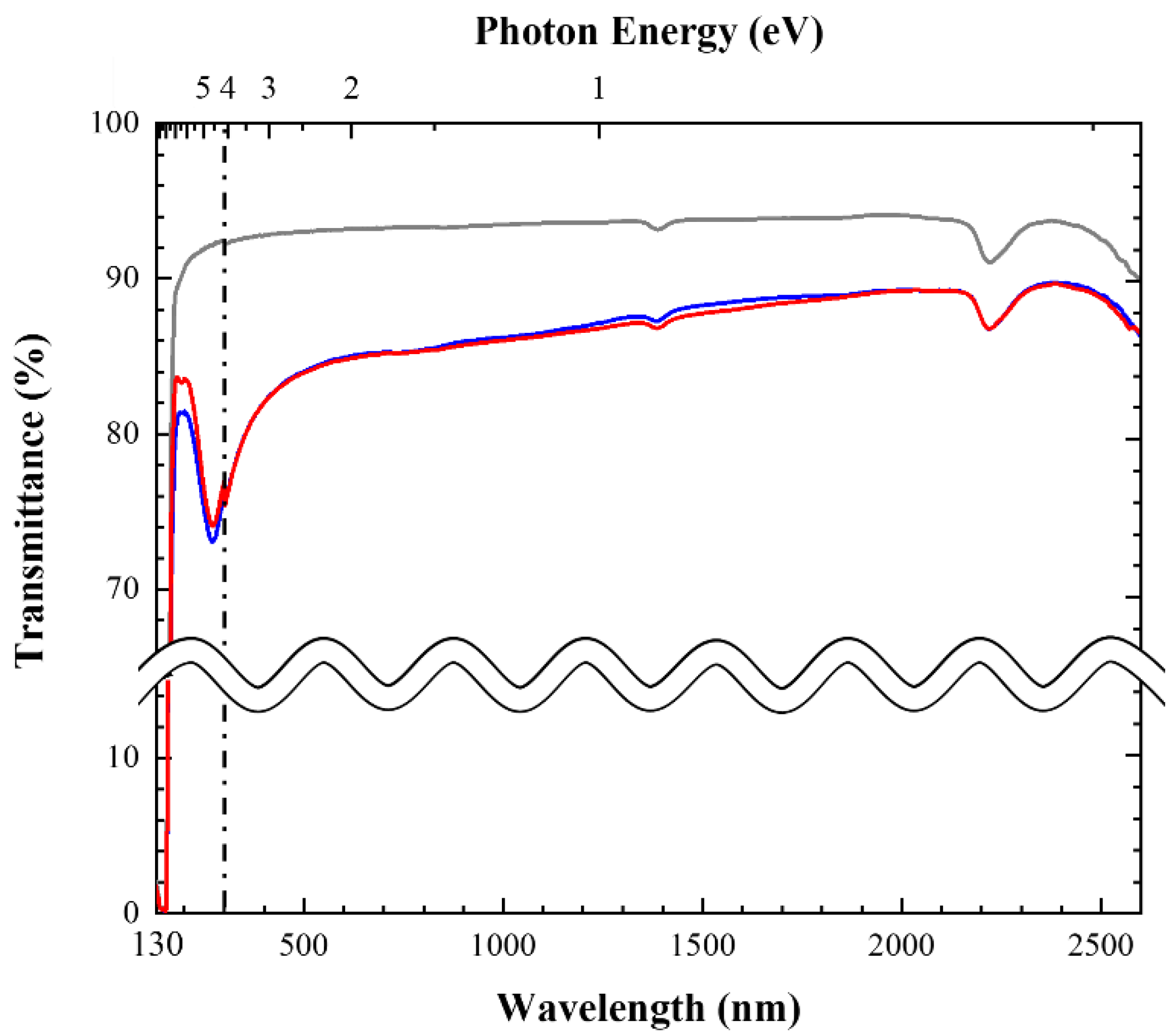
Figure 1 shows the transmittance spectra of
Ff,
Ff-HT, and the quartz glass substrate in the range of 130–2600 nm. The transmittance of
Ff was higher than 80% from 178 nm in the VUV region to the near IR region, and higher than 73% in the range of 220–352 nm. The corresponding value of
Ff-HT was 1–3% higher than that of
Ff. Because the quartz glass solely absorbed VUV light, it had the shortest wavelength absorption, and the transmittance consequently decreased because of the substrate thickness. The weak peak at 273 nm (4.5 eV) is due to the π-plasmon absorption of the CNTs, related to the polarization dependence and the optical properties of graphite [
18].
The refractive indices of Ff and Ff-HT were 1.49 and 1.48, respectively, and were comparable to 1.52 for SiO2. The haze values of Ff and Ff-HT were 1.5% and 1.0%, respectively, which indicate the flatness of the film surface (vide supra). Notably, current thin films with a low refractive index and haze are much more transparent than ordinary ITO and FTO.
3.3. Structural Characterization of Ff, Ff-HT, Pf, FCNT, and FCNT-HT
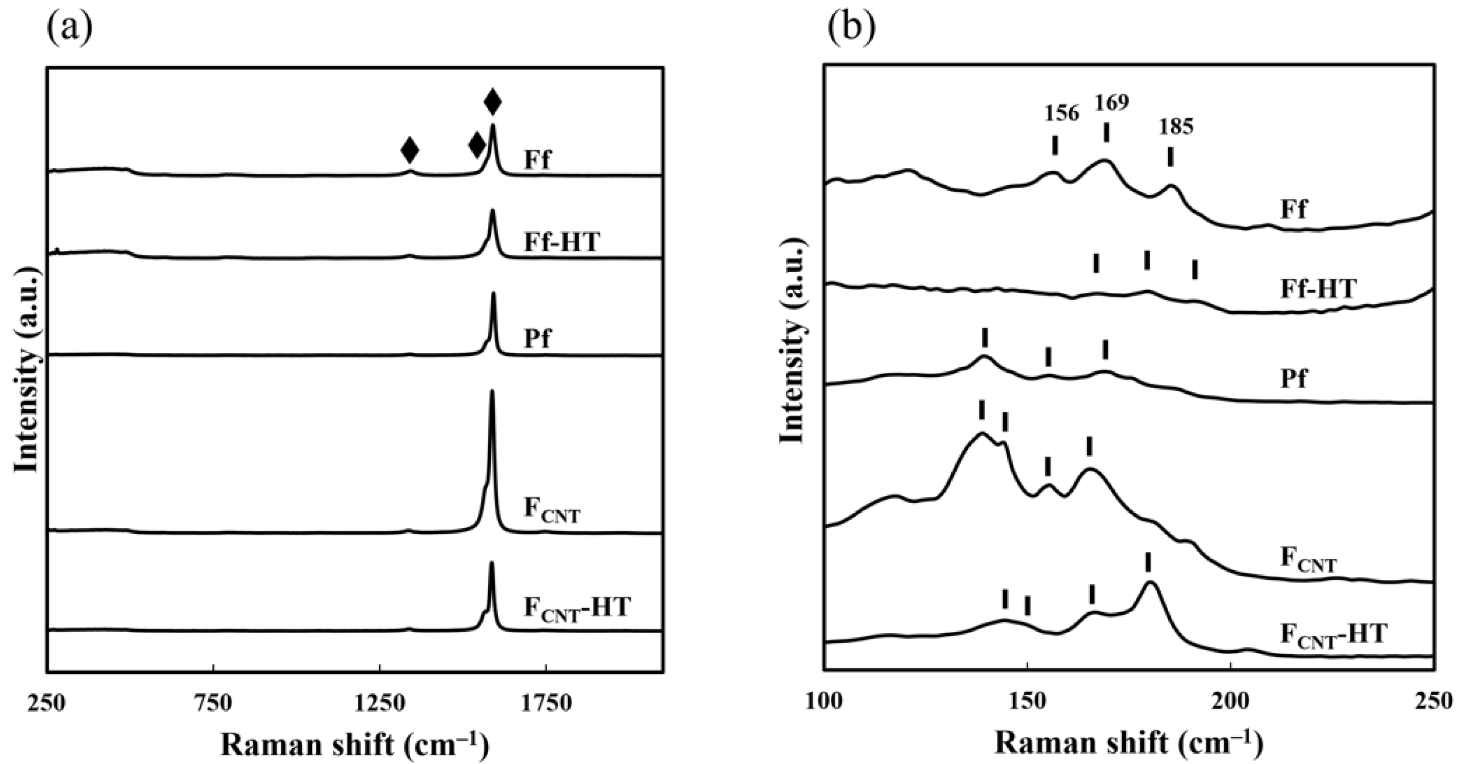
Figure 2 shows the Raman spectra of
Ff,
Ff-HT,
Pf,
FCNT, and
FCNT-HT. The three peaks at 1340, 1570, and 1590 cm
−1 in all films can be assigned to the D, G
−, and G
+ bands of CNT [
19,
20]. These three peaks were deconvoluted to evaluate the structural changes of the SWCNTs (
Supplementary Materials Figure S3).
The (G− + G+)/D ratios of FCNT and Pf were 52 and 42, respectively, suggesting that upon mixing the SWCNTs with the Si4+ complex of oxalic acid in ethanol, the number of defect sites in graphite preferentially increased. The (G− + G+)/D ratio for Ff is 7.1 and ~1/6 of that for Pf, indicating a significant increase in the number of defect sites upon UV irradiation. Thus, UV irradiation of Pf induced structural changes of the SWCNTs. Despite these significant structural changes, this method is still advantageous for forming highly conductive composites at room temperature.
The (G− + G+)/D ratios of FCNT-HT and Ff-HT were respectively 26 and 15, which are respectively half and twice the ratios before heat treatment. Therefore, the number of defect sites in the SWCNTs alone increased than for those embedded in the silica matrix, suggesting that the aforementioned increase in the number of defect sites after UV irradiation might be temporary and that the original graphite ones recovered after heat treatment. Notably, the SiO2 matrix plays an important role in preventing degradation of the graphite sites of the SWCNTs during heat treatment.
Multiple peaks in the range of 100–250 cm
−1, representing the radial breathing mode (RBM) of CNT [
20], were found: 139, 156, and 169 cm
−1 for
Pf; 156, 169, and 185 cm
−1 for
Ff; 167, 179, and 191 cm
−1 for
Ff-HT; 139, 144, 156, and 165 cm
−1 for
FCNT; 146, 152, 167, and 180 cm
−1 for
FCNT-HT. In comparison with the RBM peaks of
FCNT, those of
Ff shifted to higher energy, suggesting that dispersion of SiO
2 in the matrix led to the relaxation of the CNT bundles [
21].
3.4. Changes in the Film Thickness and Hardness for Pf after UV Irradiation and for Ff after Heat Treatment
The film thicknesses of
Pf,
Ff, and
Ff-HT were 110, 60, and 70 nm, respectively. Because the as-coated precursor film was too soft, the thickness measurement for
Pf was performed after keeping the film in the dark for 48 h at 25 °C; nevertheless, the pencil hardness of
Pf was less than 6B. Comparatively, the pencil hardness of
Ff and
Ff-HT was 4H and 9H, respectively. Therefore, UV irradiation of
Pf at room temperature and heat treatment of
Ff were both useful for forming robust composite thin films due to the stepwise removal of organic residues in the original precursor film and the UV-irradiated composite thin film, respectively. The film thickness of
Ff-HT may increase when oxygen atoms are embedded into the Si-O dangling bonds, as observed for an MWCNT composite that we previously prepared [
13].
3.5. Morphology of Surface and Cross-Section of Thin Films
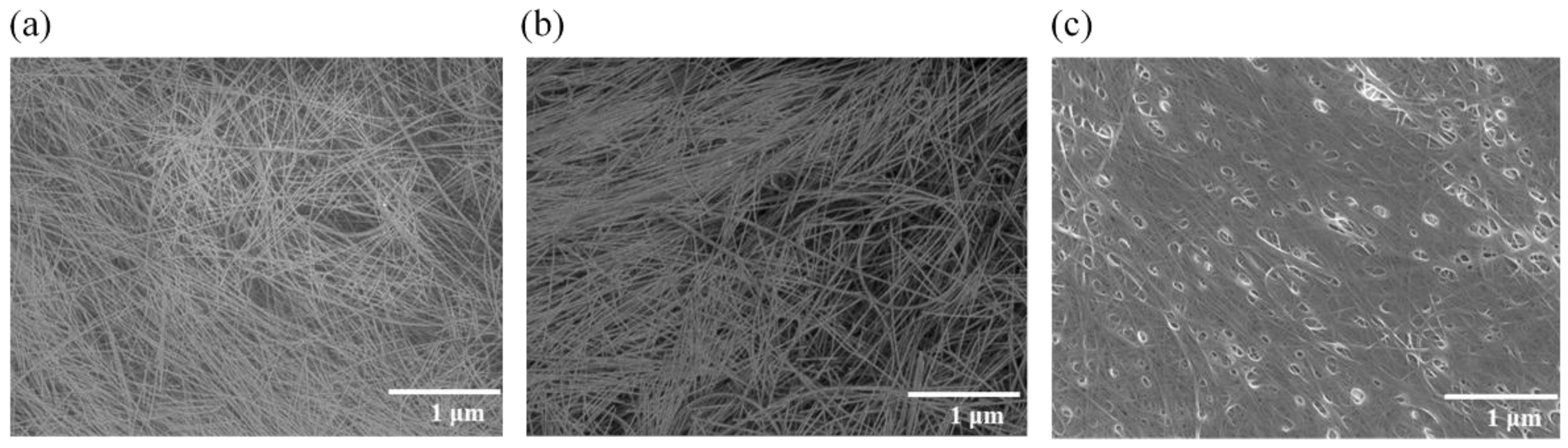
Figure 3 shows the FE-SEM images of
Ff,
Pf, and
FCNT. The SWCNT bundles in
Ff and
Pf (
Figure 3a,b) are randomly arrayed and the intertwined networks of SWCNT bundles have average diameters of ~16 nm. Comparatively,
FCNT, which was solidified with its dispersant, has many pinholes on its surface (
Figure 3c).
One bundle contains up to 250 molecules, assuming that one SWCNT molecule is 1 nm in diameter and that adjacent molecules connect directly to form a bundle with a diameter of 16 nm. These bundles with high aspect ratios are arranged horizontally toward the surface and are intertwined. Therefore, it is acceptable that the SWCNT molecules that were dispersed in finer units cannot be observed with FE-SEM. As the Si
4+ complex photodegraded, the molecular precursor enhanced the contact between the SWCNTs during film formation, resulting in densification of the SiO
2 matrix and a low electrical resistivity. In fact, the film thickness of
Ff decreased to almost half that of the precursor film,
Pf. Comparing the distribution of the SWCNT bundles in
Ff and
Pf, it is assumed that densification of the matrix occurred during UV irradiation without aggregation of the SWCNT bundles. From the 3D-AFM images, the surface roughness of
Ff and
Ff-HT was 3 nm, which was smaller than 7 and 9 nm for
FCNT and
FCNT-HT, respectively (
Supplementary Materials Figure S4).
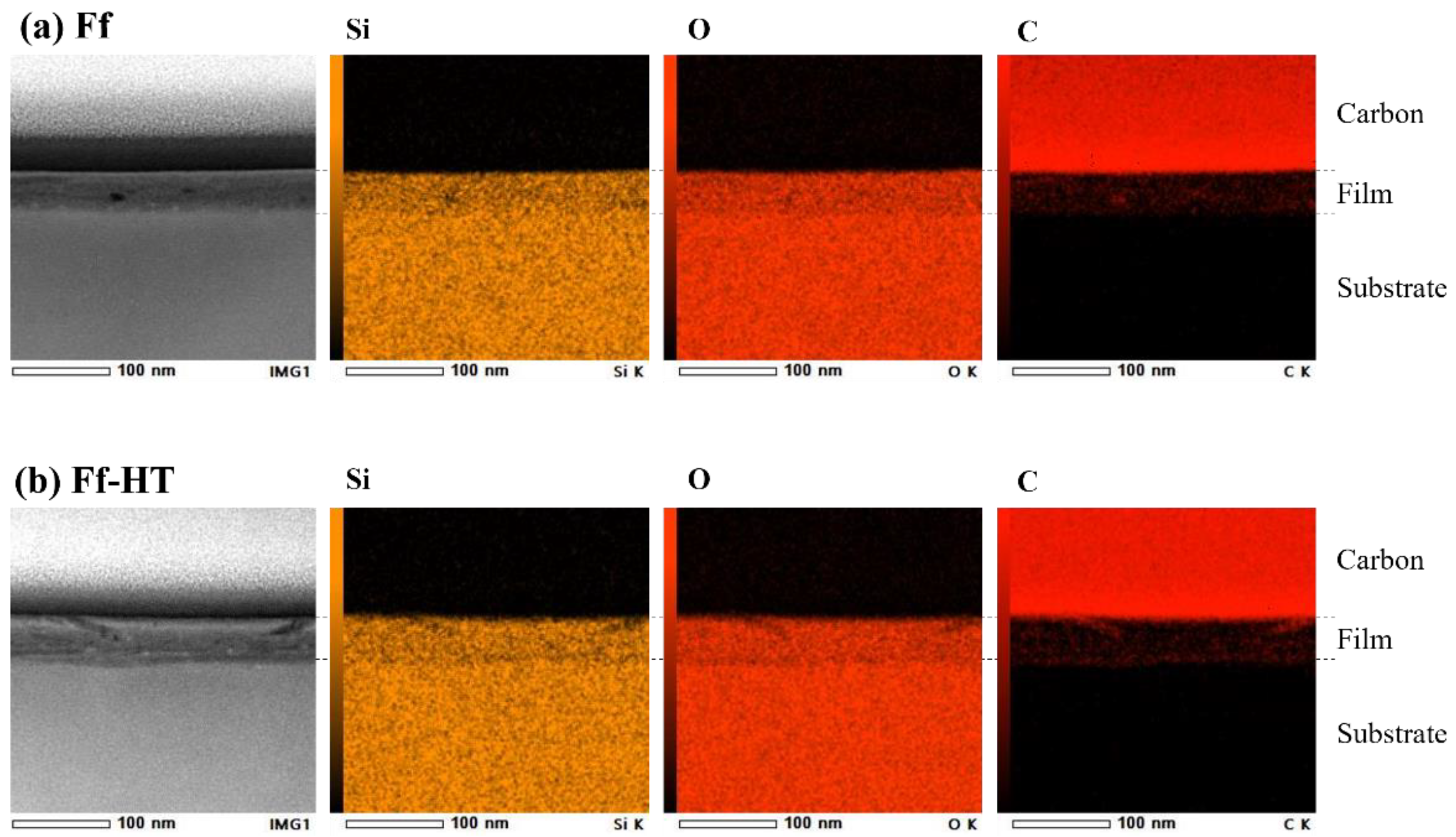
Figure 4 shows the cross-sectional STEM images and corresponding EDS elemental maps of
Ff and
Ff-HT. The interface and surfaces were smooth in both cases; there were no cracks or pinholes in the entire film. Importantly, there was little aggregation of the SWCNTs, resulting sufficient dispersion of the carbon atoms.


 ,
, 


