
Effect of Nano Copper on the Densification of Spark Plasma Sintered W–Cu Composites


 , ,
, , 
Abstract
:
1. Introduction
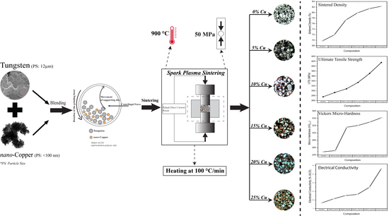
2. Experimental
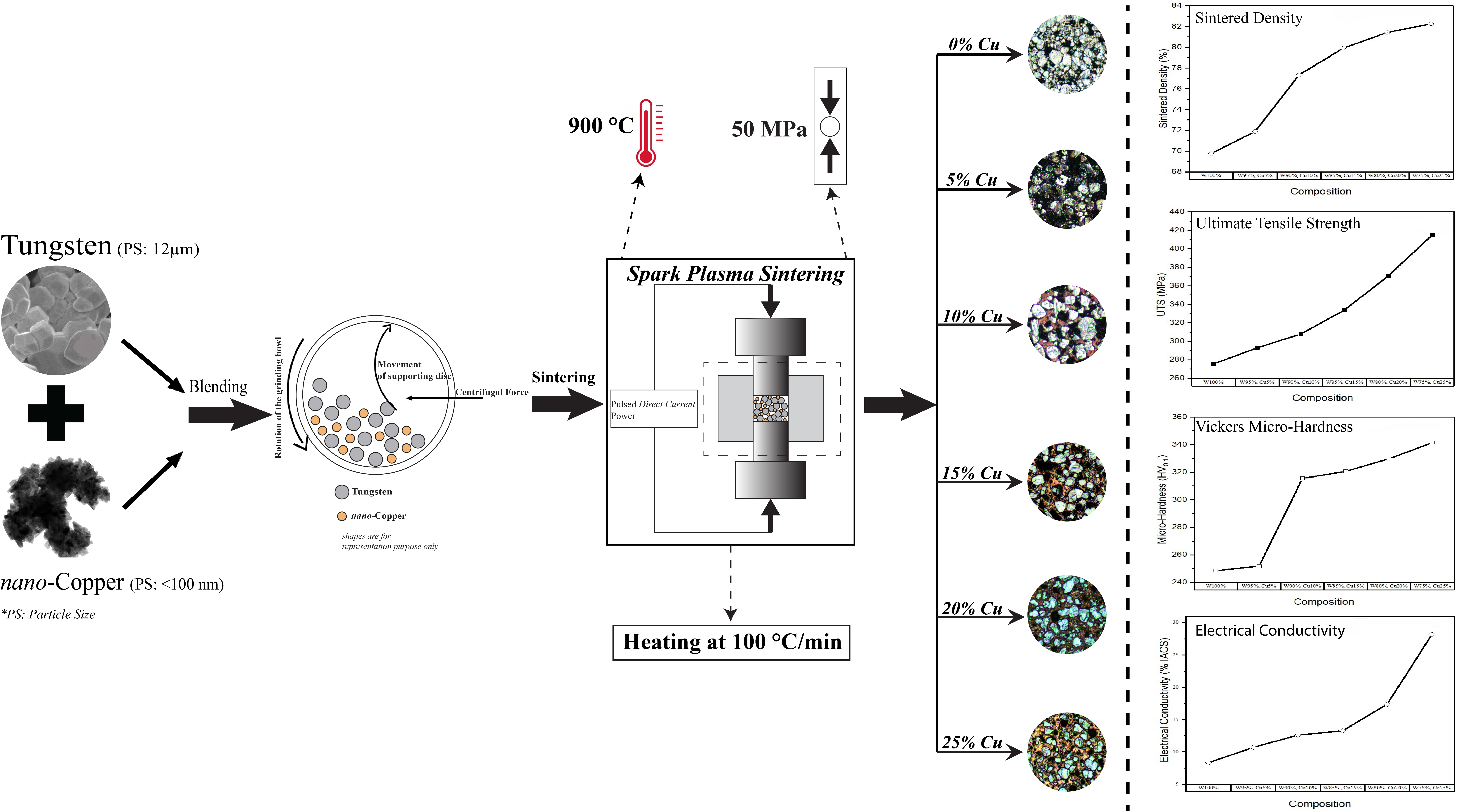
2.1. Materials
2.2. Spark Plasma Sintering (SPS)
2.3. Characterization of Sintered Samples
3. Results and Discussion
3.1. Density
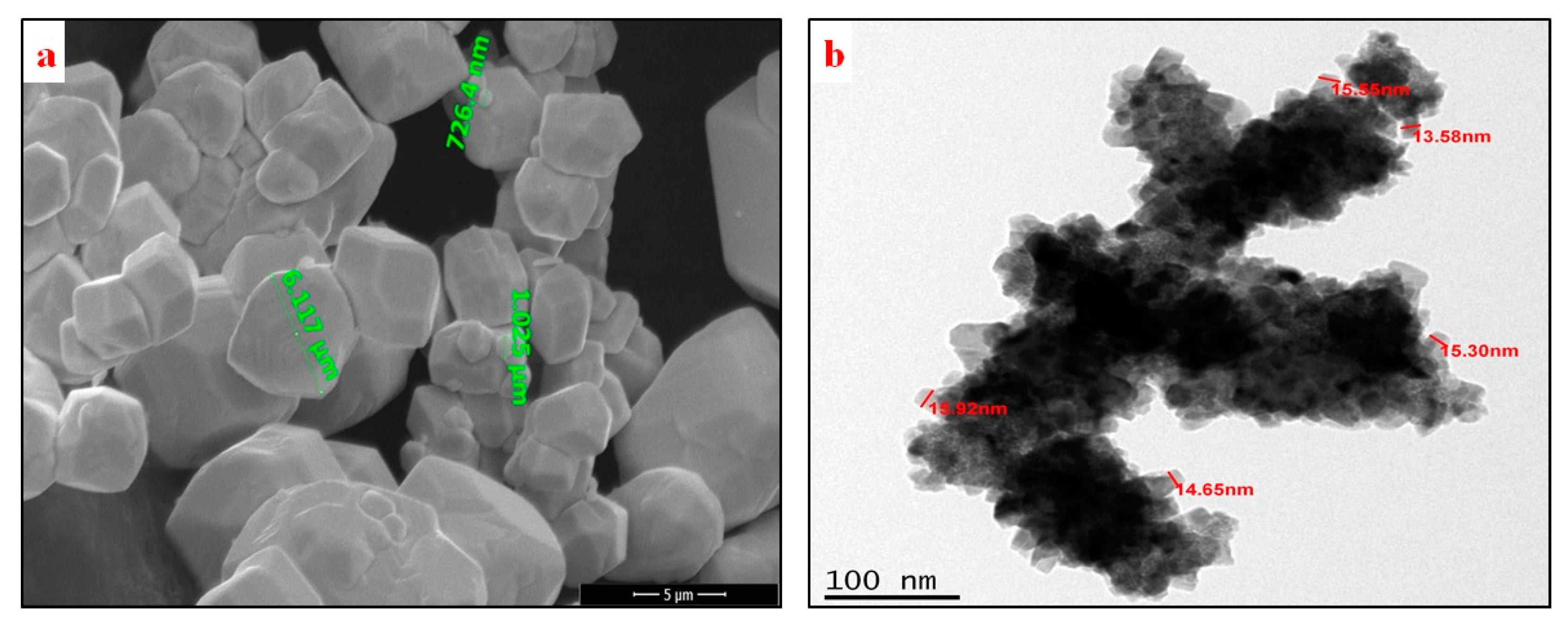
3.2. X-ray Diffraction (XRD)
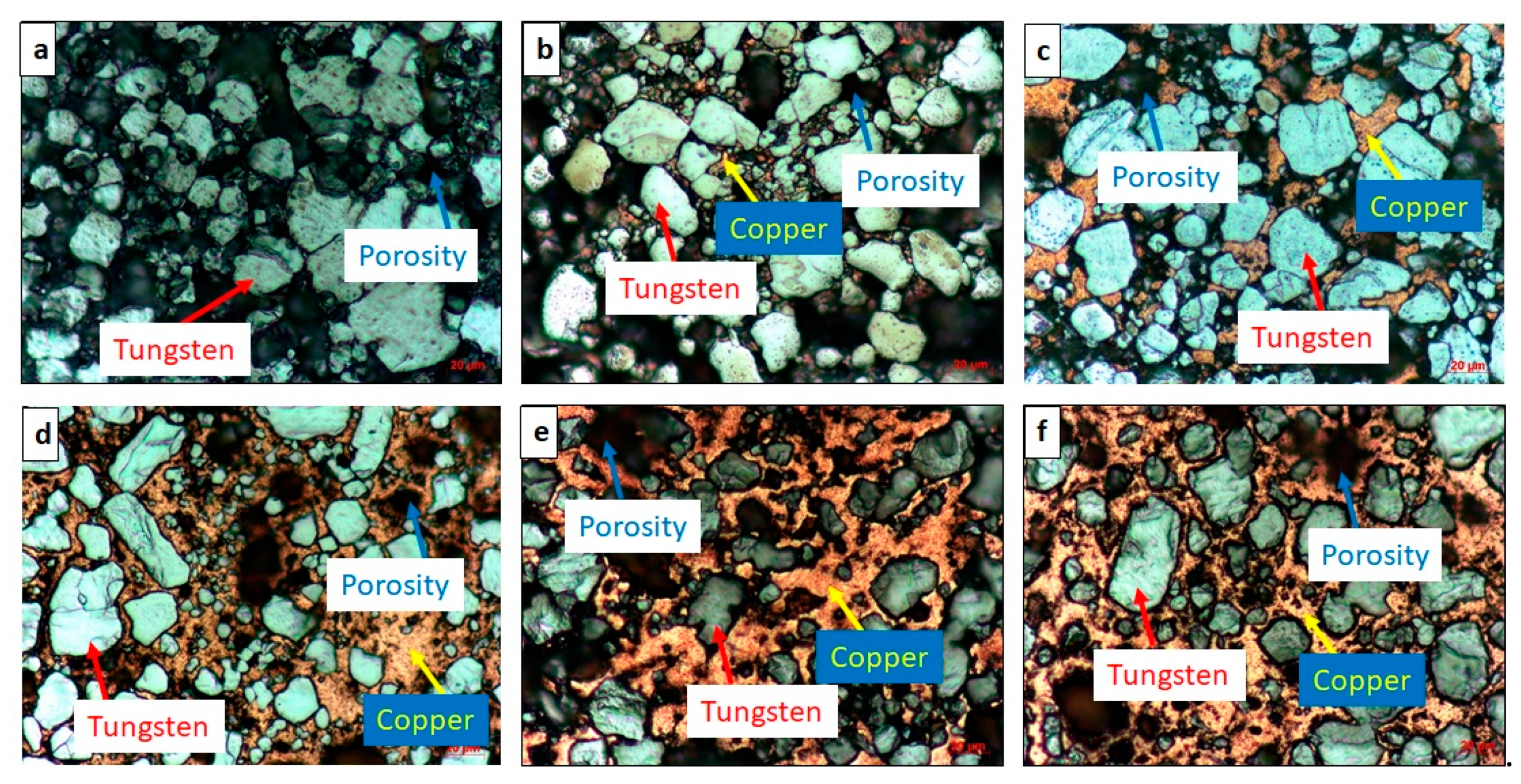
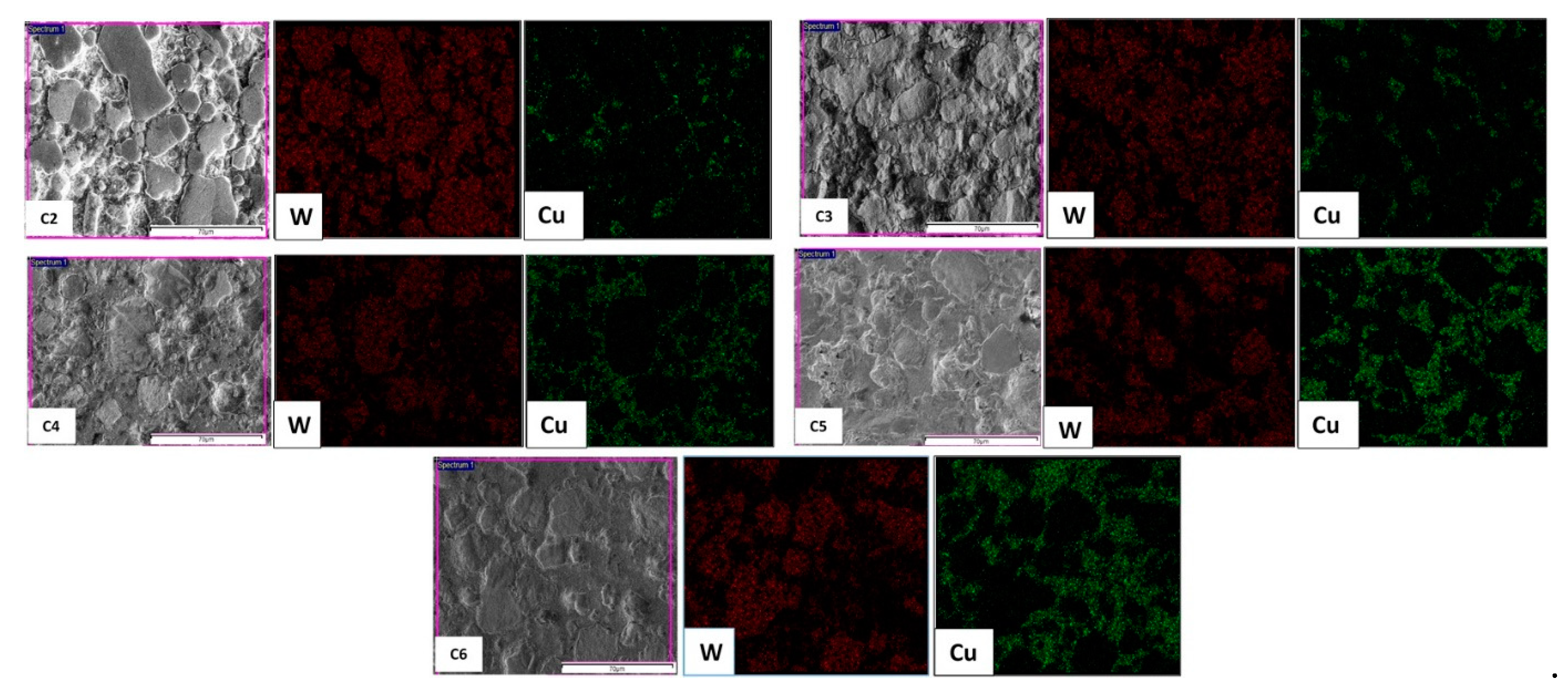
3.3. Microstructure
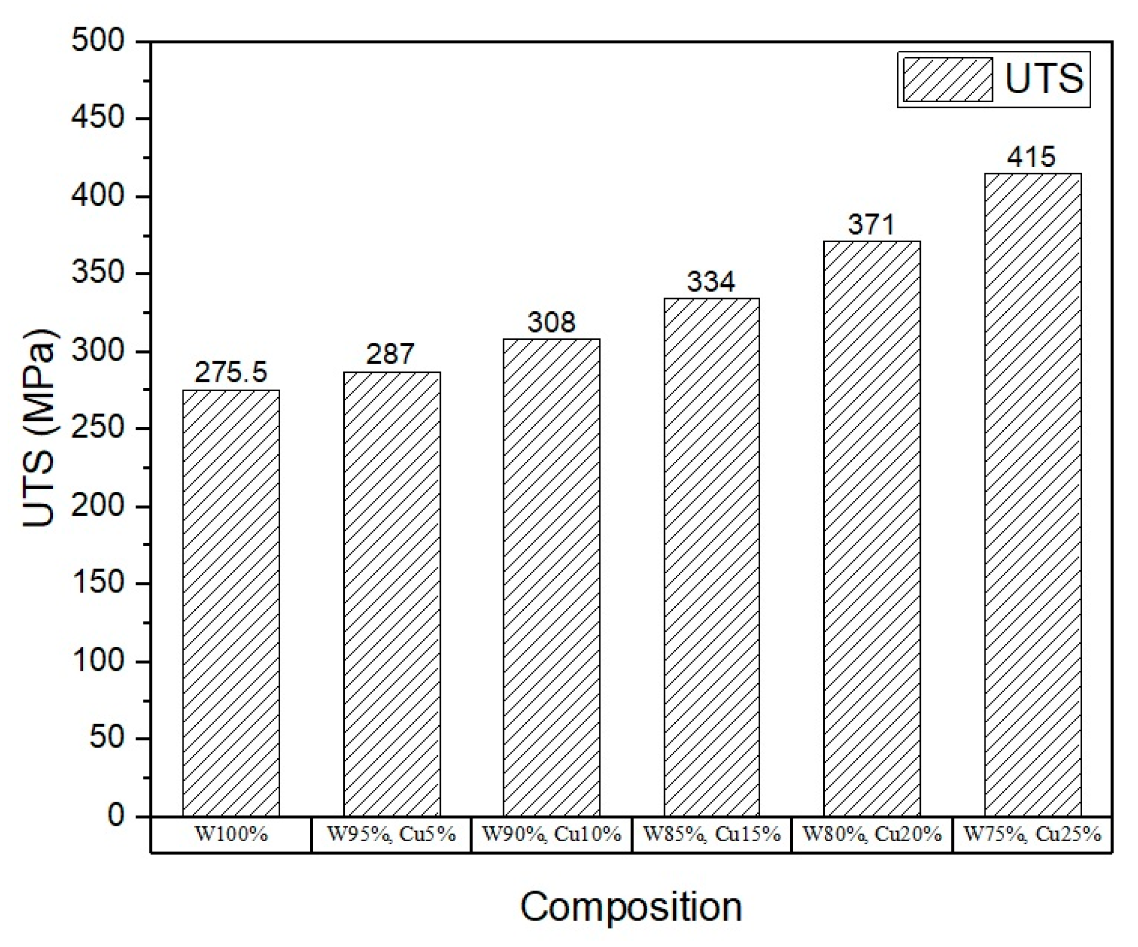
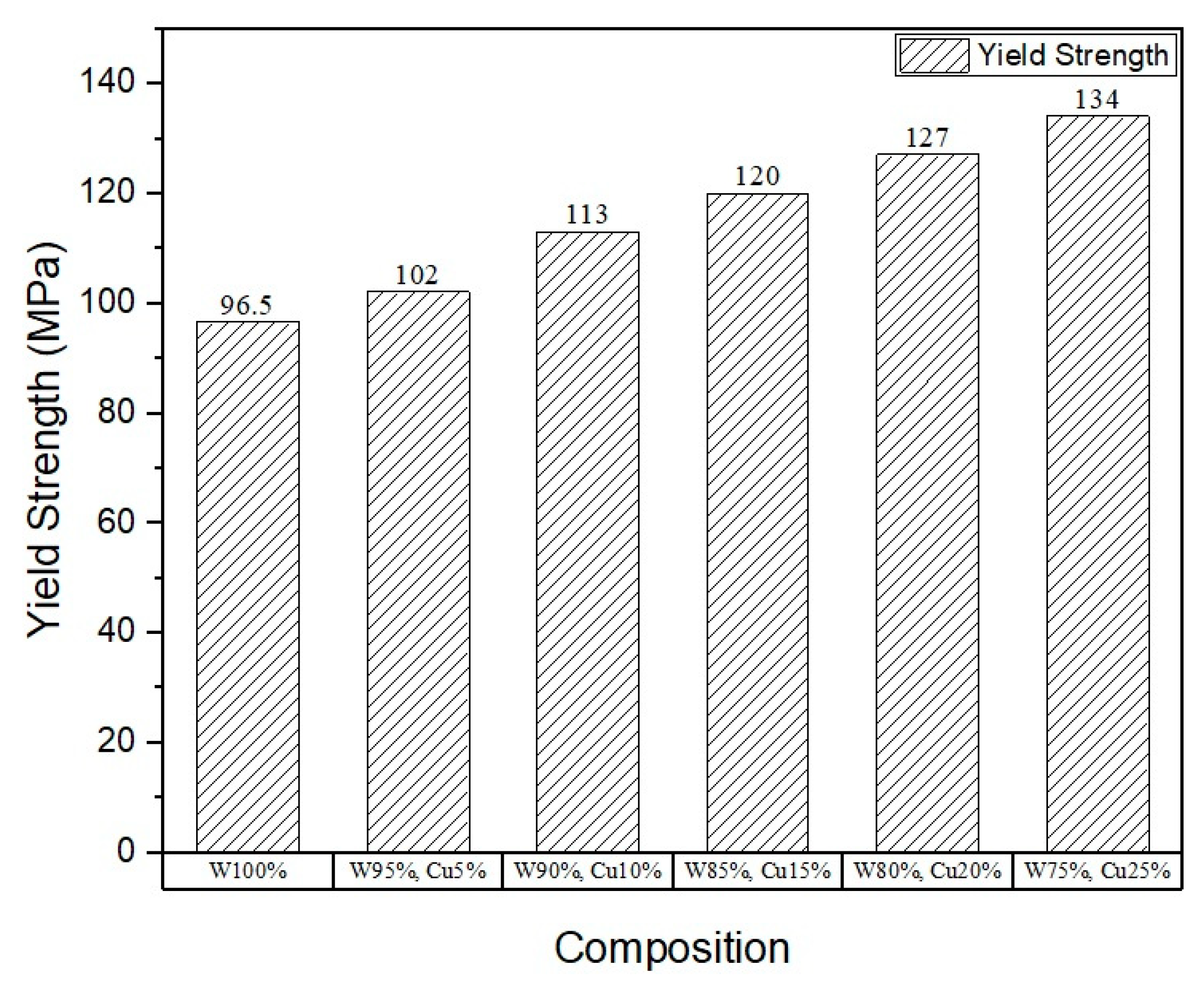
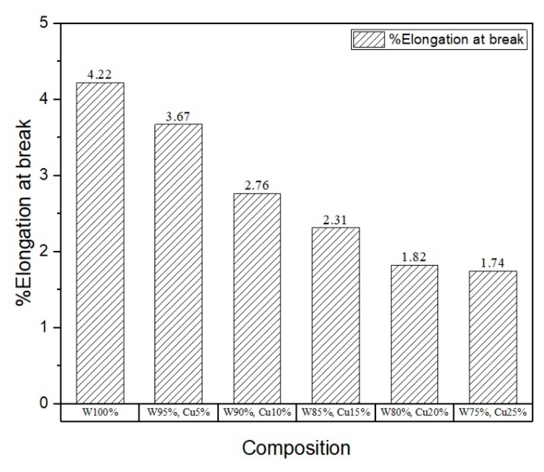
3.4. Mechanical Properties (Behavior)
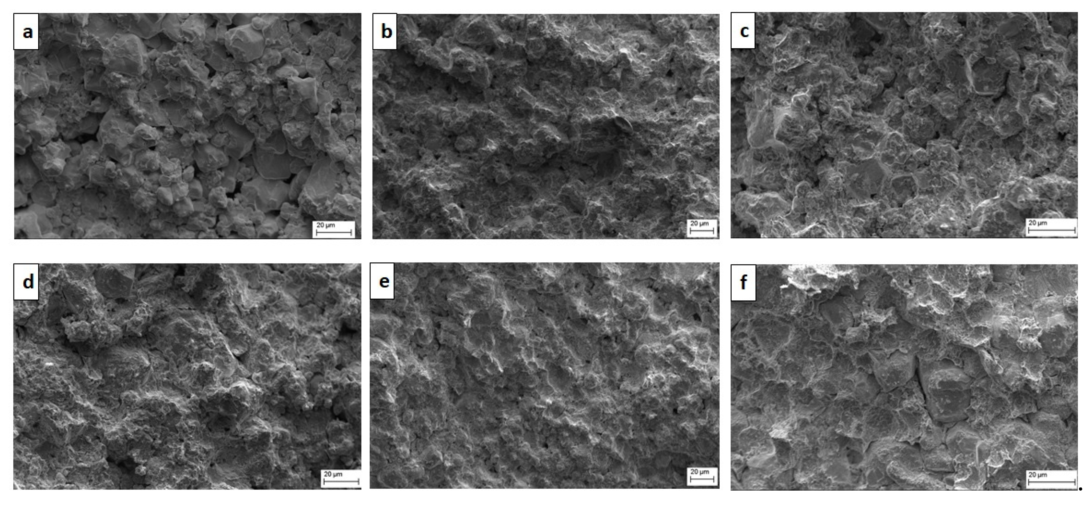
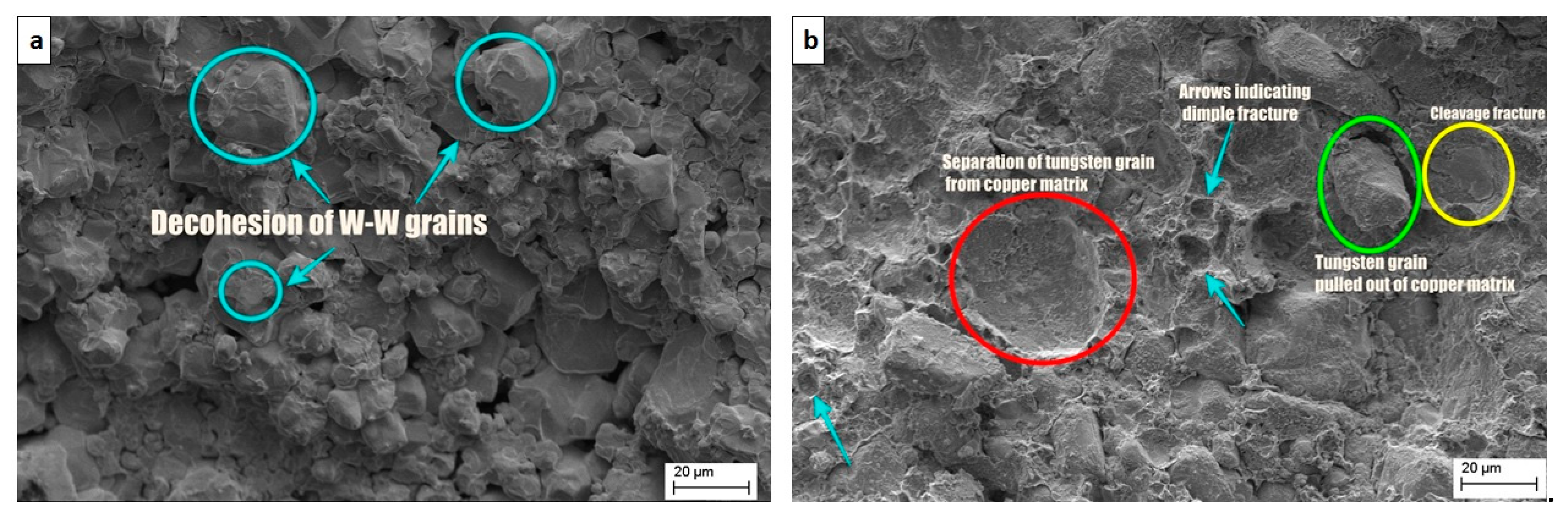
3.5. Fractography
3.6. Electrical Conductivity
4. Conclusions
Author Contributions
Funding
Institutional Review Board Statement
Informed Consent Statement
Data Availability Statement
Acknowledgments
Conflicts of Interest
References
- Doré, F.; Lay, S.; Eustathopoulos, N.; Allibert, C.H. Segregation of Fe during the sintering of doped W–Cu alloys. Scr. Mater. 2003, 49, 237–242. [Google Scholar] [CrossRef]
- Xu, L.; Yan, M.; Xia, Y.; Peng, J.; Li, W.; Zhang, L.; Liu, C.; Chen, G.; Li, Y. Influence of copper content on the property of Cu–W alloy prepared by microwave vacuum infiltration sintering. J. Alloy. Compd. 2014, 592, 202–206. [Google Scholar] [CrossRef]
- Qiu, W.T.; Pang, Y.; Xiao, Z.; Li, Z. Preparation of W-Cu alloy with high Density and ultrafine grains by mechanical alloying and high-pressure sintering. Int. J. Refract. Met. Hard Mater. 2016, 61, 91–97. [Google Scholar] [CrossRef]
- Chaubey, A.K.; Gupta, R.; Kumar, R.; Verma, B.; Kanpara, S.; Bathula, S.; Khirwadkar, S.S.; Dhar, A. Fabrication and characterization of W-Cu functionally graded material by spark plasma sintering process. Fusion Eng. Des. 2018, 135, 24–30. [Google Scholar] [CrossRef]
- Zhu, X.; Cheng, J.; Chen, P.; Wei, B.; Gao, Y.; Gao, D. Preparation and characterization of nanosized W-Cu powders by a novel solution combustion and hydrogen reduction method. J. Alloy. Compd. 2019, 793, 352–359. [Google Scholar] [CrossRef]
- Kwon, Y.S.; Chung, S.T.; Lee, S.; Noh, J.W.; Park, S.J.; German, R.M. Development of the High-Performance W-Cu Electrode. Adv. Powder Metall. Part. Mater. 2007, 2, 9. [Google Scholar]
- Hiraoka, Y.; Inoue, T.; Hanado, H.; Akiyoshi, N. Ductile-to-brittle transition characteristics in W–Cu composites with an increase of Cu content. Mater. Trans. 2005, 46, 1663–1670. [Google Scholar] [CrossRef] [Green Version]
- Ryu, S.S.; Kim, Y.D.; Moon, I.H. Dilatometric analysis on the sintering behavior of nanocrystalline W–Cu prepared by mechanical alloying. J. Alloy. Compd. 2002, 335, 233–240. [Google Scholar] [CrossRef]
- Wang, W.S.; Hwang, K.S. The effect of tungsten particle size on the processing and properties of infiltrated W-Cu compacts. Metall. Mater. Trans. A 1998, 29, 1509–1516. [Google Scholar] [CrossRef]
- Mordike, B.L.; Kaczmar, J.; Kielbinski, M.; Kainer, K.U. Effect of tungsten content on the properties and structure of cold extruded Cu-W composite materials. PMI. Powder Metall. Int. 1991, 23, 91–95. [Google Scholar]
- Ho, P.W.; Li, Q.F.; Fuh, J.Y.H. Evaluation of W–Cu metal matrix composites produced by powder injection molding and liquid infiltration. Mater. Sci. Eng. A 2008, 485, 657–663. [Google Scholar] [CrossRef]
- Amirjan, M.; Zangeneh-Madar, K.; Parvin, N. Evaluation of microstructure and contiguity of W/Cu composites prepared by coated tungsten powders. Int. J. Refract. Met. Hard Mater. 2009, 27, 729–733. [Google Scholar] [CrossRef]
- Ibrahim, A.; Abdallah, M.; Mostafa, S.F.; Hegazy, A.A. An experimental investigation on the W–Cu composites. Mater. Des. 2009, 30, 1398–1403. [Google Scholar] [CrossRef]
- Hamidi, A.G.; Arabi, H.; Rastegari, S. Tungsten–copper composite production by activated sintering and infiltration. Int. J. Refract. Met. Hard Mater. 2011, 29, 538–541. [Google Scholar] [CrossRef]
- Mondal, A.; Upadhyaya, A.; Agrawal, D. Comparative study of densification and microstructural development in W–18Cu composites using microwave and conventional heating. Mater. Res. Innov. 2010, 14, 355–360. [Google Scholar] [CrossRef]
- Pintsuk, G.; Brünings, S.E.; Döring, J.E.; Linke, J.; Smid, I.; Xue, L. Development of W/Cu—functionally graded materials. Fusion Eng. Des. 2003, 66, 237–240. [Google Scholar] [CrossRef]
- Johnson, J.L.; Brezovsky, J.J.; German, R.M. Effects of tungsten particle size and copper content on densification of liquid-phase-sintered W-Cu. Metall. Mater. Trans. A 2005, 36, 2807–2814. [Google Scholar] [CrossRef]
- Wei, X.; Tang, J.; Ye, N.; Zhuo, H. A novel preparation method for W–Cu composite powders. J. Alloy. Compd. 2016, 661, 471–475. [Google Scholar] [CrossRef]
- Huang, L.M.; Luo, L.M.; Ding, X.Y.; Luo, G.N.; Zan, X.; Cheng, J.G.; Wu, Y.C. Effects of simplified pretreatment process on the morphology of W–Cu composite powder prepared by electroless plating and its sintering characterization. Powder Technol. 2014, 258, 216–221. [Google Scholar] [CrossRef]
- Li, C.; Zhou, Y.; Xie, Y.; Zhou, D.; Zhang, D. Effects of milling time and sintering temperature on structural evolution, densification behavior, and properties of a W-20 wt. % Cu alloy. J. Alloy. Compd. 2018, 731, 537–545. [Google Scholar] [CrossRef]
- Mondal, A.; Upadhyaya, A.; Agrawal, D. Effect of heating mode and copper content on the densification of W-Cu alloys. Indian J. Mater. Sci. 2013, 2013, 1–7. [Google Scholar] [CrossRef]
- Zhanlei, W.; Huiping, W.; Zhonghua, H.; Hongyu, X.; Yifan, L. Dynamic consolidation of W-Cu nano-alloy and its performance as liner materials. Rare Met. Mater. Eng. 2014, 43, 1051–1055. [Google Scholar] [CrossRef]
- Zhang, N.; Wang, Z.; Guo, L.; Meng, L.; Guo, Z. Rapid fabrication of W–Cu composites via low-temperature infiltration in supergravity fields. J. Alloy. Compd. 2019, 809, 151782. [Google Scholar] [CrossRef]
- Guillon, O.; Gonzalez-Julian, J.; Dargatz, B.; Kessel, T.; Schierning, G.; Räthel, J.; Herrmann, M. Field-assisted sintering technology/spark plasma sintering: Mechanisms, materials, and technology developments. Adv. Eng. Mater. 2014, 16, 830–849. [Google Scholar] [CrossRef]
- Suárez, M.; Fernández, A.; Menéndez, J.L.; Torrecillas, R.; Kessel, H.U.; Hennicke, J.; Kirchner, R.; Kessel, T. Challenges and opportunities for spark plasma sintering: A key technology for a new generation of materials. Sinter. Appl. 2013, 13, 319–342. [Google Scholar]
- ASTM International. Standard Practice for Microetching Metals and Alloys; ASTM International E407-07; ASTM International: West Conshohocken, PA, USA, 2015. [Google Scholar]
- ASTM International. Standard Test Methods for Vickers Hardness and Knoop Hardness of Metallic Materials; ASTM International E92; ASTM International: West Conshohocken, PA, USA, 2017. [Google Scholar]
- ASTM International. Standard Test Method for Determining Electrical Conductivity Using the Electromagnetic (Eddy Current) Method; ASTM International E1004; ASTM International: West Conshohocken, PA, USA, 2017. [Google Scholar]
- Liang, S.; Wang, X.; Wang, L.; Cao, W.; Fang, Z. Fabrication of CuW pseudo alloy by W–CuO nanopowders. J. Alloy. Compd. 2012, 516, 161–166. [Google Scholar] [CrossRef]
- George, E.D. Mechanical Metallurgy, 2nd ed.; McGraw Hill Education: New York, NY, USA, 1976. [Google Scholar]
- Chen, P.; Shen, Q.; Luo, G.; Wang, C.; Li, M.; Zhang, L.; Li, X.; Zhu, B. Effect of interface modification by Cu-coated W powders on the microstructure evolution and properties improvement for Cu–W composites. Surf. Coat. Technol. 2016, 288, 8–14. [Google Scholar] [CrossRef]
- Liang, S.; Chen, L.; Yuan, Z.; Li, Y.; Zou, J.; Xiao, P.; Zhuo, L. Infiltrated W–Cu composites with the combined architecture of hierarchical particulate tungsten and tungsten fibers. Mater. Charact. 2015, 110, 33–38. [Google Scholar] [CrossRef]


| Composition (wt.%). | Relative Density (%) | Notation |
|---|---|---|
| W100% | 69.76 | C1 |
| W95%Cu5% | 71.89 | C2 |
| W90%Cu10% | 77.34 | C3 |
| W85%Cu15% | 79.91 | C4 |
| W80%Cu20% | 81.43 | C5 |
| W75%Cu25%. | 82.26 | C6 |
| Composition. | Grain Size (µm) |
|---|---|
| W100% | 20 ± 2 |
| W95%, Cu5% | 19 ± 2 |
| W90%, Cu10% | 18 ± 1 |
| W85%, Cu15% | 16 ± 1 |
| W80%, Cu20% | 16 ± 1 |
| W75%, Cu25% | 15 ± 1 |
Publisher’s Note: MDPI stays neutral with regard to jurisdictional claims in published maps and institutional affiliations. |
© 2021 by the authors. Licensee MDPI, Basel, Switzerland. This article is an open access article distributed under the terms and conditions of the Creative Commons Attribution (CC BY) license (http://creativecommons.org/licenses/by/4.0/).
Share and Cite
Madhur, V.; Srikanth, M.; Annamalai, A.R.; Muthuchamy, A.; Agrawal, D.K.; Jen, C.-P. Effect of Nano Copper on the Densification of Spark Plasma Sintered W–Cu Composites. Nanomaterials 2021, 11, 413. https://0-doi-org.brum.beds.ac.uk/10.3390/nano11020413
Madhur V, Srikanth M, Annamalai AR, Muthuchamy A, Agrawal DK, Jen C-P. Effect of Nano Copper on the Densification of Spark Plasma Sintered W–Cu Composites. Nanomaterials. 2021; 11(2):413. https://0-doi-org.brum.beds.ac.uk/10.3390/nano11020413
Chicago/Turabian StyleMadhur, Vadde, Muthe Srikanth, A. Raja Annamalai, A. Muthuchamy, Dinesh K. Agrawal, and Chun-Ping Jen. 2021. "Effect of Nano Copper on the Densification of Spark Plasma Sintered W–Cu Composites" Nanomaterials 11, no. 2: 413. https://0-doi-org.brum.beds.ac.uk/10.3390/nano11020413