Article

High-Performance On-Chip Silicon Beamsplitter Based on Subwavelength Metamaterials for Enhanced Fabrication Tolerance

by
Raquel Fernández de Cabo
1,*,
David González-Andrade
1,
Pavel Cheben
2 and
Aitor V. Velasco
1
1
Instituto de Óptica Daza de Valdés, Consejo Superior de Investigaciones Científicas (CSIC), 28006 Madrid, Spain
2
National Research Council Canada, Ottawa, ON K1A 0R6, Canada
*
Author to whom correspondence should be addressed.
Submission received: 19 April 2021 / Revised: 12 May 2021 / Accepted: 13 May 2021 / Published: 14 May 2021
(This article belongs to the Special Issue Silicon Photonics: Synthesis and Applications)

Abstract

:
Efficient power splitting is a fundamental functionality in silicon photonic integrated circuits, but state-of-the-art power-division architectures are hampered by limited operational bandwidth, high sensitivity to fabrication errors or large footprints. In particular, traditional Y-junction power splitters suffer from fundamental mode losses due to limited fabrication resolution near the junction tip. In order to circumvent this limitation, we propose a new type of high-performance Y-junction power splitter that incorporates subwavelength metamaterials. Full three-dimensional simulations show a fundamental mode excess loss below 0.1 dB in an ultra-broad bandwidth of 300 nm (1400–1700 nm) when optimized for a fabrication resolution of 50 nm, and under 0.3 dB in a 350 nm extended bandwidth (1350–1700 nm) for a 100 nm resolution. Moreover, analysis of fabrication tolerances shows robust operation for the fundamental mode to etching errors up to ±20 nm. A proof-of-concept device provides an initial validation of its operation principle, showing experimental excess losses lower than 0.2 dB in a 195 nm bandwidth for the best-case resolution scenario (i.e., 50 nm).

1. Introduction

The silicon-on-insulator (SOI) integrated photonic platform has been successfully exploited in a wide variety of fields, from telecom and datacom systems [1,2] to biochemical sensors [3], LIDAR systems [4], microspectrometers [5,6,7] and supercontinuum generation [8], among many others. The expansion into these diverse application fields has been made possible by the inherent benefits of the SOI platform, including large capacity of integration due to high refractive-index contrast [9] and low-cost mass production provided by the compatibility with complementary metal oxide semiconductor (CMOS) fabrication processes [10]. Conversely, the strong modal confinement results in SOI devices with high sensitivity to geometrical deviations from nominal design. This constraint is also present in power splitting components, a fundamental functionality in most silicon photonic integrated circuits [11] and, specifically, in an extensive range of applications including wavelength- and mode-division multiplexing [12], optical phased arrays [13] and on-chip spectrometers [6].
State-of-the-art power division structures such as directional couplers, multimode interference (MMI) devices or power splitters based on slot and adiabatic waveguides entail shortcomings in terms of reduced operational bandwidth, high sensitivity to fabrication deviations or large footprints [14,15,16,17,18,19,20,21]. Directional couplers [14], despite a significant improvement in their manufacturing tolerances through geometrical optimization [15] and phase control sections [16], still present comparatively limited operational bandwidth. While bent directional couplers [17] have achieved a broadband response, they are affected by a strong sensitivity to manufacturing deviations. Slot waveguides [18] and adiabatic couplers [19] have demonstrated good performance over a wide bandwidth; however, these devices have considerably larger footprints. Similarly, MMI couplers offer numerous advantages, such as relatively small size and relaxed manufacturing tolerances [20], but their bandwidth is limited by the strong modal dispersion in multimode SOI waveguides. Different structures have also been proposed for power splitting, including inverse tapers [21], adiabatic tapers [22] and photonic crystals [23], which are limited by their narrow bandwidth.
Symmetric Y-junctions, consisting of a stem waveguide which branches into two diverging arms, are one of the most widely used power splitters and belong to the very roots of integrated optics. Y-junction studies were first conducted in the 1970s [24,25], with the first cascaded 1 × 8 power splitters being presented on ion-exchanged glass in the 1980s [26]. Nowadays, Y-junctions are routinely incorporated, for example, in ultra-high speed, high-quality lithium niobate electro-optic modulators [27]. Due to the simplicity of its design and operation principle [28,29], we consider these devices to be of special interest for SOI platforms, particularly for applications involving cascaded power splitting (e.g., integrated microspectrometers [30]. Moreover, Y-junctions with a bimodal stem waveguide offer a strong potential in datacom applications of growing interest, such as mode division multiplexing [12,31,32]. The transition between the stem and arms is nearly lossless and wavelength independent for small enough branching angles and a perfectly sharp junction tip between said branches [28]. However, the latter condition is hindered in real scenarios by the finite resolution of fabrication processes, hence requiring the application of more complex structures and optimization algorithms, such as slotted Y-junctions [18] or particle swarm optimization (PSO) [33]. This is particularly stringent in deep-ultraviolet (UV) lithography [34], with a substantially larger minimum feature size (MFS) compared to electron-beam (e-beam) technology. Moreover, since the junction tip is located at the midpoint of the stem waveguide, coinciding with the fundamental mode power maximum, deviations from the tip nominal design particularly penalize losses for the fundamental mode. Conversely, first-order modes present a zero-power profile at their central point, enabling power lobe separation without significant losses.
Subwavelength grating (SWG) metamaterials, since their first demonstration in silicon waveguides [35,36,37,38,39,40], have been advantageously used as a powerful tool for overcoming performance limitations of conventional silicon-based integrated photonic devices [41,42]. SWGs are periodic arrangements of different dielectric materials with a grating period (Λ) substantially smaller than the wavelength (λ) of the propagating light [43]. Under this condition, the medium acts on a macroscopic level as a homogeneous metamaterial which combines the optical properties of its dielectric constituents (e.g., effective index, dispersion, anisotropy), hence enabling the customization of the medium optical response through geometrical design. This innovative solution has been successfully applied to fiber-chip couplers, on-chip polarization management, mode-division multiplexing and integrated interferometer arrays, to name a few examples [6,12,44]. Specifically, subwavelength metamaterials have been applied to different power splitting architectures such as directional couplers [45,46,47] or MMIs [48,49], providing compact devices with enhanced performance over a broad bandwidth [50].
In this work, we incorporate an SWG metamaterial in a symmetric Y-junction to effectively reduce mode confinement around the junction tip and, hence, mitigate fundamental mode loss penalty caused by MFS limitations. Two different resolution scenarios have been taken into account for the optimization of the SWG Y-junction: (i) with an MFS of 100 nm, corresponding to current deep-UV fabrication process (dry lithography) and (ii) with an MFS of 50 nm for emerging high-resolution processes in photonic foundries (immersion lithography). Full three-dimensional finite-difference time-domain (3D FDTD) simulations show negligible fundamental mode excess losses (EL) within an ultra-broad bandwidth in excess of 300 nm for both MFS scenarios. In addition, our device presents robust fabrications tolerances to over- and under-etching deviations of up to ±20 nm. A proof-of-concept device was fabricated, showing experimental excess losses lower than 0.2 dB in a 195 nm bandwidth for the best-case resolution scenario.

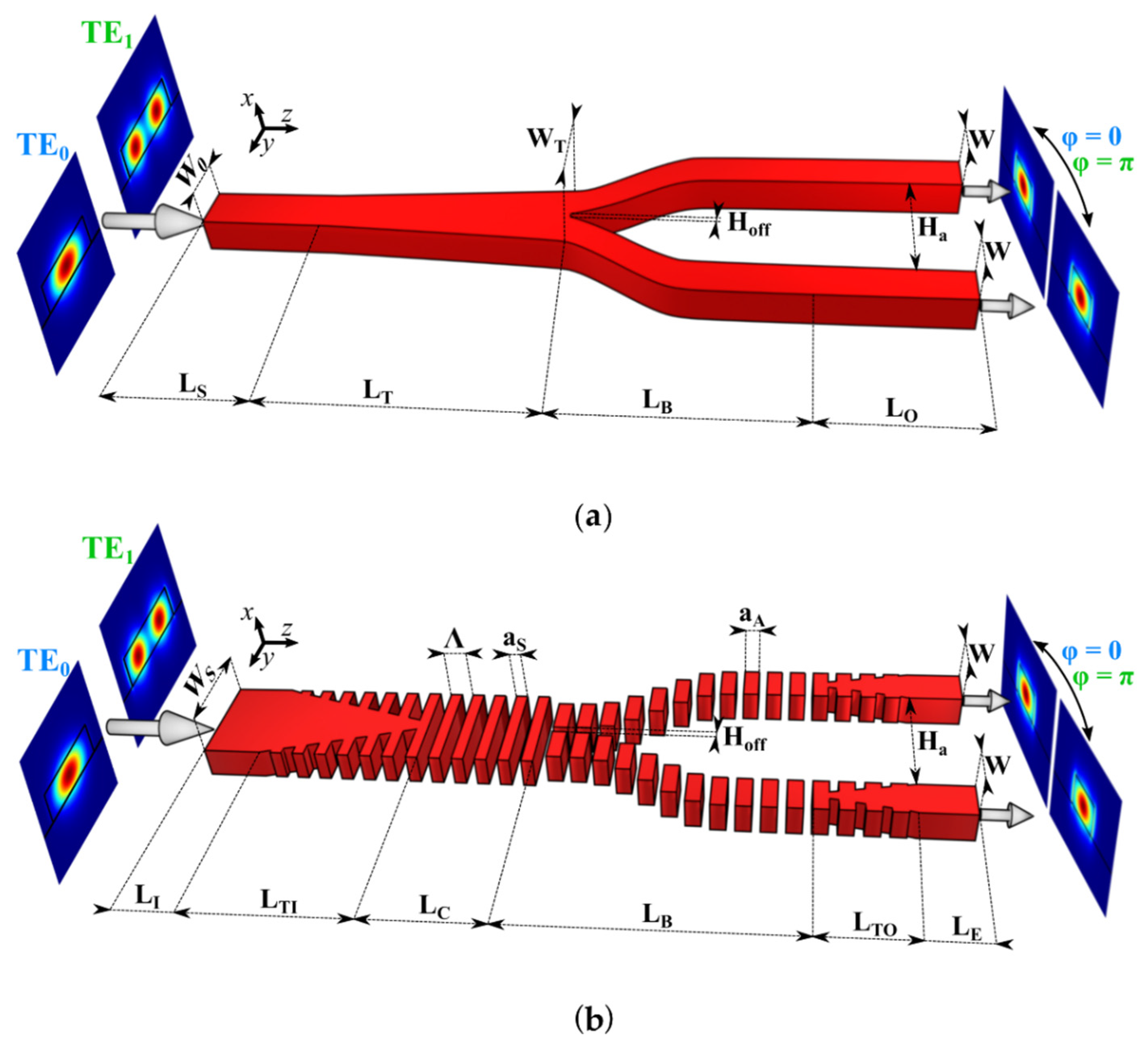
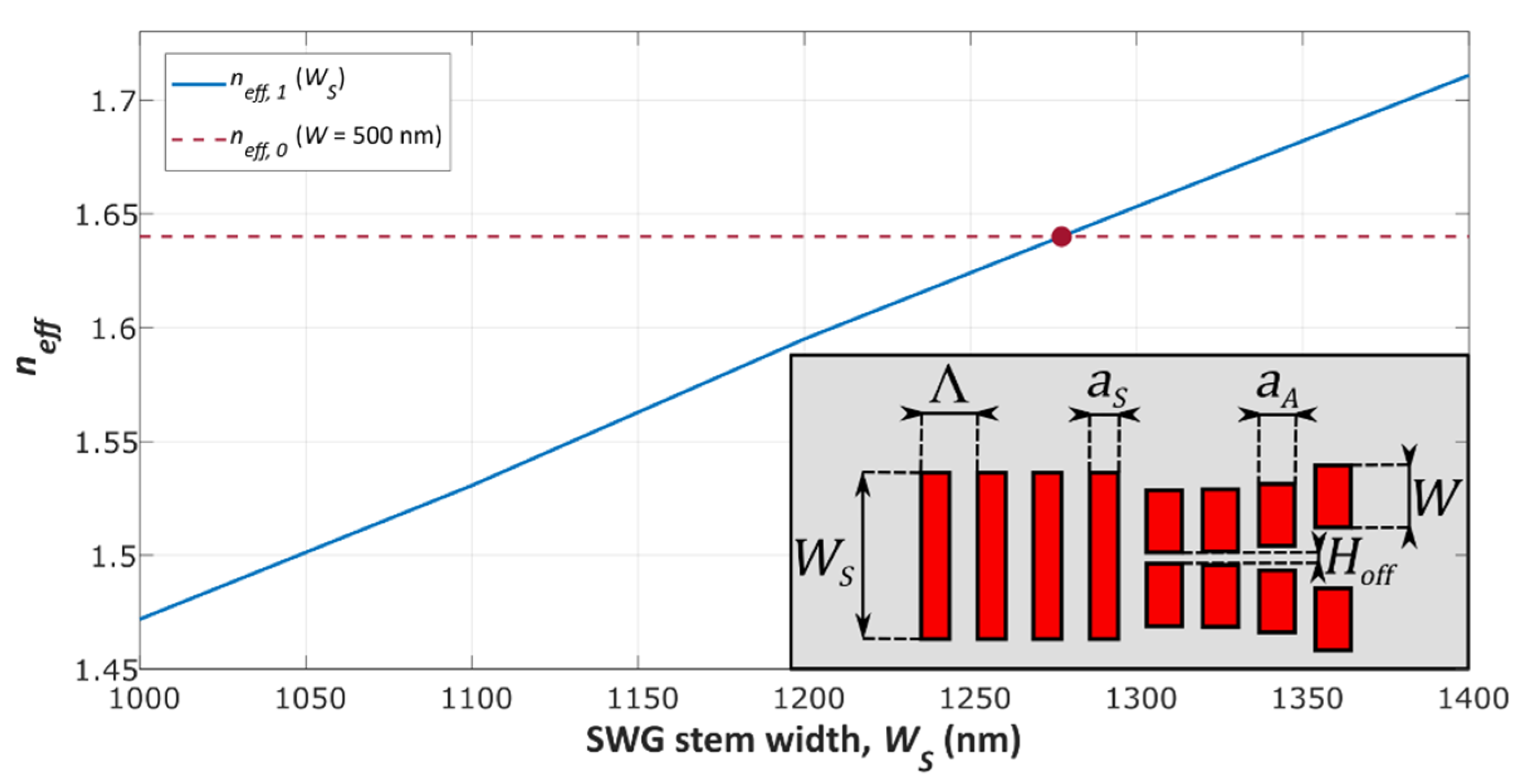
2. Principle of Operation and Device Design

As a reference framework for our proposed device, let us first consider a conventional symmetric Y-junction as depicted in Figure 1a, operating for fundamental and first-order transverse electric (TE) modes. The device comprises an input multimode waveguide (stem) of width W0 and length Ls, and two single-mode S-shaped output arms of width W = W0/2, length LB and final separation Ha, followed by output straight waveguides of length LO. S-shaped waveguides are typically used to implement lateral displacements connecting two parallel straight waveguides due to their reduced losses [51]. An adiabatic taper of length LT is also included to adapt the stem waveguide to the width of both arms at the fork (WT = 2W + Hoff). When the divergence angle at the junction between the two arms is small enough to consider an adiabatic transition [28], the input fundamental TE mode (TE0) injected at the stem is divided into two in-phase TE0 modes at the output arms due to the symmetry of the device. Similarly, when the first-order TE mode (TE1) is injected, the power is again equally divided into two TE0 modes of equal amplitude at the output arms, but with a π phase difference (φ) between them. In order to account for the MFS constraint of the fabrication process, we consider a gap of width Hoff between the two arms at the junction tip.
Our proposed device, displayed in Figure 1b, operates analogously to a conventional symmetric Y-junction, but incorporates SWG metamaterials in both input and output waveguides, while preserving the same arm offset (Hoff). Arm width (W) and final separation (Ha) are maintained identical as in the conventional Y-splitter for the sake of comparison. The input strip waveguide of length LI and width WS evolves into an SWG waveguide of length LC through an adiabatic taper (length LTI). This SWG region is key to reduce the modal confinement of the TE0 mode and subsequently to minimize the radiation loss at the fork and improve its excess losses. Furthermore, the use of subwavelength structures allows to define geometrical parameters (period, duty cycle and Hoff) with larger values than the considered MFS (i.e., 50 nm and 100 nm). In order to minimize mode mismatch at the interface between the input stem and the output arms, we utilized different duty cycles on both sides, DCS = aS/Λ and DCA = aA/Λ, where aS and aA are the length of the silicon segments in the stem and in the arms, respectively, considering a constant period Λ.
The device was optimized for an SOI platform with a core waveguide thickness of 220 nm and both top and buried silicon dioxide layers. At a wavelength of 1550 nm, the material refractive indices were nSi ∼ 3.48 and nSiO2 ∼ 1.44. The device was simulated using a 3D FDTD solver [52] for two different fabrication resolution limits: 50 nm and 100 nm. Therefore, the parameter Hoff was modified accordingly to each MFS scenario. The width of the Y-junction arms was W = 500 nm, ensuring compatibility with conventional interconnection waveguides. An SWG period of Λ = 220 nm was selected to avoid radiation and Bragg regimes. The list of the remaining geometrical design parameters is provided in Table 1.
The width of the SWG stem waveguide was optimized to avoid a weak confinement of the Bloch–Floquet TE1 mode, which would lead to high TE1 excess losses (ELTE1) due to substrate leakage or mode radiation. TE1 mode splitting can be enhanced by selecting a wider SWG waveguide width, at the expense of a stronger confinement for the Bloch–Floquet TE0 mode and, therefore, higher TE0 excess losses (ELTE0). Figure 2 shows the effective index of the Bloch-Floquet TE1 mode (neff,1) supported by the SWG stem waveguide as a function of the waveguide width. The effective index of the Bloch–Floquet TE0 mode (neff,0) supported by the arms is also shown with a dashed red line. On this account, a width of the SWG stem waveguide of WS = 1200 nm was chosen as a compromise between ELTE0 and ELTE1.
To further optimize mode matching at the stem-arms interface, we judiciously adjusted the duty cycle on both parts of the device. For this purpose, we swept EL for different DCA while keeping a constant DCS of 50% (see Figure 3). We assumed two additional restrictions, i.e., that the chosen DCA cannot violate the MFS and that the optimum DCA values ELTE0 and ELTE1 may not necessarily be identical. For the MFS of 50 nm, the optimal loss balance for both TE0 and TE1 modes was achieved with a DCA = 60% (see Figure 3a). For the MFS of 100 nm, we found minimum EL for TE1 at DCA = 55% (see Figure 3b).

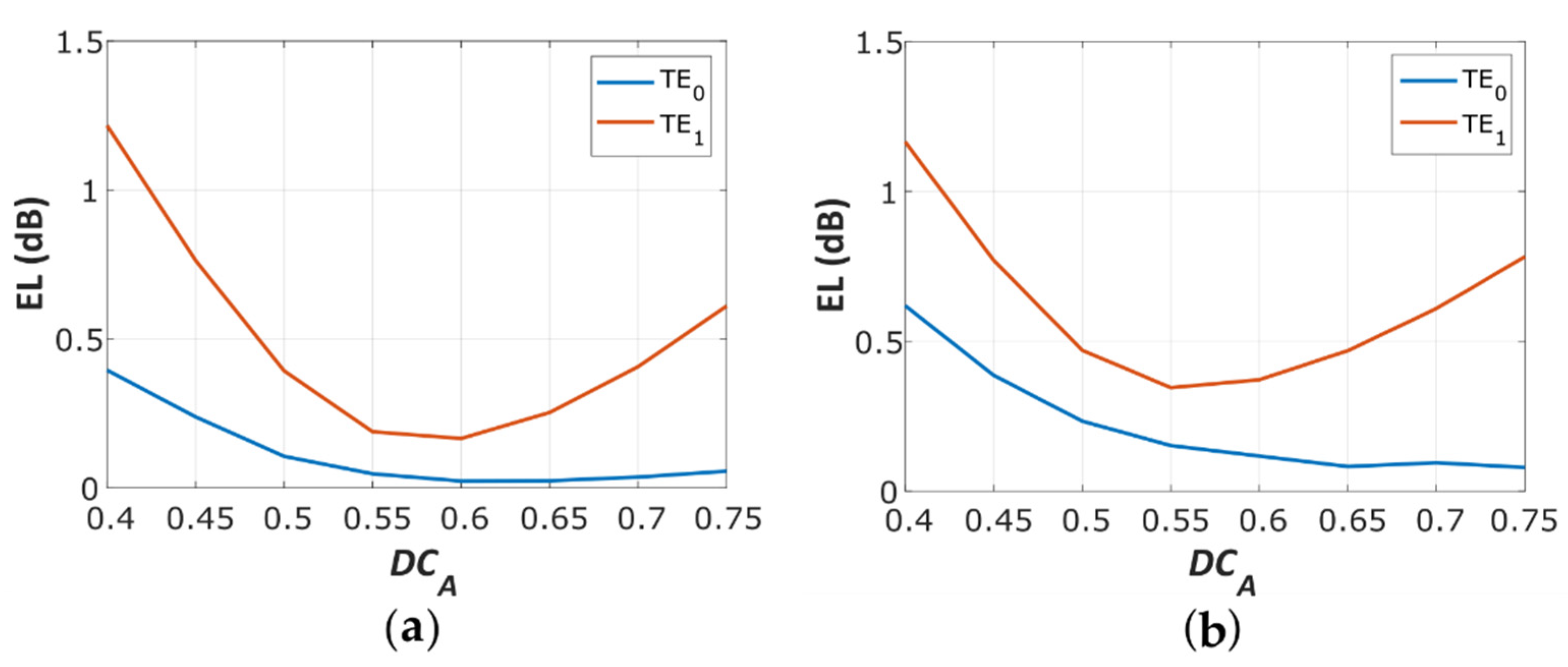
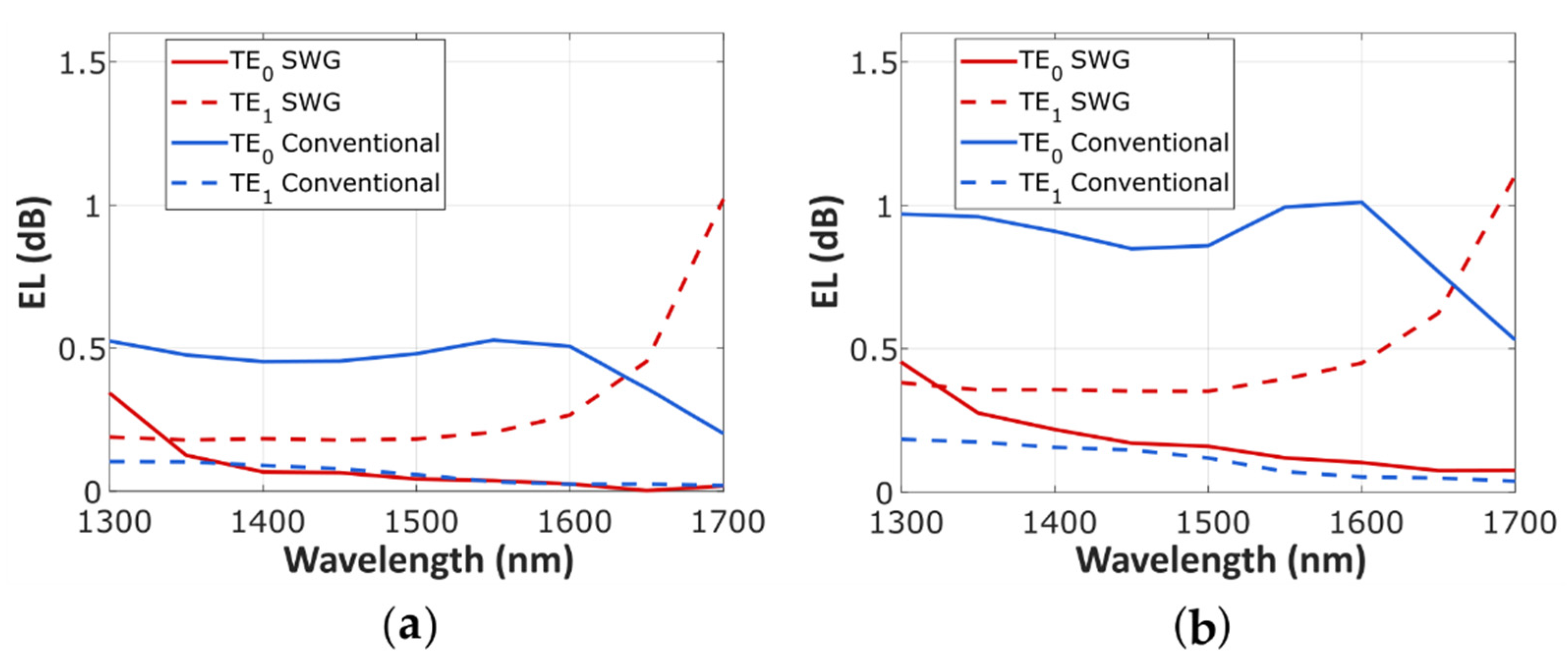
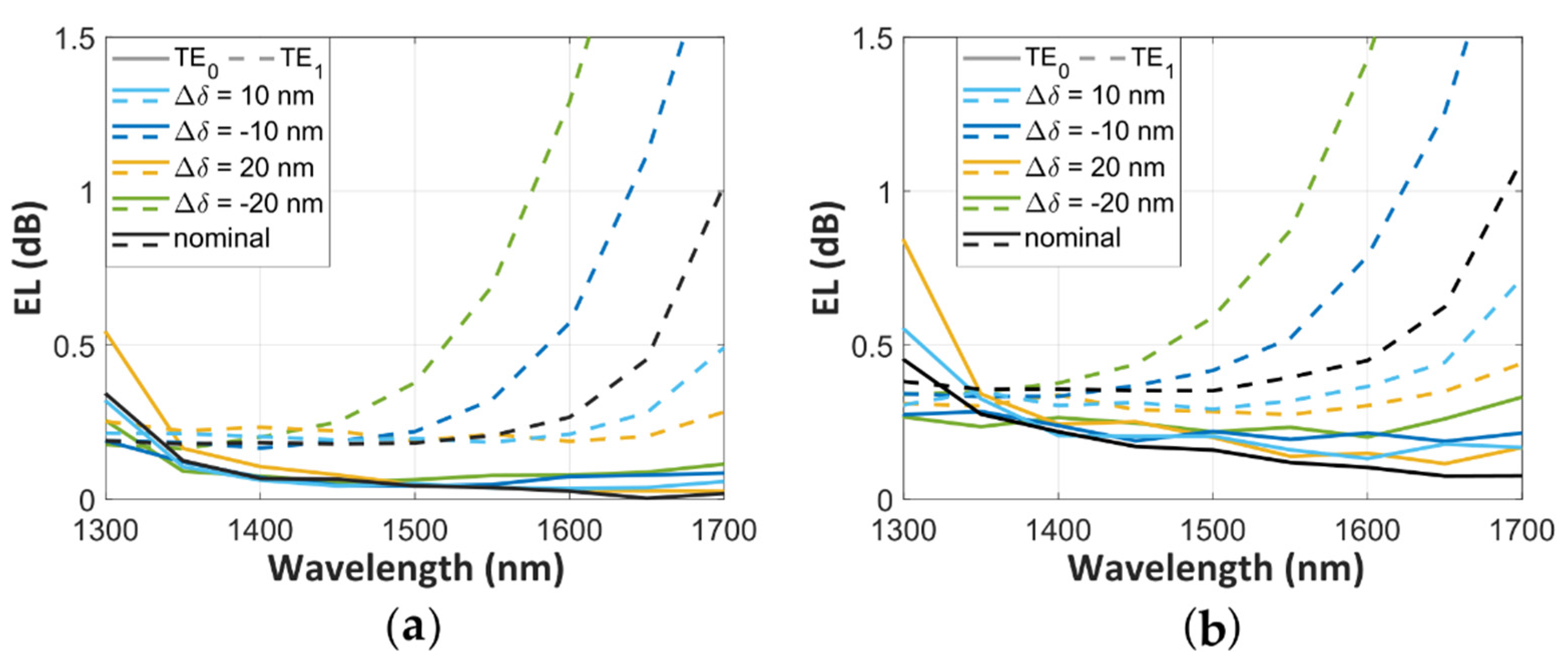
3. Simulation Results and Tolerance Analysis

The performance comparison between the optimized SWG Y-junction (red) and its conventional counterpart (blue) is shown in Figure 4 (ELTE0 solid curve, ELTE1 dashed curve). For an MFS of 50 nm (Figure 4a), our device shows an excellent performance in a broad bandwidth of 300 nm, with ELTE0 below 0.1 dB for a wavelength range from 1400 nm to 1700 nm, and under 0.3 dB for the TE1 mode in a 1300–1600 nm window. For comparison, ELTE0 is reduced by 0.35 dB compared to the conventional splitter in a 250 nm bandwidth (1350–1600 nm), while ELTE1 is only slightly increased. Considering the MFS of 100 nm (Figure 4b), the SWG Y-junction exhibits ELTE0 as low as 0.3 dB in a 350 nm bandwidth (1350–1700 nm) and ELTE1 under 0.45 dB in a 300 nm wavelength range (1300–1600 nm). A significant reduction for ELTE0 is achieved at the central design wavelength (1550 nm), from 0.99 dB for a conventional Y-junction down to 0.12 dB for the SWG Y-junction. Despite a minor increase in ELTE1, the sum of both EL values is significantly reduced for the SWG device compared to the conventional Y-junction, providing a more even performance for both modes, for both 100 nm and 50 nm MFS designs. This outstanding performance is achieved in a broad bandwidth of 300 nm (1300–1600 nm), with the ELTE0 + ELTE1 under 0.5 dB being the figure of merit. The SWG Y-junction shows improved performance for both 100 nm and 50 nm MFS designs, while the performance of the conventional Y-junction degrades rapidly with increasing MFS. Simulations also confirmed that the effect of temperature changes on device performance were negligible for variations of ±10 K for both modes (TE0 or TE1), as well as for the two MFS designs.
We also evaluated the fabrication tolerance of the SWG Y-junction to etching errors of Δδ = ± 10 nm and Δδ = ± 20 nm from our nominal design, as illustrated in Figure 5. For this purpose, we resized the whole device by adding to the length and width of the silicon segments the corresponding deviation, since we consider fabrication errors as absolute variations of the waveguide dimensions. Then, aS′ = aS + Δδ and aA= aA + Δδ are the lengths of the silicon segments at the stem and the arms of the SWG Y-junction, and the width at the stem and of the arms are WS= WS + Δδ and WA= W + Δδ, respectively. For both MFS values, i.e., 50 nm (Figure 5a) and 100 nm (Figure 5b), the SWG Y-junction performance degradation is observed predominantly for the TE1 mode when Δδ is negative, i.e., for over-etching errors. By contrast, the TE0 mode exhibits robust tolerances, particularly for the MFS = 50 nm.

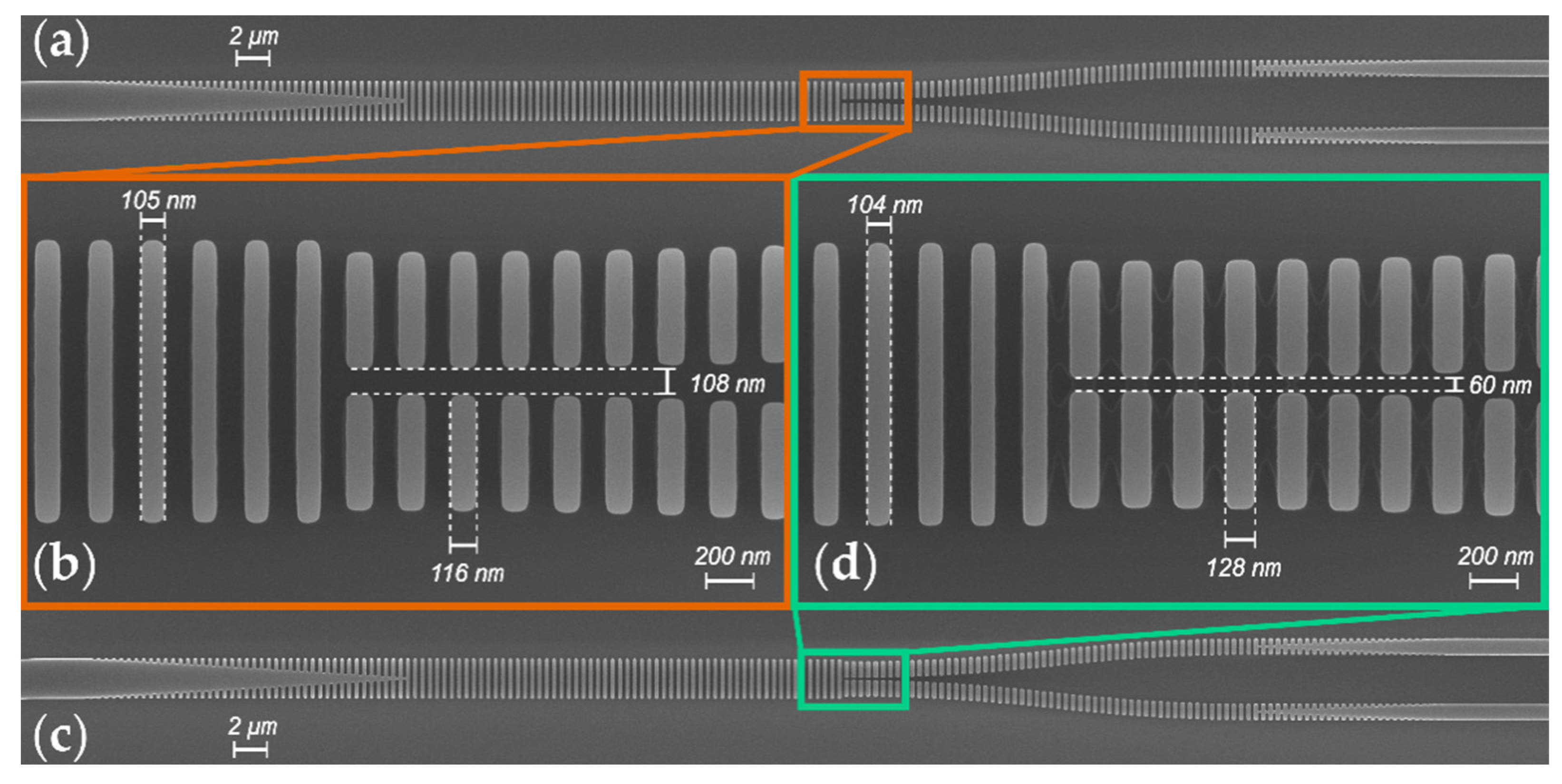
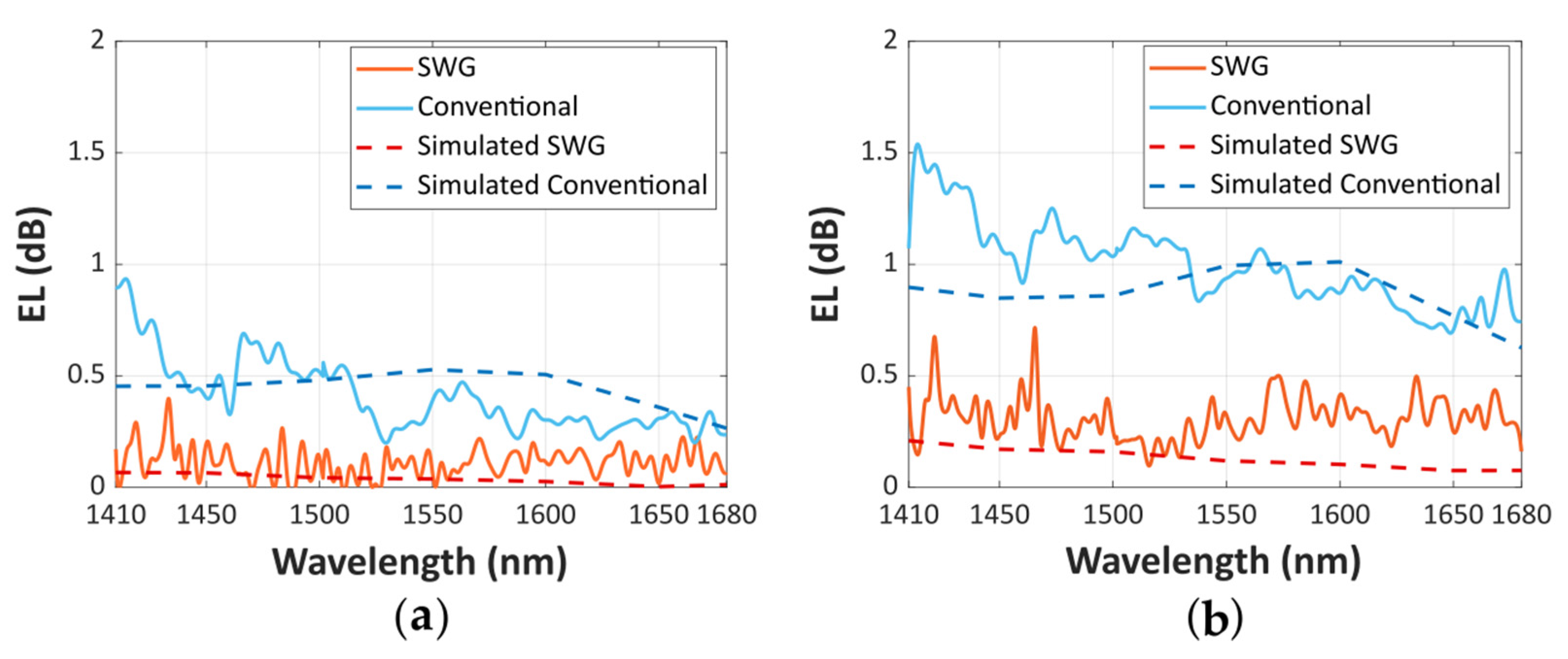
4. Fabrication and Experimental Characterization

A proof-of-concept device was fabricated using SOI wafers with the 220 nm thick Si layer and 2 µm thick buried oxide (BOX). E-beam lithography was used to define the pattern, and the 220 nm thick Si layer was fully etched by inductively coupled plasma reactive ion etching. A SiO2 upper cladding was deposited via chemical vapor deposition to protect the devices. Figure 6 shows the scanning electron microscope (SEM) images of the fabricated devices prior the cladding deposition. SEM image of the subwavelength Y-junction with an MFS of 100 nm is presented in Figure 6a, with a more detailed view of the tip in Figure 6b. Adhering to this previous arrangement, SEM images of the splitter with an MFS of 50 nm can be seen in Figure 6c,d. Detailed SEM image analysis shows a slight over etching, with deviations below Δδ < −10 nm in SWG segments of both arms and stem. A Mach-Zehnder interferometer (MZI) comprising two SWG Y-splitters was used to evaluate the coupler performance. High-efficiency and broadband SWG edge couplers [53,54] were used to couple the light in and out of the chip within the entire operational bandwidth of the device.
The fabricated device was characterized with two tunable lasers sweeping the wavelength range from 1.41 to 1.68 µm, fully covering the S, C, L and U telecom bands, and partially the E-band. Polarization at the chip input was controlled through a three-paddle fiber polarizer followed by a linear polarizer, a half-wave plate and a lensed polarization maintaining fiber. The polarization state was verified using a free-space polarimeter for the entire wavelength range (1.41–1.68 µm). The polarization state at the chip output was monitored with a Glan-Thompson polarizer, and a 40× microscope objective was used to focus the light onto a germanium photodetector. The difference between the transmittance of the measured MZI transmittance maxima and a reference waveguide, with the same waveguide length and number of bends as the MZI structure, allowed us to estimate the excess loss due to the SWG Y-junction. In order to conduct a conservative evaluation on the performance of our device, we chose the reference waveguide with the lowest measured losses among those available. Two reference Y-junctions (with an MFS of 100 nm and 50 nm, respectively) were also characterized in the 1410–1680 nm range to compare the performance of the SWG Y-junction with that of the conventional counterpart. The measured loss ELTE0 is shown in Figure 7.
The fabricated SWG Y-junction shows ELTE0 under 0.72 dB over the full bandwidth of 270 nm (1410–1680 nm) for the MFS = 100 nm. This value is reduced below 0.5 dB in a 210 nm bandwidth (1470–1680 nm). For the MFS = 50 nm, the ELTE0 is further reduced under 0.4 dB for the entire measured wavelength range, and under 0.22 dB in a 195 nm bandwidth (1485–1680 nm). This experimental performance implies significant improvement compared to the reference conventional Y-junction for both MFS scenarios, and particularly for the higher MFS case. Conventional Y-junctions show higher EL in all analyzed ranges, and a greater deterioration for shorter wavelengths, demonstrating the potential of SWG for circumventing fabrication resolution limitations. Table 2 summarizes the main parameters of our SWG Y-junction, compared with the performance of the state-of-the-art power splitters.

5. Discussion and Conclusions

We have proposed a new type of high-performance power splitter based on a Y-junction that incorporates subwavelength metamaterials. This strategy substantially reduces fundamental mode losses arising from limited fabrication resolution, particularly near the junction tip. For a high-resolution scenario (MFS = 50 nm), simulated excess losses for the fundamental mode are below 0.1 dB in an ultra-broad bandwidth of 300 nm (1400–1700 nm), and under 0.3 dB for the first-order mode in a 1300–1600 nm window. Considering a 100 nm MFS, our design presents EL for both TE0 and TE1 modes below 0.5 dB in 300 nm bandwidth (1300–1600 nm). Compared with a conventional Y-junction, this yields a reduction in TE0 loss at the central design wavelength (1550 nm) from 0.99 dB down to 0.12 dB, with only a small penalty on TE1 loss, the latter indeed being irrelevant for single-mode operation.
Furthermore, our device demonstrates robust fabrication tolerances to etching errors up to ±20 nm, particularly for the TE0 mode. Our simulation results have been validated by a proof-of-concept experimental device, yielding and EL < 0.22 dB in a 195 nm bandwidth (1485–1680 nm) for an MFS = 50 nm and EL < 0.5 dB in a 210 nm bandwidth (1470–1680 nm) for an MFS = 100 nm. Additional experimental characterization of the device, including TE1 measurements and cascaded stages for enhanced accuracy, is expected in future works.
We believe that the SWG metamaterial engineered Y-junction power splitter will be useful for a wide range of applications of silicon photonic integrated circuits, with promising prospects for mode-division multiplexing, sensing, spectroscopy and any other application in which beam splitters are a cornerstone for optical power distribution.

Author Contributions

Conceptualization, P.C., A.V.V.; methodology and supervision, D.G.-A.; software, design, experimental validation and original draft preparation, R.F.d.C.; supervision, project administration and funding acquisition, A.V.V.; writing—review and editing, all authors. All authors have read and agreed to the published version of the manuscript.

Funding

This work has been funded in part by the Spanish Ministry of Science and Innovation (MICINN) under grants RTI2018-097957-B-C33, RED2018-102768-T and TEC2015-71127-C2-1-R (FPI BES-2016-077798) and the Community of Madrid—FEDER funds (S2018/NMT-4326). This project has received funding from the Horizon 2020 research and innovation program under Marie Sklodowska-Curie grant No. 734331.

Data Availability Statement

The data presented in this study are available on request from the corresponding author.

Conflicts of Interest

The authors declare no conflict of interest.

References

  1. Cheng, Q.; Kwon, J.; Glick, M.; Bahadori, M.; Carloni, L.P.; Bergman, K. Silicon Photonics Codesign for Deep Learning. Proc. IEEE 2020, 108, 1261–1282. [Google Scholar] [CrossRef]
  2. Ding, Y.; Llewellyn, D.; Faruque, I.; Paesani, S.; Bacco, D.; Rottwitt, K.; Laing, A.; Thompson, M.; Wang, J.; Oxenløwe, L.K. Integrated Quantum Photonics on Silicon Platform. In Optical Fiber Communication Conference (OFC) 2020; Optical Fiber Communication Conference, San Diego, California; OSA: Washington, DC, USA, 2020; W4C.6; ISBN 978-1-943580-71-2. [Google Scholar]
  3. Wang, J.; Yao, Z.; Lei, T.; Poon, A.W. Silicon coupled-resonator optical-waveguide-based biosensors using light-scattering pattern recognition with pixelized mode-field-intensity distributions. Sci. Rep. 2014, 4, 7528. [Google Scholar] [CrossRef] [PubMed] [Green Version]
  4. Poulton, C.V.; Yaacobi, A.; Cole, D.B.; Byrd, M.J.; Raval, M.; Vermeulen, D.; Watts, M.R. Coherent solid-state LIDAR with silicon photonic optical phased arrays. Opt. Lett. 2017, 42, 4091–4094. [Google Scholar] [CrossRef] [PubMed]
  5. Kita, D.M.; Miranda, B.; Favela, D.; Bono, D.; Michon, J.; Lin, H.; Gu, T.; Hu, J. High-performance and scalable on-chip digital Fourier transform spectroscopy. Nat. Commun. 2018, 9, 4405. [Google Scholar] [CrossRef]
  6. Herrero-Bermello, A.; Li, J.; Khazaei, M.; Grinberg, Y.; Velasco, A.V.; Vachon, M.; Cheben, P.; Stankovic, L.; Stankovic, V.; Xu, D.-X.; et al. On-chip Fourier-transform spectrometers and machine learning: A new route to smart photonic sensors. Opt. Lett. 2019, 44, 5840–5843. [Google Scholar] [CrossRef]
  7. Velasco, A.V.; Cheben, P.; Bock, P.J.; Delâge, A.; Schmid, J.H.; Lapointe, J.; Janz, S.; Calvo, M.L.; Xu, D.-X.; Florjańczyk, M.; et al. High-resolution Fourier-transform spectrometer chip with microphotonic silicon spiral waveguides. Opt. Lett. 2013, 38, 706–708. [Google Scholar] [CrossRef]
  8. Hsieh, I.-W.; Chen, X.; Liu, X.; Dadap, J.I.; Panoiu, N.C.; Chou, C.-Y.; Xia, F.; Green, W.M.; Vlasov, Y.A.; Osgood, R.M. Supercontinuum generation in silicon photonic wires. Opt. Express 2007, 15, 15242–15249. [Google Scholar] [CrossRef]
  9. Kurdi, B.N.; Hall, D.G. Optical waveguides in oxygen-implanted buried-oxide silicon-on-insulator structures. Opt. Lett. 1988, 13, 175. [Google Scholar] [CrossRef] [PubMed]
  10. Bogaerts, W.; Duomon, P.; Wiaux, V.; Beckx, S.; Taillaert, D.; Luyssaert, B.; Van Campenhou, J.; Bienstman, P.; Van Thourhout, D. Nanophotonic waveguides in silicon-on-insulator fabricated with CMOS technology. J. Lightw. Technol. 2005, 23, 401–412. [Google Scholar]
  11. Chrostowski, L.; Hochberg, M. Silicon Photonics Design: From Devices to Systems; Cambridge University Press: Cambridge, UK, 2015; ISBN 9781316240892. [Google Scholar]
  12. González-Andrade, D.; Dias, A.; Wangüemert-Pérez, J.G.; Ortega-Moñux, A.; Molina-Fernández, Í.; Halir, R.; Cheben, P.; Velasco, A.V. Experimental demonstration of a broadband mode converter and multiplexer based on subwavelength grating waveguides. Opt. Laser Technol. 2020, 129, 106297. [Google Scholar] [CrossRef]
  13. Doylend, J.K.; Heck, M.J.R.; Bovington, J.T.; Peters, J.D.; Coldren, L.A.; Bowers, J.E. Two-dimensional free-space beam steering with an optical phased array on silicon-on-insulator. Opt. Express 2011, 19, 21595–21604. [Google Scholar] [CrossRef] [PubMed] [Green Version]
  14. Trinh, P.D.; Yegnanarayanan, S.; Jalali, B. Integrated optical directional couplers in silicon-on-insulator. Electron. Lett. 1995, 31, 2097–2098. [Google Scholar] [CrossRef]
  15. Cong, G.W.; Suzuki, K.; Kim, S.H.; Tanizawa, K.; Namiki, S.; Kawashima, H. Demonstration of a 3-dB directional coupler with enhanced robustness to gap variations for silicon wire waveguides. Opt. Express 2014, 22, 2051–2059. [Google Scholar] [CrossRef]
  16. Lu, Z.; Yun, H.; Wang, Y.; Chen, Z.; Zhang, F.; Jaeger, N.A.F.; Chrostowski, L. Broadband silicon photonic directional coupler using asymmetric-waveguide based phase control. Opt. Express 2015, 23, 3795–3806. [Google Scholar] [CrossRef]
  17. Chen, X.; Liu, W.; Zhang, Y.; Shi, Y. Polarization-insensitive broadband 2 × 2 3 dB power splitter based on silicon-bent directional couplers. Opt. Lett. 2017, 42, 3738–3740. [Google Scholar] [CrossRef] [PubMed]
  18. González-Andrade, D.; Lafforgue, C.; Durán-Valdeiglesias, E.; Le Roux, X.; Berciano, M.; Cassan, E.; Marris-Morini, D.; Velasco, A.V.; Cheben, P.; Vivien, L.; et al. Polarization- and wavelength-agnostic nanophotonic beam splitter. Sci. Rep. 2019, 9, 3604. [Google Scholar] [CrossRef] [Green Version]
  19. Han, L.; Kuo, B.P.-P.; Alic, N.; Radic, S. Ultra-broadband multimode 3 dB optical power splitter using an adiabatic coupler and a Y-branch. Opt. Express 2018, 26, 14800–14809. [Google Scholar] [CrossRef]
  20. Chack, D.; Hassan, S. Design and experimental analysis of multimode interference-based optical splitter for on-chip optical interconnects. OE 2020, 59, 105102. [Google Scholar] [CrossRef]
  21. Li, X.; Xu, H.; Xiao, X.; Li, Z.; Yu, J.; Yu, Y. Compact and low-loss silicon power splitter based on inverse tapers. Opt. Lett. 2013, 38, 4220–4223. [Google Scholar] [CrossRef]
  22. Nguyen, V.H.; Kim, I.K.; Seok, T.J. Low-Loss and Broadband Silicon Photonic 3-dB Power Splitter with Enhanced Coupling of Shallow-Etched Rib Waveguides. Appl. Sci. 2020, 10, 4507. [Google Scholar] [CrossRef]
  23. Frandsen, L.H.; Borel, P.I.; Zhuang, Y.X.; Harpøth, A.; Thorhauge, M.; Kristensen, M.; Bogaerts, W.; Dumon, P.; Baets, R.; Wiaux, V.; et al. Ultralow-loss 3-dB photonic crystal waveguide splitter. Opt. Lett. 2004, 29, 1623–1625. [Google Scholar] [CrossRef] [Green Version]
  24. Yajima, H. Dielectric thin--film optical branching waveguide. Appl. Phys. Lett. 1973, 22, 647–649. [Google Scholar] [CrossRef]
  25. Burns, W.; Milton, A. Mode conversion in planar-dielectric separating waveguides. IEEE J. Quantum Electron. 1975, 11, 32–39. [Google Scholar] [CrossRef]
  26. Voirin, G.; Rimet, R.; Chartier, G. Performances of an Ion Exchanged Star Coupler for Multimode Optical Communications. In Integrated Optics: Proceedings of the Third European Conference, Ecio’85, Berlin, Germany, May 6-8, 1985; Tamir, T., Nolting, H.-P.J., Ulrich, R., Eds.; Springer: Berlin/Heidelberg, Germany, 2013; pp. 229–231. ISBN 978-3-662-13571-6. [Google Scholar]
  27. Wang, C.; Zhang, M.; Chen, X.; Bertrand, M.; Shams-Ansari, A.; Chandrasekhar, S.; Winzer, P.; Lončar, M. Integrated lithium niobate electro-optic modulators operating at CMOS-compatible voltages. Nature 2018, 562, 101–104. [Google Scholar] [CrossRef] [PubMed]
  28. Love, J.D.; Riesen, N. Single-, Few-, and Multimode Y-Junctions. J. Lightw. Technol. 2012, 30, 304–309. [Google Scholar] [CrossRef]
  29. Sun, C.; Zhao, J.; Wang, Z.; Du, L.; Huang, W. Broadband and high uniformity Y junction optical beam splitter with multimode tapered branch. Optik 2019, 180, 866–872. [Google Scholar] [CrossRef]
  30. Nedeljkovic, M.; Velasco, A.V.; Khokhar, A.Z.; Delage, A.; Cheben, P.; Mashanovich, G.Z. Mid-Infrared Silicon-on-Insulator Fourier-Transform Spectrometer Chip. IEEE Photon. Technol. Lett. 2016, 28, 528–531. [Google Scholar] [CrossRef] [Green Version]
  31. Linh, H.D.T.; Dung, T.C.; Tanizawa, K.; Thang, D.D.; Hung, N.T. Arbitrary TE0/TE1/TE2/TE3 Mode Converter Using 1 × 4 Y-Junction and 4 × 4 MMI Couplers. IEEE J. Sel. Top. Quant. Electron. 2020, 26. [Google Scholar] [CrossRef]
  32. Tran, A.T.; Truong, D.C.; Nguyen, H.T.; van Vu, Y. A new simulation design of three-mode division (de)multiplexer based on a trident coupler and two cascaded 3 × 3 MMI silicon waveguides. Opt. Quant. Electron. 2018, 50, 426. [Google Scholar] [CrossRef]
  33. Zhang, Y.; Yang, S.; Lim, A.E.-J.; Lo, G.-Q.; Galland, C.; Baehr-Jones, T.; Hochberg, M. A compact and low loss Y-junction for submicron silicon waveguide. Opt. Express 2013, 21, 1310–1316. [Google Scholar] [CrossRef]
  34. Ito, T.; Okazaki, S. Pushing the limits of lithography. Nature 2000, 406, 1027–1031. [Google Scholar] [CrossRef]
  35. Cheben, P.; Xu, D.-X.; Janz, S.; Densmore, A. Subwavelength waveguide grating for mode conversion and light coupling in integrated optics. Opt. Express 2006, 14, 4695–4702. [Google Scholar] [CrossRef]
  36. Cheben, P.; Janz, S.; Xu, D.-X.; Lamontagne, B.; Delage, A.; Tanev, S. A broad-band waveguide grating coupler with a subwavelength grating mirror. IEEE Photon. Technol. Lett. 2006, 18, 13–15. [Google Scholar] [CrossRef]
  37. Schmid, J.H.; Cheben, P.; Janz, S.; Lapointe, J.; Post, E.; Xu, D.-X. Gradient-index antireflective subwavelength structures for planar waveguide facets. Opt. Lett. 2007, 32, 1794–1796. [Google Scholar] [CrossRef] [PubMed]
  38. Schmid, J.H.; Cheben, P.; Janz, S.; Lapointe, J.; Post, E.; Delâge, A.; Densmore, A.; Lamontagne, B.; Waldron, P.; Xu, D.-X. Subwavelength Grating Structures in Silicon-on-Insulator Waveguides. Adv. Opt. Technol. 2008, 2008, 1–8. [Google Scholar] [CrossRef] [Green Version]
  39. Bock, P.J.; Cheben, P.; Schmid, J.H.; Delâge, A.; Xu, D.-X.; Janz, S.; Hall, T.J. Sub-wavelength grating mode transformers in silicon slab waveguides. Opt. Express 2009, 17, 19120–19133. [Google Scholar] [CrossRef] [PubMed]
  40. Schmid, J.H.; Cheben, P.; Bock, P.J.; Halir, R.; Lapointe, J.; Janz, S.; Delage, A.; Densmore, A.; Fedeli, J.-M.; Hall, T.J.; et al. Refractive Index Engineering With Subwavelength Gratings in Silicon Microphotonic Waveguides. IEEE Photonics J. 2011, 3, 597–607. [Google Scholar] [CrossRef]
  41. Cheben, P.; Halir, R.; Schmid, J.H.; Atwater, H.A.; Smith, D.R. Subwavelength integrated photonics. Nature 2018, 560, 565–572. [Google Scholar] [CrossRef]
  42. Halir, R.; Ortega-Monux, A.; Benedikovic, D.; Mashanovich, G.Z.; Wanguemert-Perez, J.G.; Schmid, J.H.; Molina-Fernandez, I.; Cheben, P. Subwavelength-Grating Metamaterial Structures for Silicon Photonic Devices. Proc. IEEE 2018, 106, 2144–2157. [Google Scholar] [CrossRef] [Green Version]
  43. Bock, P.J.; Cheben, P.; Schmid, J.H.; Lapointe, J.; Delâge, A.; Janz, S.; Aers, G.C.; Xu, D.-X.; Densmore, A.; Hall, T.J. Subwavelength grating periodic structures in silicon-on-insulator: A new type of microphotonic waveguide. Opt. Express 2010, 18, 20251–20262. [Google Scholar] [CrossRef] [Green Version]
  44. Bock, P.J.; Cheben, P.; Velasco, A.V.; Schmid, J.H.; Delâge, A.; Florjańczyk, M.; Lapointe, J.; Xu, D.-X.; Vachon, M.; Janz, S.; et al. Subwavelength grating Fourier-transform interferometer array in silicon-on-insulator. Laser Photon. Rev. 2013, 7, L67–L70. [Google Scholar] [CrossRef]
  45. Ye, C.; Dai, D. Ultra-Compact Broadband 2 × 2 3 dB Power Splitter Using a Subwavelength-Grating-Assisted Asymmetric Directional Coupler. J. Lightw. Technol. 2020, 38, 2370–2375. [Google Scholar] [CrossRef]
  46. Yang, N.; Xiao, J. A compact silicon-based polarization-independent power splitter using a three-guide directional coupler with subwavelength gratings. Opt. Commun. 2020, 459, 125095. [Google Scholar] [CrossRef]
  47. Xie, H.; Zheng, J.; Xu, P.; Yao, J.; Whitehead, J.; Majumdar, A. Ultra-Compact Subwavelength-Grating-Assisted Polarization-Independent Directional Coupler. IEEE Photonics Technol. Lett. 2019, 31, 1538–1541. [Google Scholar] [CrossRef]
  48. Ortega-Moñux, A.; Alonso-Ramos, C.; Maese-Novo, A.; Halir, R.; Zavargo-Peche, L.; Pérez-Galacho, D.; Molina-Fernández, I.; Wangüemert-Pérez, J.G.; Cheben, P.; Schmid, J.H.; et al. An ultra-compact multimode interference coupler with a subwavelength grating slot. Laser Photonics Rev. 2013, 7, L12–L15. [Google Scholar] [CrossRef]
  49. Halir, R.; Cheben, P.; Luque-González, J.M.; Sarmiento-Merenguel, J.D.; Schmid, J.H.; Wangüemert-Pérez, G.; Xu, D.-X.; Wang, S.; Ortega-Moñux, A.; Molina-Fernández, Í. Ultra-broadband nanophotonic beamsplitter using an anisotropic sub-wavelength metamaterial. Laser Photonics Rev. 2016, 10, 1039–1046. [Google Scholar] [CrossRef]
  50. Ni, B.; Xiao, J. Ultracompact and broadband silicon-based TE-pass 1 × 2 power splitter using subwavelength grating couplers and hybrid plasmonic gratings. Opt. Express 2018, 26, 33942–33955. [Google Scholar] [CrossRef]
  51. Vlasov, Y.; McNab, S. Losses in single-mode silicon-on-insulator strip waveguides and bends. Opt. Express 2004, 12, 1622–1631. [Google Scholar] [CrossRef]
  52. Lumerical Solutions. 2003. Available online: https://www.lumerical.com/products/fdtd/ (accessed on 14 May 2021).
  53. Cheben, P.; Bock, P.J.; Schmid, J.H.; Lapointe, J.; Janz, S.; Xu, D.-X.; Densmore, A.; Delâge, A.; Lamontagne, B.; Hall, T.J. Refractive index engineering with subwavelength gratings for efficient microphotonic couplers and planar waveguide multiplexers. Opt. Lett. 2010, 35, 2526–2528. [Google Scholar] [CrossRef] [PubMed] [Green Version]
  54. Cheben, P.; Schmid, J.H.; Wang, S.; Xu, D.-X.; Vachon, M.; Janz, S.; Lapointe, J.; Painchaud, Y.; Picard, M.-J. Broadband polarization independent nanophotonic coupler for silicon waveguides with ultra-high efficiency. Opt. Express 2015, 23, 22553–22563. [Google Scholar] [CrossRef]
Figure 1. Schematic of (a) a conventional symmetric Y-junction and (b) SWG Y-junction. These two devices operate for both TE0 and TE1 modes.
Nanomaterials 11 01304 g001
Figure 2. Effective index of the Bloch–Floquet TE1 mode for different widths of the SWG stem waveguide. The effective index of the Bloch–Floquet TE0 mode in a 500 nm wide SWG waveguide is represented with a dashed red line.
Nanomaterials 11 01304 g002
Figure 3. Calculated excess loss of the SWG Y-junction for variable DCA (DCS = 50%), for (a) MFS = 50 nm; (b) MFS = 100 nm.
Nanomaterials 11 01304 g003
Figure 4. Calculated TE0 (solid curve) and TE1 (dashed curve) excess loss of the SWG Y-junction (red) compared to the conventional Y-junction (blue): (a) MFS = 50 nm, optimized SWG Y-junction with DCA = 60%; (b) MFS = 100 nm, optimized SWG Y-junction with DCA = 55%.
Nanomaterials 11 01304 g004
Figure 5. Tolerances to fabrication errors of Δδ = ± 10, ± 20 nm for TE0 (solid curves) and TE1 (dashed curves) for the SWG Y-junction with (a) MFS = 50 nm and (b) MFS = 100 nm.
Nanomaterials 11 01304 g005
Figure 6. Scanning electron microscope images, for an MFS = 100 nm of (a) the complete SWG Y-junction and (b) the fork. For an MFS = 50 nm, SEM pictures of (c) the complete device and (d) the fork.
Nanomaterials 11 01304 g006
Figure 7. Measured EL for the TE0 mode for the SWG Y-junction (red) and the conventional Y-junction (blue) when (a) MFS = 50 nm and (b) MFS = 100 nm. Simulation results are also included for reference in all cases (dashed).
Nanomaterials 11 01304 g007
Table 1. Conventional and SWG Y-junction geometrical parameters.
DesignParameterSymbolValue (μm)
SWG and conventional Y-junctionsArm width
Arm final separation
Arm length
W
Ha
LB
0.5
1.5
12.3
Conventional Y-junctionStem waveguide length
Taper length
Output section length
LS
LT
LO
13
4
9
SWG Y-junctionInput strip width
Input strip length
Input SWG taper
Output SWG taper
Central SWG section
Output strip length
WS
LI
LTI
LTO
LC
LE
1.2
2
10
6
13
3
Table 2. Experimental performance comparison of state-of-the art power splitters. (* Values estimated from manuscript figures and data).
RefStructureBandwidth (nm)ELTE0 (dB)MFS (nm)Length (μm)
[16]Directional coupler88<1.020031.4
[17]Bent directional coupler80<1.011050
[18]Slotted Y-junction 390<1.0100200
[20]MMI coupler60<1.050027
[21]Inverse tapers40<4.0 *10016.1
[22]Adiabatic tapers100<0.620040
[29]Tapered Y-junction100<0.3030
[33]PSO Y-junction80<1.02002
[47]SWG directional coupler65<1.0904.5
[45]SWG directional coupler200<1.0110 *17.3
[49]SWG MMI325<1.095 *25.4
This workSWG Y-junction270<0.45041.3
This workSWG Y-junction270<0.710041.3
Publisher’s Note: MDPI stays neutral with regard to jurisdictional claims in published maps and institutional affiliations.

