
Effective Double Electron Transport Layer Inducing Crystallization of Active Layer for Improving the Performance of Organic Solar Cells


 ,
,
Abstract
:1. Introduction
2. Materials and Methods
2.1. Materials
2.2. Device Preparation
2.3. Characterization of Films and Inverted OSCs
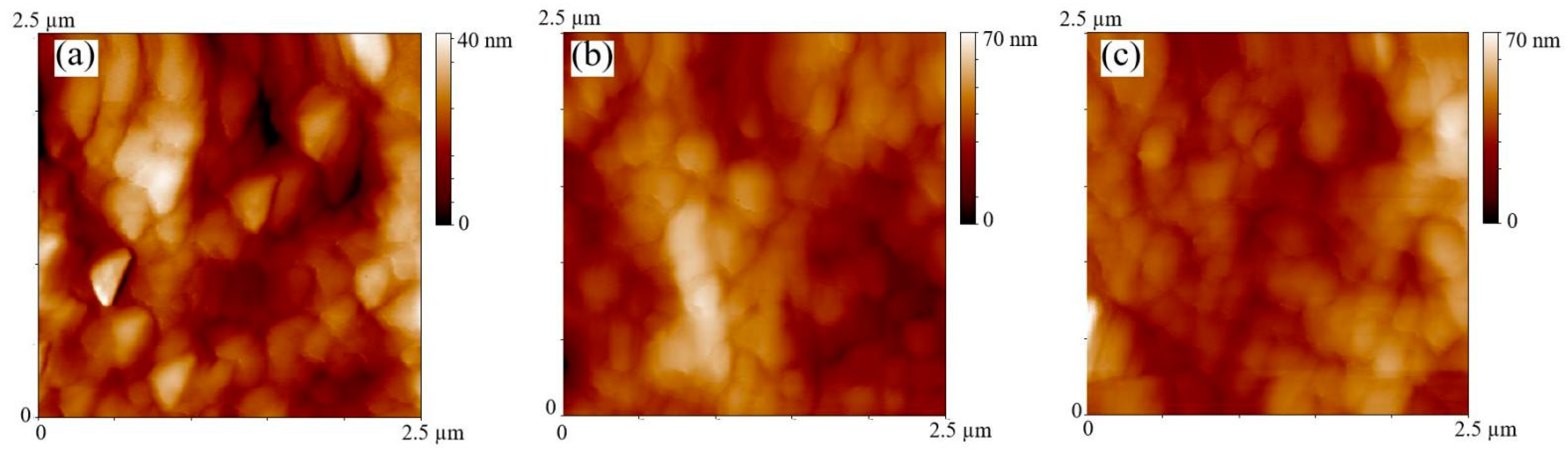
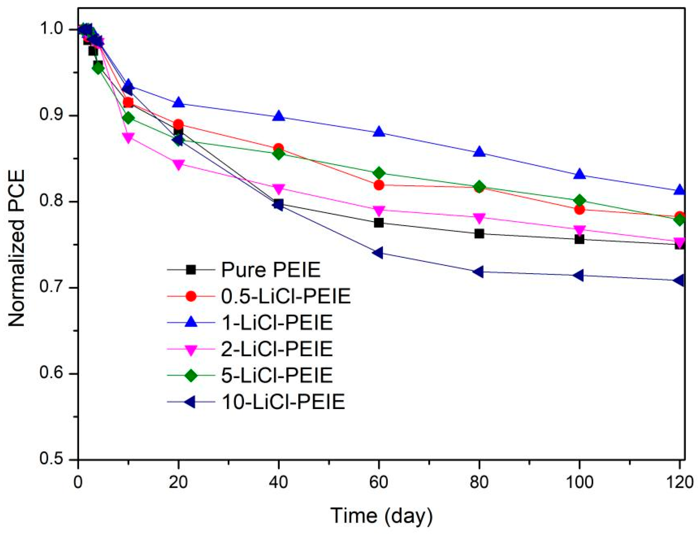
3. Results and Discussion
4. Conclusions
Author Contributions
Funding
Institutional Review Board Statement
Informed Consent Statement
Data Availability Statement
Conflicts of Interest
References
- Lu, B.S.; Zhang, Y.M.; Hu, T.Y.; Ma, Y.F.; Zhu, Y.N.; Liu, D.W.; Zhang, Z.Q.; Wang, E.H.; Ma, W.; Zhang, H.L. Non-fullerene acceptors based on multiple non-covalent interactions for low cost and air stable organic solar cells. Org. Electron. 2021, 93, 106132. [Google Scholar] [CrossRef]
- Yu, J.S.; Xi, Y.Y.; Chueh, C.C.; Xu, J.; Zhong, H.L.; Lin, F.; Jo, S.B.; Pozzo, L.D.; Tang, W.H.; Jen, A.K.-Y. Boosting performance of inverted organic solar cells by using a planar coronene based electron-transporting layer. Nano Energy 2017, 39, 454–460. [Google Scholar] [CrossRef]
- Duan, L.P.; Ashraf, U. Progress in stability of organic solar cells. Adv. Sci. 2020, 39, 1903259. [Google Scholar] [CrossRef] [Green Version]
- Jeong, M.; Ho, C.J.; Lee, J.H.; Moon, D.K.; Kim, J.H. Effect of interface modification in polymer solar cells: An in-depth investigation of the structural variation of organic dye for interlayer material. Dyes Pigm. 2020, 173, 107927. [Google Scholar] [CrossRef]
- Wang, C.H.; Yang, J.L. Interface modification for organic and perovskite solar cells. Sci. China Mater. 2016, 59, 743–756. [Google Scholar] [CrossRef] [Green Version]
- Bi, S.Q.; Leng, X.Y.; Li, Y.X.; Zheng, Z.; Zhang, X.N.; Zhang, Y.; Zhou, H.Q. Interfacial modification in organic and perovskite solar cells. Adv. Mater. 2019, 31, 1805708. [Google Scholar] [CrossRef]
- Arbab, E.A.A.; Mola, G.T. Metals decorated nanocomposite assisted charge transport in polymer solar cell. Mater. Sci. Semicon. Proc. 2019, 91, 1–8. [Google Scholar] [CrossRef]
- Lin, Y.B.; Adilbekova, B.; Firdaus, Y.; Yengel, E.; Faber, H.; Sajjad, M.; Zheng, X.P.; Yarali, E.; Seitkhan, A.; Bakr, O.M.; et al. 17% efficient organic solar cells based on liquid exfoliated WS2 as a replacement for PEDOT:PSS. Adv. Mater. 2019, 31, 1902965. [Google Scholar] [CrossRef] [PubMed]
- Duan, L.P.; Sang, B.R.; He, M.R.; Zhang, Y.; Hossain, M.A.; Rahaman, M.H.; Wei, Q.Y.; Zou, Y.P.; Uddin, A.; Hoex, B. Interface modification enabled by atomic layer deposited ultra-thin titanium oxide for high-efficiency and semitransparent organic solar cells. Sol. RRL 2020, 4, 2000497. [Google Scholar] [CrossRef]
- Wang, D.F.; Tao, H.Z.; Zhao, X.J.; Zhang, T.J.; Han, J.B. TiO₂/P3HT hybrid solar cell with efficient interface modification by organic and inorganic materials: A comparative study. J. Nanosci Nanotechnol. 2016, 16, 797–801. [Google Scholar] [CrossRef] [PubMed]
- Khorshidi, E.; Rezaei, B.; Irannejad, N.; Adhami, S.; Ebrahimi, M.; Kermanpur, A.; Ensafi, A.A. The role of GQDs additive in TiO2 nanorods as an electron transfer layer on performance improvement of the perovskite solar cells. Electrochim. Acta. 2020, 337, 135822. [Google Scholar] [CrossRef]
- Huang, S.H.; Ali, N.; Huai, Z.X.; Ren, J.P.; Sun, Y.S.; Zhao, X.H.; Fu, G.S.; Kong, W.G.; Yang, S.P. A facile strategy for enhanced performance of inverted organic solar cells based on low-temperature solution-processed SnO2 electron transport layer. Org. Electron. 2020, 78, 105555. [Google Scholar] [CrossRef]
- Liu, B.C.; Lan, L.H.; Liu, Y.Y.; Tao, H.; Li, H.M.; Xu, H.; Zou, J.H.; Xu, M.; Wang, L.; Peng, J.B.; et al. Improved performance of quantum dot light-emitting diodes by hybrid electron transport layer comprised of ZnO nanoparticles doped organic small molecule. Org. Electron. 2019, 74, 144–151. [Google Scholar] [CrossRef]
- Peng, L.P.; Liu, Z.T. Reduce the hysteresis effect with the PEIE interface dipole effect in the organic-inorganic hybrid perovskite CH3NH3PbI3-Xclx solar cell. Org. Electron. 2018, 62, 630–636. [Google Scholar] [CrossRef]
- Yu, H.Z.; Huang, X.X.; Huang, C.W. PEIE doped ZnO as a tunable cathode interlayer for efficient polymer solar cells. Appl. Surf. Sci. 2019, 470, 318–330. [Google Scholar] [CrossRef]
- Kim, J.; Lee, H.; Lee, S.J.; Silva, W.J.; Yusoff, A.R.B.M.; Jang, J. Graphene oxide grafted polyethylenimine electron transport material for highly efficient organic devices. J. Mater. Chem. A 2015, 3, 22035–22042. [Google Scholar] [CrossRef]
- Ling, Z.T.; Zhao, Y.; Wang, S.L.; Pan, S.H.; Lian, H.; Peng, C.Y.; Yang, X.Y.; Liao, Y.J.; Lan, W.X.; Wei, B.; et al. High-performance light-soaking-free polymer solar cells based on a lif modified ZnO electron extraction layer. J. Mater. Chem. C 2019, 7, 9354–9361. [Google Scholar] [CrossRef]
- Huang, Y.Y.; Li, S.N.; Wu, C.R.; Wang, S.; Wang, C.Y.; Ma, R.X. Introduction of Licl into SnO2 electron transport layer for efficient planar perovskite solar cells. Chem. Phys. Lett. 2020, 745, 137220. [Google Scholar] [CrossRef]
- Sheng, Y.S.; Hu, Y.; Mei, A.Y.; Jiang, P.; Hou, X.M.; Duan, M.; Hong, L.; Guan, Y.J.; Rong, Y.G.; Xiong, Y.L.; et al. Enhanced electronic properties in CH3NH3PbI3 via LiCl mixing for hole-conductor-free printable perovskite solar cells. J. Mater. Chem. A 2016, 4, 16731–16736. [Google Scholar] [CrossRef]
- Yin, S.M.; Yuan, Y.F.; Guo, S.Y.; Ren, Z.H.; Han, G.R. Li+ Ion induced three-dimensional aggregation growth of single-crystal perovskite octahedrons. Cryst. Eng. Comm. 2016, 18, 7849–7854. [Google Scholar] [CrossRef]
- Yin, S.M.; Tian, H.; Ren, Z.H.; Wei, X.; Chao, C.Y.; Pei, J.Y.; Li, X.; Xu, G.; Shen, G.; Han, G.R. Octahedral-shaped perovskite nanocrystals and their visible-light photocatalytic activity. Chem. Commun. 2014, 50, 6027–6030. [Google Scholar] [CrossRef]
- Lee, H.W.; Oh, J.Y.; Lee, T.I.; Jang, W.S.; Yoo, Y.B.; Chae, S.S.; Park, J.H.; Myoung, J.M.; Song, K.M.; Baik, H.K. Highly efficient inverted polymer solar cells with reduced graphene-oxide–zinc-oxide nanocomposites buffer layer. Appl. Phys. Lett. 2013, 102, 193903. [Google Scholar] [CrossRef]
- Li, P.; Jiang, Z.Z.; Huang, H.S.; Tian, S.J.; Hu, X.Y.; Li, W.J.; Bao, X.; Wang, Y. Improving electron transport by using a NaCl/Polyethylenimine ethoxylated double layer for high-efficiency polymer solar cells. Mat. Sci. Semicon. Proc. 2020, 116, 105150. [Google Scholar] [CrossRef]
- Sirringhaus, H.; Brown, P.J.; Friend, R.H.; Nielsen, M.M.; Bechgaard, K.; Langeveld-Voss, B.M.W.; Spiering, A.J.H.; Janssen, R.A.J.; Meijer, E.W.; Herwig, P.; et al. Two-dimensional charge transport in self-organized, highmobility conjugated polymers. Nature 1999, 401, 685–688. [Google Scholar] [CrossRef]
- Uddin, M.A.; Lee, T.H.; Xu, S.H.; Park, S.Y.; Kim, T.; Song, S.; Nguyen, T.L.; Ko, S.J.; Hwang, S.; Kim, J.Y.; et al. Interplay of intramolecular noncovalent coulomb interactions for semicrystalline photovoltaic polymers. Chem. Mater. 2015, 27, 5997–6007. [Google Scholar] [CrossRef]
- Cho, K.; Kim, J.; Yoon, S.Y.; Ryu, K.Y.; Jang, S.R.; Lim, B.; Kim, K. Reducing trap-assisted recombination in small organic molecule-based photovoltaics by the addition of a conjugated block copolymer. Macromol. Rapid Commun. 2017, 39, 1700630. [Google Scholar] [CrossRef] [PubMed]
- Ghazy, O.A. Water-based blend nanoparticles of P3HT and PCBM for the application in organic solar cells. Adv. Polym. Technol. 2015, 34, 21500. [Google Scholar] [CrossRef]
- Wang, Z.X.; Zhang, F.J.; Wang, J.; Xu, X.W.; Wang, J.; Liu, Y.; Xu, Z. Organic photovoltaic cells: Novel organic semiconducting materials and molecular arrangement engineering. Chin. Sci. Bull. 2012, 57, 4143–4152. [Google Scholar] [CrossRef] [Green Version]
- You, D.S.; Kim, C.S.; Kang, Y.J.; Lim, K.; Jung, S.; Kim, D.G.; Kim, J.K.; Jo, S.J.; Kim, J.H.; Kang, J.W. Annealing-free poly(3-Hexylthiophene):[6,6]-Phenyl-C61-butyric acid methyl ester-based organic solar cells. Curr. Appl. Phys. 2012, 12, 908–910. [Google Scholar] [CrossRef]


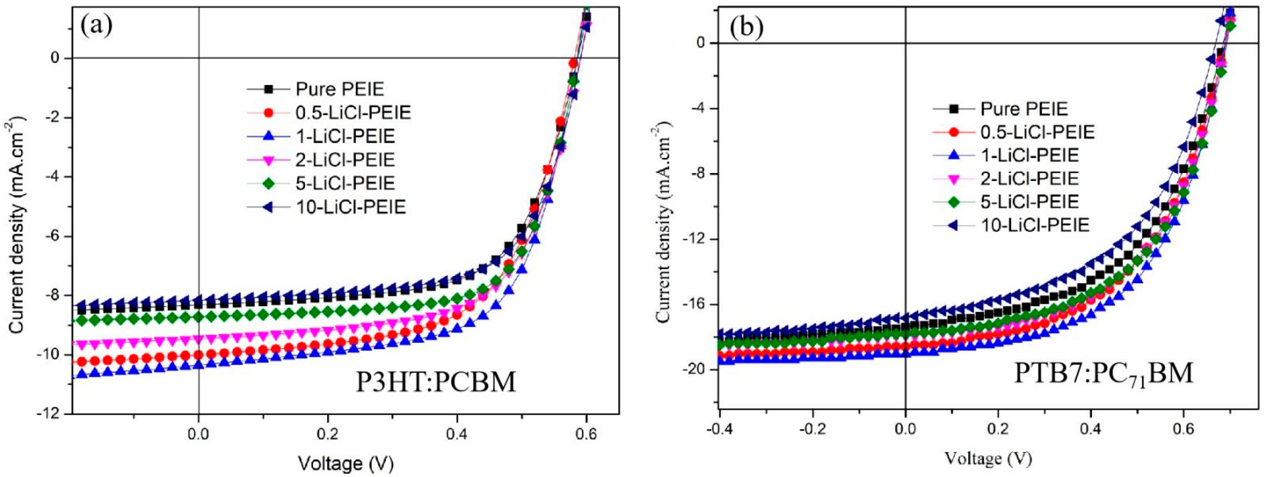
| Device | Vo (V) | Jsc (mA·cm−2) | FF (%) | Rs (Ω·cm2) | Rsh (Ω·cm2) | PCE (%) | |
|---|---|---|---|---|---|---|---|
| Highest | Average a | ||||||
| Pure PEIE | 0.58 | 8.32 | 65.5 | 11.3 | 1281 | 3.16 | 3.04 |
| 0.5-LiC-PEIE | 0.58 | 10.01 | 60.1 | 9.6 | 1832 | 3.54 | 3.43 |
| 1-LiCl-PEIE | 0.58 | 10.36 | 62.8 | 7.5 | 1982 | 3.84 | 3.61 |
| 2-LiCl-PEIE | 0.58 | 9.44 | 64.4 | 9.9 | 1652 | 3.53 | 3.21 |
| 5-LiCl-PEIE | 0.58 | 8.72 | 68.2 | 11.7 | 1127 | 3.45 | 3.19 |
| 10-LiCl-PEIE | 0.59 | 8.16 | 66.0 | 15.1 | 987 | 3.12 | 2.98 |
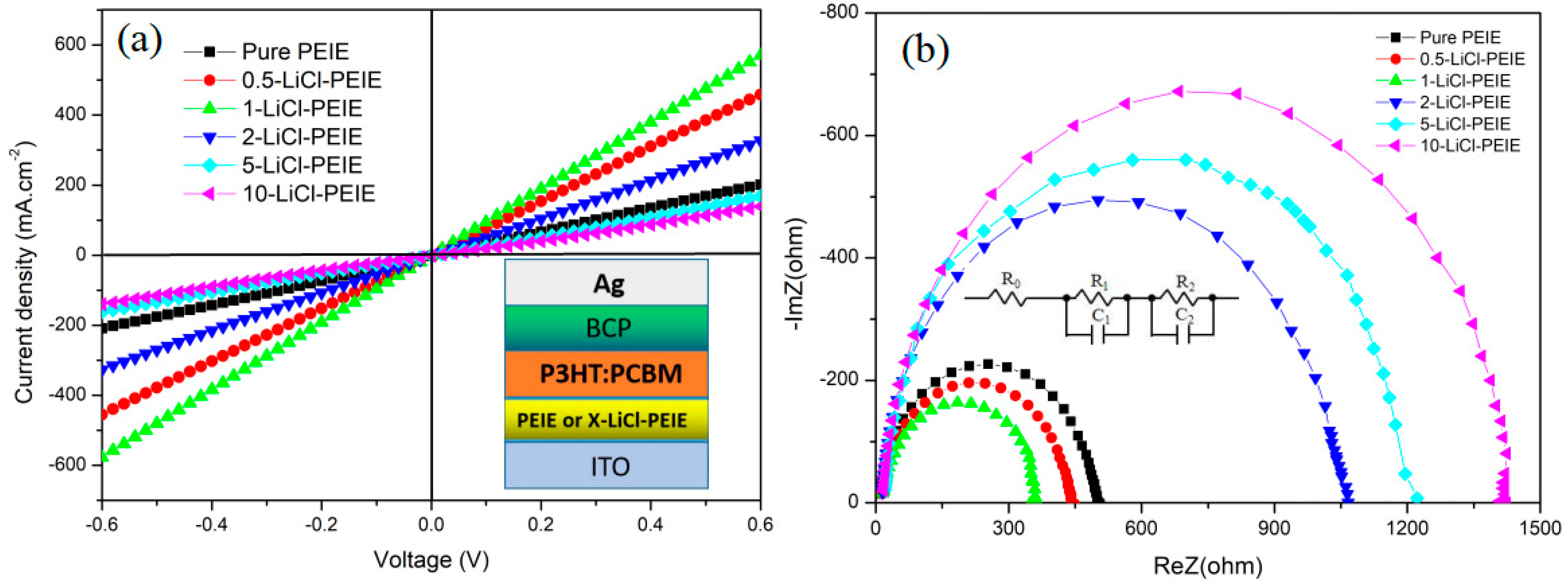
| Device | R0 (Ω) | R1 (Ω) | R2 (Ω) |
|---|---|---|---|
| Pure PEIE | 85.23 | 79.15 | 332.12 |
| 0.5-LiC-PEIE | 73.14 | 68.51 | 285.54 |
| 1-LiCl-PEIE | 62.42 | 50.78 | 170.17 |
| 2-LiCl-PEIE | 130.73 | 127.61 | 433.16 |
| 5-LiCl-PEIE | 178.81 | 153.52 | 489.22 |
| 10-LiCl-PEIE | 245.95 | 331.19 | 888.25 |
Publisher’s Note: MDPI stays neutral with regard to jurisdictional claims in published maps and institutional affiliations. |
© 2021 by the authors. Licensee MDPI, Basel, Switzerland. This article is an open access article distributed under the terms and conditions of the Creative Commons Attribution (CC BY) license (https://creativecommons.org/licenses/by/4.0/).
Share and Cite
Li, P.; Chen, L.; Hu, X.; He, L.; Jiang, Z.; Luo, M.; Huang, H.; Yuan, W.; He, Y. Effective Double Electron Transport Layer Inducing Crystallization of Active Layer for Improving the Performance of Organic Solar Cells. Nanomaterials 2022, 12, 15. https://0-doi-org.brum.beds.ac.uk/10.3390/nano12010015
Li P, Chen L, Hu X, He L, Jiang Z, Luo M, Huang H, Yuan W, He Y. Effective Double Electron Transport Layer Inducing Crystallization of Active Layer for Improving the Performance of Organic Solar Cells. Nanomaterials. 2022; 12(1):15. https://0-doi-org.brum.beds.ac.uk/10.3390/nano12010015
Chicago/Turabian StyleLi, Ping, Lijia Chen, Xiaoyan Hu, Lirong He, Zezhuan Jiang, Minghao Luo, Haishen Huang, Wei Yuan, and Yinghu He. 2022. "Effective Double Electron Transport Layer Inducing Crystallization of Active Layer for Improving the Performance of Organic Solar Cells" Nanomaterials 12, no. 1: 15. https://0-doi-org.brum.beds.ac.uk/10.3390/nano12010015