
A Morphological Study of Solvothermally Grown SnO2 Nanostructures for Application in Perovskite Solar Cells

 , , ,
, , ,  and
and 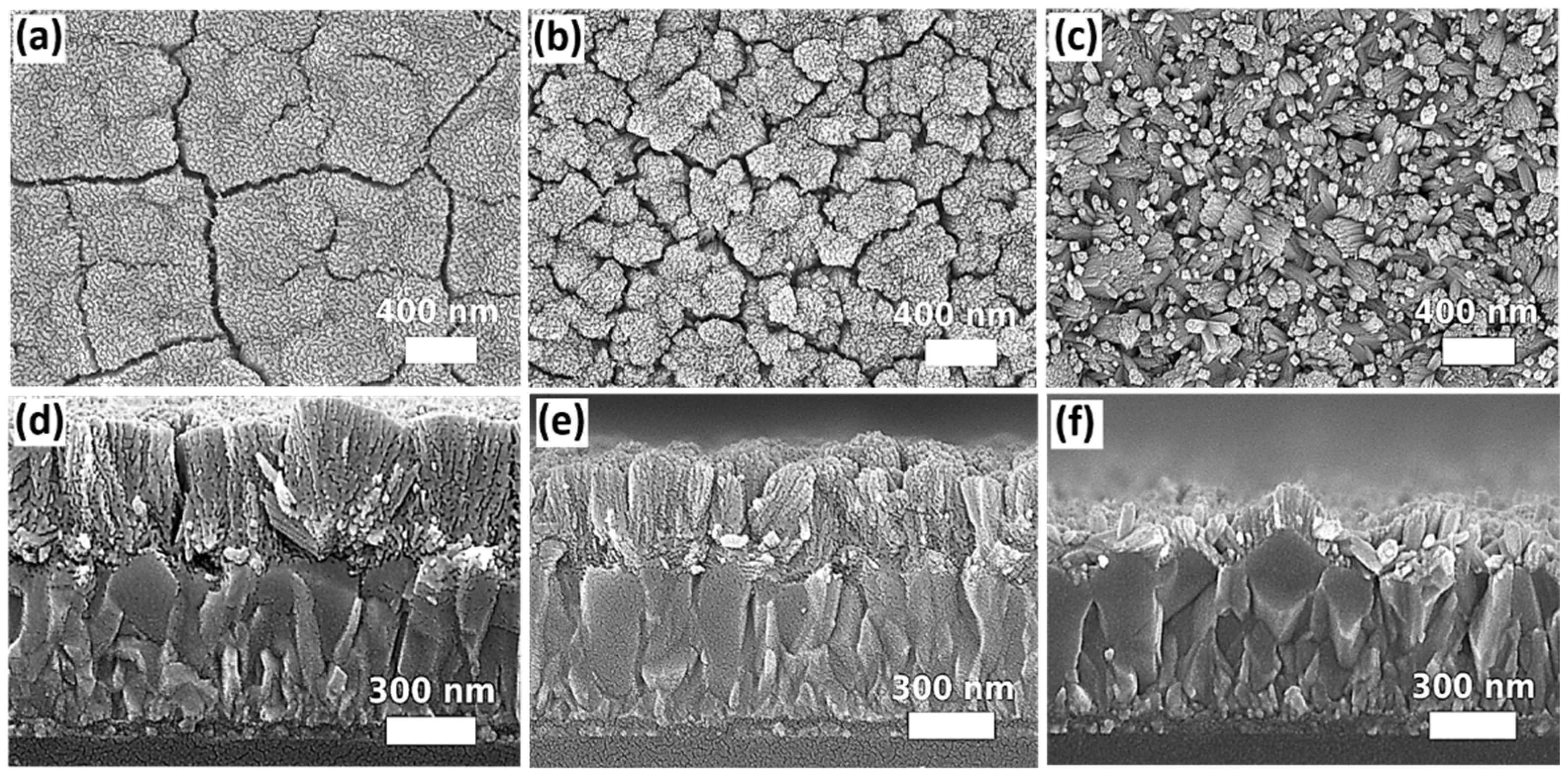
Abstract
:1. Introduction
2. Experimental Details
2.1. Synthesis of SnO2 Nanorod Arrays
2.2. Preparation of SnO2 Nanorod Arrays Using Different Growth Parameters
2.2.1. Growth Pressure
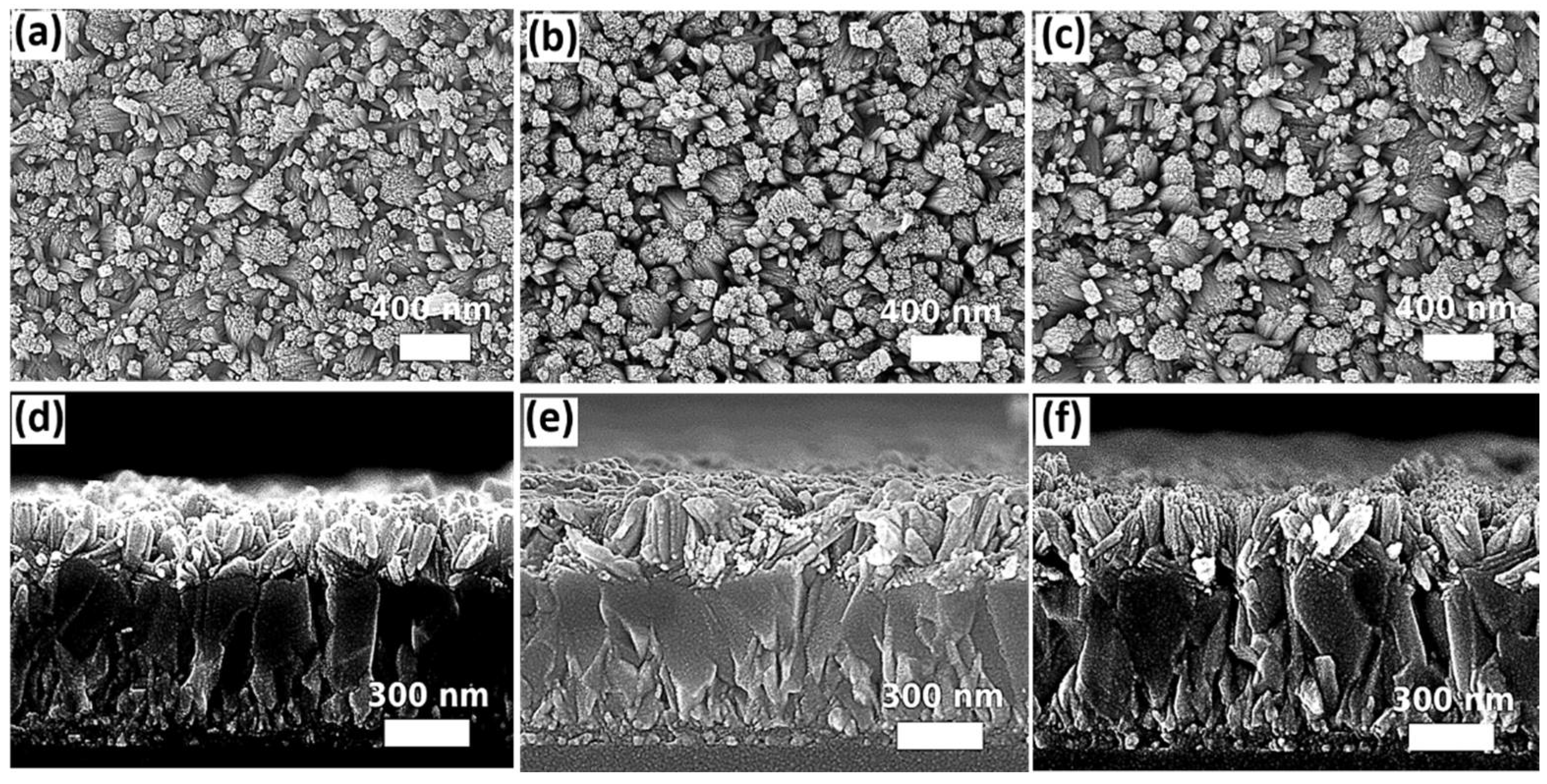
2.2.2. Substrate Orientation
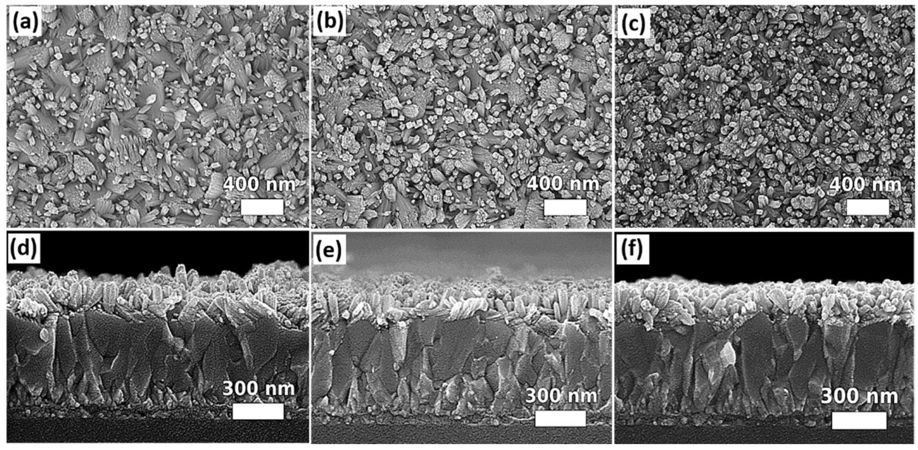
2.2.3. DI Water-to-Ethanol Ratios
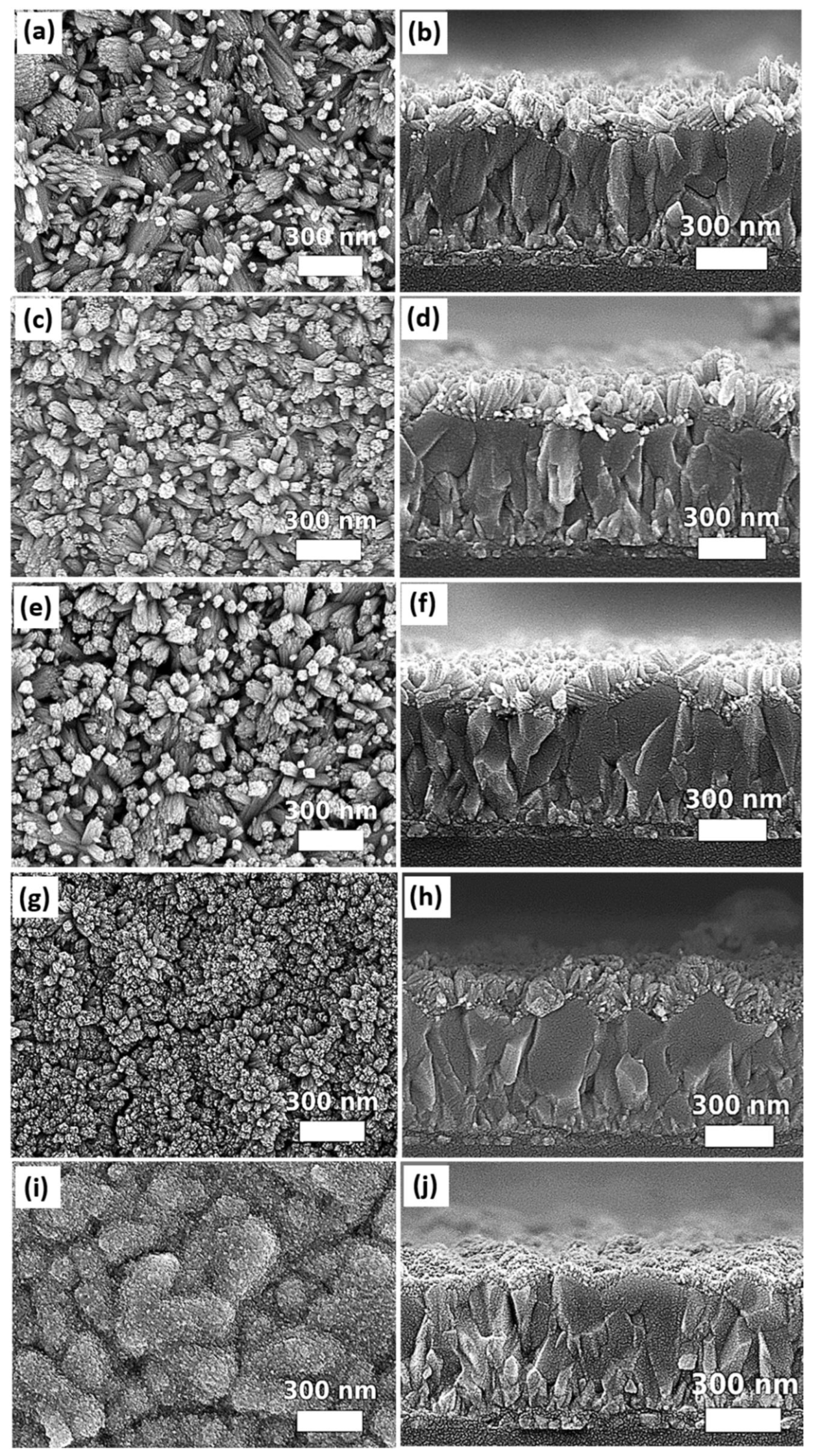
2.2.4. Seed Layers
2.2.5. Glacial Acetic Acid
2.2.6. Growth Time
2.3. The Perovskite Solution
3. Results and Discussions
4. Conclusions
Supplementary Materials
Author Contributions
Funding
Institutional Review Board Statement
Informed Consent Statement
Data Availability Statement
Acknowledgments
Conflicts of Interest
References
- Jeong, J.; Kim, M.; Seo, J.; Lu, H.; Ahlawat, P.; Mishra, A.; Yang, Y.; Hope, M.A.; Eickemeyer, F.T.; Kim, M.; et al. Pseudo-halide anion engineering for α-FAPbI3 perovskite solar cells. Nature 2021, 592, 381–385. [Google Scholar] [CrossRef] [PubMed]
- Roy, P.; Kumar Sinha, N.; Tiwari, S.; Khare, A. A review on perovskite solar cells: Evolution of architecture, fabrication tech-niques, commercialization issues and status. Sol. Energy 2020, 198, 665–688. [Google Scholar] [CrossRef]
- Djurišić, A.B.; Liu, F.Z.; Tam, H.W.; Wong, M.K.; Ng, A.; Surya, C.; Chen, W.; He, Z.B. Perovskite solar cells—An overview of critical issues. Prog. Quantum Electron. 2017, 53, 1–37. [Google Scholar] [CrossRef]
- Olzhabay, Y.; Ng, A.; Ukaegbu, I.A. Perovskite PV energy harvesting system for uninterrupted IoT device applications. Energies 2021, 14, 7946. [Google Scholar] [CrossRef]
- Djurišić, A.B.; Liu, F.; Ng, A.M.C.; Dong, Q.; Wong, M.K.; Ng, A.; Surya, C. Stability issues of the next generation solar cells. Physica Status Solidi (RRL)—Rapid Res. Lett. 2016, 10, 281–299. [Google Scholar] [CrossRef]
- Li, Z.; Klein, T.R.; Kim, D.H.; Yang, M.; Berry, J.J.; van Hest, M.F.A.M.; Zhu, K. Scalable fabrication of perovskite solar cells. Nat. Rev. Mater. 2018, 3, 18017. [Google Scholar] [CrossRef]
- Wong, M.K.; Liu, F.; Kam, C.S.; Leung, T.L.; Tam, H.W.; Djurišić, A.B.; Popović, J.; Li, H.; Shih, K.; Low, K.-H.; et al. Synthesis of Lead-Free Perovskite Films by Combinatorial Evaporation: Fast Processes for Screening Different Precursor Combinations. Chem. Mater. 2017, 29, 9946–9953. [Google Scholar] [CrossRef]
- Lu, H.; Krishna, A.; Zakeeruddin, S.M.; Grätzel, M.; Hagfeldt, A. Compositional and Interface Engineering of Organ-ic-Inorganic Lead Halide Perovskite Solar Cells. iScience 2020, 23, 101359. [Google Scholar] [CrossRef]
- Gedamu, D.; Asuo, I.M.; Benetti, D.; Basti, M.; Ka, I.; Cloutier, S.G.; Rosei, F.; Nechache, R. Solvent-Antisolvent Ambient Processed Large Grain Size Perovskite Thin Films for High-Performance Solar Cells. Sci. Rep. 2018, 8, 12885. [Google Scholar] [CrossRef]
- Ng, A.; Ren, Z.; Hu, H.; Fong, P.W.K.; Shen, Q.; Cheung, S.H.; Qin, P.; Lee, J.-W.; Djurišić, A.B.; So, S.K.; et al. A Cryogenic Process for Antisolvent-Free High-Performance Perovskite Solar Cells. Adv. Mater. 2018, 30, 1804402. [Google Scholar] [CrossRef]
- Aydin, E.; De Bastiani, M.; De Wolf, S. Defect and Contact Passivation for Perovskite Solar Cells. Adv. Mater. 2019, 31, 1900428. [Google Scholar] [CrossRef] [PubMed]
- Aidarkhanov, D.; Ren, Z.; Lim, C.-K.; Yelzhanova, Z.; Nigmetova, G.; Taltanova, G.; Baptayev, B.; Liu, F.; Cheung, S.H.; Balanay, M.; et al. Passivation engineering for hysteresis-free mixed perovskite solar cells. Sol. Energy Mater. Sol. Cells 2020, 215, 110648. [Google Scholar] [CrossRef]
- Ren, Z.; Zhou, J.; Zhang, Y.; Ng, A.; Shen, Q.; Cheung, S.H.; Shen, H.; Li, K.; Zheng, Z.; So, S.K.; et al. Strategies for high performance perovskite/crystalline silicon four-terminal tandem solar cells. Sol. Energy Mater. Sol. Cells 2018, 179, 36–44. [Google Scholar] [CrossRef]
- Peng, J.; Duong, T.; Zhou, X.; Shen, H.; Wu, Y.; Mulmudi, H.K.; Wan, Y.; Zhong, D.; Li, J.; Tsuzuki, T.; et al. Efficient Indi-um-Doped TiOx Electron Transport Layers for High-Performance Perovskite Solar Cells and Perovskite-Silicon Tandems. Adv. Energy Mater. 2017, 7, 1601768. [Google Scholar] [CrossRef] [Green Version]
- Abdi-Jalebi, M.; Dar, M.I.; Sadhanala, A.; Senanayak, S.P.; Giordano, F.; Zakeeruddin, S.M.; Grätzel, M.; Friend, R.H. Impact of a Mesoporous Titania–Perovskite Interface on the Performance of Hybrid Organic–Inorganic Perovskite Solar Cells. J. Phys. Chem. Lett. 2016, 7, 3264–3269. [Google Scholar] [CrossRef] [Green Version]
- Huang, F.; Pascoe, A.R.; Wu, W.-Q.; Ku, Z.; Peng, Y.; Zhong, J.; Caruso, R.A.; Cheng, Y.-B. Effect of the Microstructure of the Functional Layers on the Efficiency of Perovskite Solar Cells. Adv. Mater. 2017, 29, 1601715. [Google Scholar] [CrossRef]
- Vasilopoulou, M.; Georgiadou, D.G.; Soultati, A.; Boukos, N.; Gardelis, S.; Palilis, L.C.; Fakis, M.; Skoulatakis, G.; Kennou, S.; Botzakaki, M.; et al. Atomic-Layer-Deposited Aluminum and Zirconium Oxides for Surface Passivation of TiO2 in High-Efficiency Organic Photovoltaics. Adv. Energy Mater. 2014, 4, 1400214. [Google Scholar] [CrossRef]
- Wu, Z.; Yu, H.; Shi, S.; Li, Y. Bismuth oxysulfide modified ZnO nanorod arrays as an efficient electron transport layer for inverted polymer solar cells. J. Mater. Chem. A 2019, 7, 14776–14789. [Google Scholar] [CrossRef]
- Vasilopoulou, M. The effect of surface hydrogenation of metal oxides on the nanomorphology and the charge generation effi-ciency of polymer blend solar cells. Nanoscale 2014, 6, 13726–13739. [Google Scholar] [CrossRef]
- Mingorance, A.; Xie, H.; Kim, H.-S.; Wang, Z.; Balsells, M.; Morales-Melgares, A.; Domingo, N.; Kazuteru, N.; Tress, W.; Fraxedas, J.; et al. Interfacial Engineering of Metal Oxides for Highly Stable Halide Perovskite Solar Cells. Adv. Mater. Interfaces 2018, 5, 1800367. [Google Scholar] [CrossRef]
- Zhou, Y.; Li, X.; Lin, H. To Be Higher and Stronger—Metal Oxide Electron Transport Materials for Perovskite Solar Cells. Small 2020, 16, 1902579. [Google Scholar] [CrossRef] [PubMed]
- Shin, S.S.; Lee, S.J.; Seok, S.I. Metal Oxide Charge Transport Layers for Efficient and Stable Perovskite Solar Cells. Adv. Funct. Mater. 2019, 29, 1900455. [Google Scholar] [CrossRef]
- Mahmood, K.; Sarwar, S.; Mehran, M.T. Current status of electron transport layers in perovskite solar cells: Materials and properties. RSC Adv. 2017, 7, 17044–17062. [Google Scholar] [CrossRef] [Green Version]
- Liu, C.; Zhu, R.; Ng, A.; Ren, Z.; Cheung, S.H.; Du, L.; So, S.K.; Zapien, J.A.; Djurišić, A.B.; Lee Phillips, D.; et al. Investigation of high performance TiO2 nanorod array perovskite solar cells. J. Mater. Chem. A 2017, 5, 15970–15980. [Google Scholar] [CrossRef]
- Cao, B.; Liu, H.; Yang, L.; Li, X.; Liu, H.; Dong, P.; Mai, X.; Hou, C.; Wang, N.; Zhang, J.; et al. Interfacial Engineering for High-Efficiency Nanorod Array-Structured Perovskite Solar Cells. ACS Appl. Mater. Interfaces 2019, 11, 33770–33780. [Google Scholar] [CrossRef] [PubMed]
- Li, X.; Dai, S.-M.; Zhu, P.; Deng, L.-L.; Xie, S.-Y.; Cui, Q.; Chen, H.; Wang, N.; Lin, H. Efficient Perovskite Solar Cells Depending on TiO2 Nanorod Arrays. ACS Appl. Mater. Interfaces 2016, 8, 21358–21365. [Google Scholar] [CrossRef]
- Manseki, K.; Ikeya, T.; Tamura, A.; Ban, T.; Sugiura, T.; Yoshida, T. Mg-doped TiO2 nanorods improving open-circuit voltages of ammonium lead halide perovskite solar cells. RSC Adv. 2014, 4, 9652–9655. [Google Scholar] [CrossRef]
- Yang, L.; Wang, X.; Mai, X.; Wang, T.; Wang, C.; Li, X.; Murugadoss, V.; Shao, Q.; Angaiah, S.; Guo, Z. Constructing efficient mixed-ion perovskite solar cells based on TiO2 nanorod array. J. Colloid Interface Sci. 2019, 534, 459–468. [Google Scholar] [CrossRef]
- Li, Y.; Guo, Y.; Li, Y.; Zhou, X. Fabrication of Cd-Doped TiO2 Nanorod Arrays and Photovoltaic Property in Perovskite Solar Cell. Electrochim. Acta 2016, 200, 29–36. [Google Scholar] [CrossRef]
- Wu, S.; Chen, C.; Wang, J.; Xiao, J.; Peng, T. Controllable Preparation of Rutile TiO2 Nanorod Array for Enhanced Photovoltaic Performance of Perovskite Solar Cells. ACS Appl. Energy Mater. 2018, 1, 1649–1657. [Google Scholar] [CrossRef]
- Cui, Q.; Zhao, X.; Lin, H.; Yang, L.; Chen, H.; Zhang, Y.; Li, X. Improved efficient perovskite solar cells based on Ta-doped TiO2 nanorod arrays. Nanoscale 2017, 9, 18897–18907. [Google Scholar] [CrossRef] [PubMed]
- Lv, Y.; Li, Y.; Sun, H.; Guo, Y.; Li, Y.; Tan, J.; Zhou, X. Yttrium-doped TiO2 nanorod arrays and application in perovskite solar cells for enhanced photocurrent density. Thin Solid Film. 2018, 651, 117–123. [Google Scholar] [CrossRef]
- Xiao, G.; Shi, C.; Lv, K.; Ying, C.; Wang, Y. Nb-Doping TiO2 Electron Transporting Layer for Efficient Perovskite Solar Cells. ACS Appl. Energy Mater. 2018, 1, 2576–2581. [Google Scholar] [CrossRef]
- Yang, M.; Guo, R.; Kadel, K.; Liu, Y.; O’Shea, K.; Bone, R.; Wang, X.; He, J.; Li, W. Improved charge transport of Nb-doped TiO2 nanorods in methylammonium lead iodide bromide perovskite solar cells. J. Mater. Chem. A 2014, 2, 19616–19622. [Google Scholar] [CrossRef]
- Yu, Y.; Li, J.; Geng, D.; Wang, J.; Zhang, L.; Andrew, T.L.; Arnold, M.S.; Wang, X. Development of Lead Iodide Perovskite Solar Cells Using Three-Dimensional Titanium Dioxide Nanowire Architectures. ACS Nano 2015, 9, 564–572. [Google Scholar] [CrossRef] [PubMed]
- Tao, H.; Ke, W.; Wang, J.; Liu, Q.; Wan, J.; Yang, G.; Fang, G. Perovskite solar cell based on network nanoporous layer consisted of TiO2 nanowires and its interface optimization. J. Power Sources 2015, 290, 144–152. [Google Scholar] [CrossRef]
- Wu, W.-Q.; Chen, D.; Cheng, Y.-B.; Caruso, R.A. Low-Temperature Solution-Processed Amorphous Titania Nanowire Thin Films for 1 cm2 Perovskite Solar Cells. ACS Appl. Mater. Interfaces 2020, 12, 11450–11458. [Google Scholar] [CrossRef]
- Wu, W.-Q.; Huang, F.; Chen, D.; Cheng, Y.-B.; Caruso, R.A. Thin Films of Dendritic Anatase Titania Nanowires Enable Ef-fective Hole-Blocking and Efficient Light-Harvesting for High-Performance Mesoscopic Perovskite Solar Cells. Adv. Funct. Mater. 2015, 25, 3264–3272. [Google Scholar] [CrossRef]
- Elseman, A.M.; Zaki, A.H.; Shalan, A.E.; Rashad, M.M.; Song, Q.L. TiO2 Nanotubes: An Advanced Electron Transport Material for Enhancing the Efficiency and Stability of Perovskite Solar Cells. Ind. Eng. Chem. Res. 2020, 59, 18549–18557. [Google Scholar] [CrossRef]
- Wu, S.; Cheng, C.; Jin, J.; Wang, J.; Peng, T. Low-Temperature Processed Nanostructured Rutile TiO2 Array Films for Perovskite Solar Cells with High Efficiency and Stability. Sol. RRL 2018, 2, 1700164. [Google Scholar] [CrossRef]
- Mali, S.S.; Shim, C.S.; Kim, H.; Betty, C.A.; Patil, P.S.; Hong, C.K. Secondary Hydrothermally Processed Engineered Titanium Dioxide Nanostructures for Efficient Perovskite Solar Cells. Energy Technol. 2017, 5, 1775–1787. [Google Scholar] [CrossRef] [Green Version]
- Zhang, R.; Fei, C.; Li, B.; Fu, H.; Tian, J.; Cao, G. Continuous Size Tuning of Monodispersed ZnO Nanoparticles and Its Size Effect on the Performance of Perovskite Solar Cells. ACS Appl. Mater. Interfaces 2017, 9, 9785–9794. [Google Scholar] [CrossRef] [PubMed]
- Li, S.; Zhang, P.; Wang, Y.; Sarvari, H.; Liu, D.; Wu, J.; Yang, Y.; Wang, Z.; Chen, Z.D. Interface engineering of high efficiency perovskite solar cells based on ZnO nanorods using atomic layer deposition. Nano Res. 2017, 10, 1092–1103. [Google Scholar] [CrossRef]
- Liang, L.; Huang, Z.; Cai, L.; Chen, W.; Wang, B.; Chen, K.; Bai, H.; Tian, Q.; Fan, B. Magnetron Sputtered Zinc Oxide Na-norods as Thickness-Insensitive Cathode Interlayer for Perovskite Planar-Heterojunction Solar Cells. ACS Appl. Mater. Interfaces 2014, 6, 20585–20589. [Google Scholar] [CrossRef]
- Mahmood, K.; Swain, B.S.; Amassian, A. 16.1% Efficient Hysteresis-Free Mesostructured Perovskite Solar Cells Based on Synergistically Improved ZnO Nanorod Arrays. Adv. Energy Mater. 2015, 5, 1500568. [Google Scholar] [CrossRef]
- Pelicano, C.M.; Yanagi, H. Efficient solid-state perovskite solar cells based on nanostructured zinc oxide designed by strategic low temperature water oxidation. J. Mater. Chem. C 2017, 5, 8059–8070. [Google Scholar] [CrossRef]
- Zhao, X.; Shen, H.; Sun, R.; Luo, Q.; Li, X.; Zhou, Y.; Tai, M.; Li, J.; Gao, Y.; Li, X.; et al. Bending Durable and Recyclable Mesostructured Perovskite Solar Cells Based on Superaligned ZnO Nanorod Electrode. Sol. RRL 2018, 2, 1700194. [Google Scholar] [CrossRef]
- Wang, H.; Yan, L.; Liu, J.; Li, J.; Wang, H. Fabrication of well-aligned ZnO nanorod photoanodes for perovskite solar cells. J. Mater. Sci. Mater. Electron. 2016, 27, 6872–6880. [Google Scholar] [CrossRef]
- Son, D.-Y.; Bae, K.-H.; Kim, H.-S.; Park, N.-G. Effects of Seed Layer on Growth of ZnO Nanorod and Performance of Perovskite Solar Cell. J. Phys. Chem. C 2015, 119, 10321–10328. [Google Scholar] [CrossRef]
- Chen, P.; Yin, X.; Que, M.; Yang, Y.; Que, W. TiO2 passivation for improved efficiency and stability of ZnO nanorods based perovskite solar cells. RSC Adv. 2016, 6, 57996–58002. [Google Scholar] [CrossRef]
- Garcia, V.J.; Pelicano, C.M.; Yanagi, H. Low temperature-processed ZnO nanorods-TiO2 nanoparticles composite as electron transporting layer for perovskite solar cells. Thin Solid Film. 2018, 662, 70–75. [Google Scholar] [CrossRef]
- Zhang, P.; Wu, J.; Zhang, T.; Wang, Y.; Liu, D.; Chen, H.; Ji, L.; Liu, C.; Ahmad, W.; Chen, Z.D.; et al. Perovskite Solar Cells with ZnO Electron-Transporting Materials. Adv. Mater. 2018, 30, 1703737. [Google Scholar] [CrossRef]
- Singh, M.; Chu, C.W.; Ng, A. Perspective on Predominant Metal Oxide Charge Transporting Materials for High-Performance Perovskite Solar Cells. Front. Mater. 2021, 8, 655207. [Google Scholar] [CrossRef]
- Zhang, D.-F.; Sun, L.-D.; Yin, J.-L.; Yan, C.-H. Low-Temperature Fabrication of Highly Crystalline SnO2 Nanorods. Adv. Mater. 2003, 15, 1022–1025. [Google Scholar] [CrossRef]
- Sun, H.; Deng, K.; Zhu, Y.; Liao, M.; Xiong, J.; Li, Y.; Li, L. A Novel Conductive Mesoporous Layer with a Dynamic Two-Step Deposition Strategy Boosts Efficiency of Perovskite Solar Cells to 20%. Adv. Mater. 2018, 30, 1801935. [Google Scholar] [CrossRef]
- Zhang, X.; Rui, Y.; Wang, Y.; Xu, J.; Wang, H.; Zhang, Q.; Müller-Buschbaum, P. SnO2 nanorod arrays with tailored area density as efficient electron transport layers for perovskite solar cells. J. Power Sources 2018, 402, 460–467. [Google Scholar] [CrossRef]
- Lv, Y.; Wang, P.; Cai, B.; Ma, Q.; Zheng, X.; Wu, Y.; Jiang, Q.; Liu, J.; Zhang, W.-H. Facile Fabrication of SnO2 Nanorod Arrays Films as Electron Transporting Layer for Perovskite Solar Cells. Sol. RRL 2018, 2, 1800133. [Google Scholar] [CrossRef]
- Yeom, E.J.; Shin, S.S.; Yang, W.S.; Lee, S.J.; Yin, W.; Kim, D.; Noh, J.H.; Ahn, T.K.; Seok, S.I. Controllable synthesis of single crystalline Sn-based oxides and their application in perovskite solar cells. J. Mater. Chem. A 2017, 5, 79–86. [Google Scholar] [CrossRef]
- Xu, X.; Xu, Z.; Tang, J.; Zhang, X.; Zhang, L.; Wu, J.; Lan, Z. High-performance planar perovskite solar cells based on low-temperature solution-processed well-crystalline SnO2 nanorods electron-transporting layers. Chem. Eng. J. 2018, 351, 391–398. [Google Scholar] [CrossRef]
- Song, J.; Li, G.; Wang, D.; Sun, W.; Wu, J.; Lan, Z. High-Efficiency Low-Temperature-Processed Mesoscopic Perovskite Solar Cells from SnO2 Nanorod Self-Assembled Microspheres. Sol. RRL 2020, 4, 1900558. [Google Scholar] [CrossRef]
- Han, G.S.; Chung, H.S.; Kim, D.H.; Kim, B.J.; Lee, J.-W.; Park, N.-G.; Cho, I.S.; Lee, J.-K.; Lee, S.; Jung, H.S. Epitaxial 1D electron transport layers for high-performance perovskite solar cells. Nanoscale 2015, 7, 15284–15290. [Google Scholar] [CrossRef] [PubMed]
- Gao, C.; Yuan, S.; Cao, B.; Yu, J. SnO2 nanotube arrays grown via an in situ template-etching strategy for effective and stable perovskite solar cells. Chem. Eng. J. 2017, 325, 378–385. [Google Scholar] [CrossRef]
- Liu, Q.; Qin, M.-C.; Ke, W.-J.; Zheng, X.-L.; Chen, Z.; Qin, P.-L.; Xiong, L.-B.; Lei, H.-W.; Wan, J.-W.; Wen, J.; et al. Enhanced Stability of Perovskite Solar Cells with Low-Temperature Hydrothermally Grown SnO2 Electron Transport Layers. Adv. Funct. Mater. 2016, 26, 6069–6075. [Google Scholar] [CrossRef]
- Chen, S.; Wang, M.; Ye, J.; Cai, J.; Ma, Y.; Zhou, H.; Qi, L. Kinetics-controlled growth of aligned mesocrystalline SnO2 nanorod arrays for lithium-ion batteries with superior rate performance. Nano Res. 2013, 6, 243–252. [Google Scholar] [CrossRef]
- Yazdani, F.; Edrissi, M. Effect of pressure on the size of magnetite nanoparticles in the coprecipitation synthesis. Mater. Sci. Eng. B 2010, 171, 86–89. [Google Scholar] [CrossRef]
- Li, B.; Bian, K.; Zhou, X.; Lu, P.; Liu, S.; Brener, I.; Sinclair, M.; Luk, T.; Schunk, H.; Alarid, L.; et al. Pressure compression of CdSe nanoparticles into luminescent nanowires. Sci. Adv. 2017, 3, e1602916. [Google Scholar] [CrossRef] [Green Version]
- Patil, G.E.; Kajale, D.D.; Gaikwad, V.B.; Jain, G.H. Preparation and characterization of SnO2 nanoparticles by hydrothermal route. Int. Nano Lett. 2012, 2, 17. [Google Scholar] [CrossRef] [Green Version]


Publisher’s Note: MDPI stays neutral with regard to jurisdictional claims in published maps and institutional affiliations. |
© 2022 by the authors. Licensee MDPI, Basel, Switzerland. This article is an open access article distributed under the terms and conditions of the Creative Commons Attribution (CC BY) license (https://creativecommons.org/licenses/by/4.0/).
Share and Cite
Yelzhanova, Z.; Nigmetova, G.; Aidarkhanov, D.; Daniyar, B.; Baptayev, B.; Balanay, M.P.; Jumabekov, A.N.; Ng, A. A Morphological Study of Solvothermally Grown SnO2 Nanostructures for Application in Perovskite Solar Cells. Nanomaterials 2022, 12, 1686. https://0-doi-org.brum.beds.ac.uk/10.3390/nano12101686
Yelzhanova Z, Nigmetova G, Aidarkhanov D, Daniyar B, Baptayev B, Balanay MP, Jumabekov AN, Ng A. A Morphological Study of Solvothermally Grown SnO2 Nanostructures for Application in Perovskite Solar Cells. Nanomaterials. 2022; 12(10):1686. https://0-doi-org.brum.beds.ac.uk/10.3390/nano12101686
Chicago/Turabian StyleYelzhanova, Zhuldyz, Gaukhar Nigmetova, Damir Aidarkhanov, Bayan Daniyar, Bakhytzhan Baptayev, Mannix P. Balanay, Askhat N. Jumabekov, and Annie Ng. 2022. "A Morphological Study of Solvothermally Grown SnO2 Nanostructures for Application in Perovskite Solar Cells" Nanomaterials 12, no. 10: 1686. https://0-doi-org.brum.beds.ac.uk/10.3390/nano12101686