1. Introduction
Transition metal dichalcogenides (TMDs) have long attracted the attention of researchers due to their fascinating physical properties for optoelectronic device applications, including sizable bandgap energies, large absorption coefficients, high electron mobility, and superior mechanical flexibility [
1,
2,
3,
4,
5,
6,
7,
8,
9,
10,
11,
12,
13,
14,
15]. In particular, it has been noted that the exciton–photon interactions dominate the optical responses of TMDs even at room temperature. In two-dimensional (2D) TMD layers, strongly bound electron-hole pairs (excitons) are generated by the weak dielectric screening and strong geometric confinement [
1,
2,
3,
4,
5,
6,
7,
8,
9,
10,
11]. The exciton binding energy in TMDs is as large as hundreds of meV, which is one to two orders of magnitude larger than those of conventional semiconductors [
1,
2,
3,
4,
5,
6]. Integration of TMDs with photonic nanostructures can broaden our understanding of exciton physics, providing valuable insights into excitonic devices [
4,
5,
6]. Moreover, strong coupling between excitons and photons leads to the formation of exciton–polaritons (EPs) in TMDs integrated with optical resonators [
5,
6]. These half-light half-matter quasiparticles allow us to investigate intriguing physical phenomena [
16,
17,
18] and realize novel functional devices [
19,
20,
21].
TMD multilayer flakes, with exceptionally large refractive indices, can sustain Fabry–Pérot (FP) resonance modes without any external cavity [
8,
9,
10,
11,
12]. Consequently, a variation in the thickness significantly alters the apparent color of the TMD flakes due to the absorption and interference effects. Such unique optical characteristics enable the rapid and reliable determination of the TMD thicknesses using optical microscopy (OM) [
13]. Moreover, coupling of excitons and the cavity photons in TMDs results in the formation of self-hybridized EPs [
8,
9,
10,
11,
12]. Consequently, exciton–photon anticrossing behaviors appear at specific wavelengths along with splitting of the hybridized EP modes to upper and lower polariton branches (UPB and LPB, respectively) in TMD multilayer flakes on reflective substrates [
6,
8,
9,
10] The wavelength showing such cavity-free EP mode splitting depends on the thickness of the TMD flakes, since the flake thickness directly determines the optical resonance wavelength [
8,
9,
10]. The integration of TMDs with optical resonators requires complicated time-consuming fabrication processes which are obstacles for active research works and the development of excitonic devices. Therefore, cavity-free self-hybridized EPs provide a versatile approach to investigate excitonic effects in the optical characteristics of TMDs.
Among numerous TMDs, WS
2 is one of the most intensively investigated materials. Monolayer WS
2 has a direct bandgap of ~2 eV, while the bulk counterpart has an indirect bandgap of ~1.3 eV [
22,
23,
24]. Since the bandgap is appropriate for visible-range applications, WS
2 is a strong candidate to realize high-performance optoelectronic devices [
23]. Additionally, WS
2 is a promising material for valleytronic devices, due to its broken inversion symmetry and strong spin–orbit coupling [
24]. Earlier reports have shown that the minimum thickness of a WS
2 flake on dielectric SiO
2 substrates showing UPB-LPB splitting is approximately 40 nm, which is less than ~1/10 of the exciton resonance wavelength in vacuum [
8]. To our surprise, exciton–photon anticrossing behaviors appear even in sub-20-nm-thick TMDs on metallic layers [
10]. The EP mode formation boosts the optical absorption in thin TMD layers, which has stimulated the development of high-efficiency ultrathin photovoltaic devices [
14,
15]. Despite these noteworthy features, the physical origin to determine the minimum thickness for EP mode splitting in TMDs has not been explicitly investigated.
In this work, we prepared exfoliated WS2 multilayer flakes and investigated their optical characteristics. The apparent colors and the measured reflectance spectra of the flakes showed significant variation depending on the flake thickness, which originated from the strong coupling between excitons and cavity photons. In particular, the thickness-dependent spectral responses of the flakes on SiO2/Si substrates and Au thin films were compared to study how the metal underlayers affected the optical resonance and resulting EP mode splitting. Analytical and numerical calculations were also performed to elucidate the physical origins.
3. Results and Discussions
As shown in
Figure 1a,b, the thickness of the WS
2 flake (
dWS2) significantly affects the apparent color of the flakes. It should be also noted that the flakes with identical
dWS2 values (e.g., 4, 7, and 20 nm) exhibit distinct colors depending on the underlying layers (SiO
2/Si and Au). Incident light undergoes reflection and transmission at the interface of two neighboring media in WS
2/SiO
2/Si and WS
2/Au. The amplitude and phase of light at each medium are determined by the Fresnel equations [
13,
26]. The superposition of all the reflected waves at the boundaries, i.e., the multiple-beam interference, determines the reflectance spectra and colors of the WS
2 flakes [
26]. Even though the absorption coefficient of WS
2 is exceptionally large compared with those of conventional semiconductors, thin flakes allow the transmission of incident light [
23]. As a result, the underlying layer as well as
dWS2 can affect the apparent color of the flake, as shown in
Figure 1a,b.
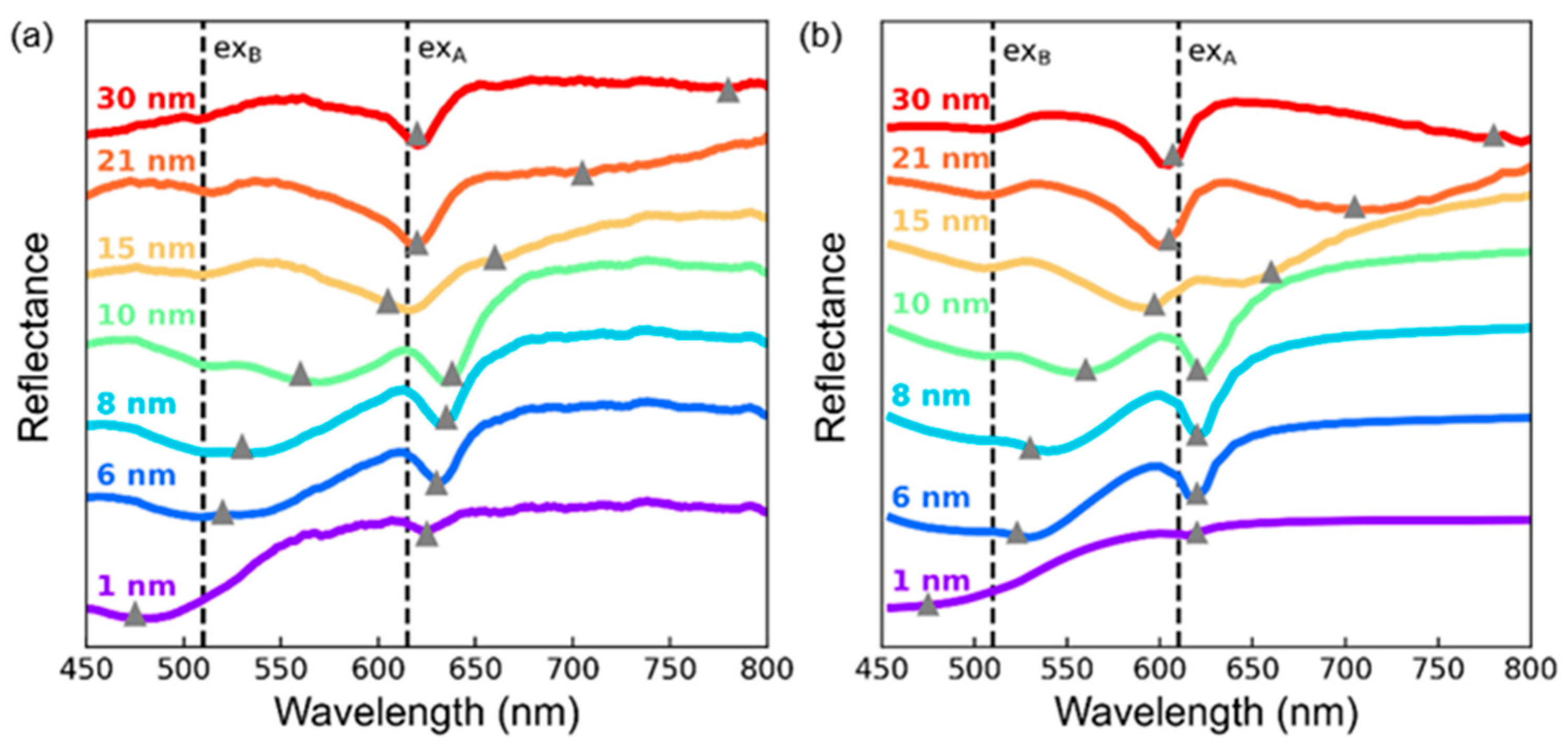
Figure 2a–e shows the calculated and measured reflectance spectra of WS
2 flakes. The calculated spectra were obtained using transfer matrix method (TMM) based on the refractive indices of the materials in the literature [
27,
28]. The spectra of stand-alone WS
2 flakes are also calculated for comparison with those of WS
2/SiO
2/Si and WS
2/Au (
Figure 2a). All the spectra exhibit local minima at 620 and 510 nm, which correspond to the A and B exciton resonance wavelengths of multilayer WS
2, respectively (see dashed lines in
Figure 2a–e) [
8,
9,
10,
23] WS
2 flakes with
dWS2 > 40 nm exhibit thickness-dependent reflectance dips in addition to the exciton resonance dips (
Figure 2a–c). These thickness-dependent reflectance dips originate from EP mode splitting since WS
2 multilayer flakes can work as optical cavities without external cavities [
8,
9,
10]. The EPs can be formed when the wavelengths of the exciton resonances and cavity modes are close to each other. For an intuitive understanding, FP cavity modes in dielectric thin films can be regarded as standing waves. Thus, the minimum
dWS2 for the FP cavity mode is expected to be either
λ/2
nWS2 or
λ/4
nWS2 (
n: real part refractive index of WS
2) [
26]. Considering the large refractive index of WS
2, the minimum
dWS2 allowing the FP resonance can be less than 100 nm. Wang et al. reported the EP mode splitting from WS
2 flakes with
dWS2 > 40 nm on glasses [
8]. Our results also show that the exciton–photon anticrossing occurs in sub-100-nm-thick WS
2 flakes (
Figure 2a–c). Interestingly, the EP-mediated reflectance dips appear in WS
2/Au even with
dWS2 < 40 nm (
Figure 2c). Zhang et al. reported similar thickness-dependent reflectance spectra from WS
2 multilayer flakes on Au thin films [
10].
Figure 2d,e shows the measured reflectance spectra of WS
2/SiO
2/Si and WS
2/Au with several
dWS2 values, respectively. These experimental data well reproduce the key features of the calculation results in
Figure 2b,c. The samples with
dWS2 of 50~60 nm show two EP-induced reflectance dips in both WS
2/SiO
2/Si and WS
2/Au, similar to others’ reports. [
8,
9,
10] Hereafter, the dips at the wavelength (
λ) < 600 nm and
λ > 600 nm will be called as UPB- and LPB-related dips, respectively (see gray circles in
Figure 2b–e). The UPB- and LPB-related reflectance dips also appear in the stand-alone flakes (
Figure 2a). This suggests that the EP mode splitting observed in the flakes with
dWS2 of several tens of nm is originated from the self-hybridization of the excitons and the FP cavity photons [
8,
9,
10] The reflectance spectra of WS
2/SiO
2/Si with
dWS2 = 8, 20, and 27 nm exhibit exciton resonance-mediated dips (see dashed lines in
Figure 2d). These spectra show a gradual increase in the reflectance at long wavelengths above 700 nm, which depends on the thickness of the SiO
2 layer (see
Figure S3 of Supplementary Materials). Thus, these long-wavelength features can be attributed to thin film interference in 300-nm SiO
2/Si substrates. In WS
2/Au with
dWS2 of 10 nm, a broad UPB-induced dip appears at 500 nm <
λ < 600 nm and a LPB-induced dip appears slightly above the A exciton resonance wavelength (see gray triangles in
Figure 2c,e). WS
2/Au with
dWS2 of 21 and 25 nm shows very broad UPB-mediated dips at
λ~600 nm and weak LPB-related dips at
λ > 600 nm (see gray triangles in
Figure 2c,e). These measured reflectance dips of WS
2/Au agreed well with the calculation data (
Figure 2c). This suggests that self-hybridized EP mode splitting can be formed in WS
2 flakes with
dWS2 much smaller than
λ/4
nWS2.
Figure 3a,b shows that the measured and TMM-calculated reflectance spectra of WS
2/Au with
dWS2 ≤ 30 nm well agreed with each other. This suggests that the samples were well prepared, as intended. In particular, the good agreement between the experimental and calculated results should be attributed to the ultrasmooth surface of the template-stripped Au thin films. In the calculations, the refractive indices of the bulk WS
2 in Ref. [
28] were used, since most of the flakes considered in this work were thicker than several layers. The UPB-related dips exhibit red-shift as increasing
dWS2 and they merge with the A-exciton dips. The LPB-related dips appear near the A exciton wavelength and exhibit red-shift as increasing
dWS2. From the measured and calculated data, the Rabi splitting energy of WS
2 flakes with
dWS2 < 50 nm on Au was estimated to be ~180 meV, which is somewhat smaller than those of flakes with
dWS2 > 50 nm reported in literature: ~270 meV in Ref. [
8] and ~235 meV in Ref. [
9] (see
Figure S4 of Supplementary Materials).
Figure 2c and
Figure 3a,b clearly show that the EP mode dips can appear in even sub-10-nm-thick WS
2 flakes on Au. Such thickness is much smaller than
λ/4
nWS2. Therefore, the simple analogy between the FP cavities and the standing waves in air columns cannot satisfactorily explain the minimum
dWS2 forming the EP modes in WS
2 flakes.
The electric field (E-field) distributions in WS
2/SiO
2/Si and WS
2/Au can be obtained using finite-difference time-domain (FDTD) simulation, as shown in
Figure 4a–d. The horizontal axis,
z, represents the position along the direction perpendicular to the sample surface. The origins of
z were chosen at the WS
2/SiO
2 and WS
2/Au interfaces for WS
2/SiO
2/Si and WS
2/Au, respectively. The regions between the dashed lines represent the WS
2 flakes with
dWS2 = 70 nm for
Figure 4a,b and
dWS2 = 20 nm for
Figure 4c,d. The left sides of the WS
2 regions indicate the underlying SiO
2 (300 nm) and Au (100 nm) layers for WS
2/SiO
2/Si (
Figure 4a,c) and WS
2/Au (
Figure 4b,d), respectively. The right sides of the WS
2 flakes indicate air. The E-field distributions were obtained at wavelengths where the local minima of the reflectance appear (
Figure 2b,c). The field distribution for WS
2(70 nm)/SiO
2/Si at
λ = 580 nm, corresponding to UPB, is similar to the fundamental-mode standing wave in a pipe opened at both ends (
Figure 4a). At
λ = 650 nm, corresponding to LPB, the WS
2/SiO
2 interface looks like the antinode of a standing wave, but the other antinode is in air rather than the WS
2 surface. The field distribution for WS
2/Au can be compared to the standing wave pattern of a one-side-closed air column. In the cases of WS
2(70 nm)/Au at
λ = 555 (UPB) and 630 nm (LPB), the WS
2/Au interface is similar to the node of a standing wave, but the antinode is in air (
Figure 4b). The E-field exponentially decays in the Au layer due to the absorption and the decay length is determined by the penetration depth of light in Au (for example, 50 nm at
λ = 600 nm) [
29].
The
dWS2 of 20 nm is only ~1/10 of the wavelength of visible light, even if the large refractive index of WS
2 (4~5) is considered. Thus, the magnitude of the E-field does not change much in the 20-nm-thick WS
2 flakes (
Figure 4c,d). As shown in
Figure 4c, a large E-field appears in the 20-nm-thick WS
2 flake on SiO
2/Si under 600-nm-wavelength light illumination. Since the absorption is proportional to the square of the E-field, the large E-field increases (reduces) the absorption in the flake (reflectance), as shown in
Figure 2b,d. In WS
2(20 nm)/Au, the local minima in the reflectance appear at
λ = 600 and 700 nm (
Figure 2c). The magnitude of the E-field in the flake at
λ = 600 nm is smaller than that at
λ = 700 nm (
Figure 4d). Since the optical absorption depends on the imaginary part of the permittivity of the medium as well as the E-field, the smaller reflectance of WS
2 (20 nm)/Au at
λ = 600 nm seems to result from the very large absorption coefficient of WS
2 near the exciton resonance wavelength. At
λ = 700 nm (LPB), the relatively large E-field increases the absorption in the WS
2 flake, resulting in a broad reflectance dip at
λ = 700 nm (
Figure 2c). Obviously, the cavity modes in WS
2/Au with
dWS2 < 40 nm are distinct from typical FP resonance modes, which can be regarded as standing waves.
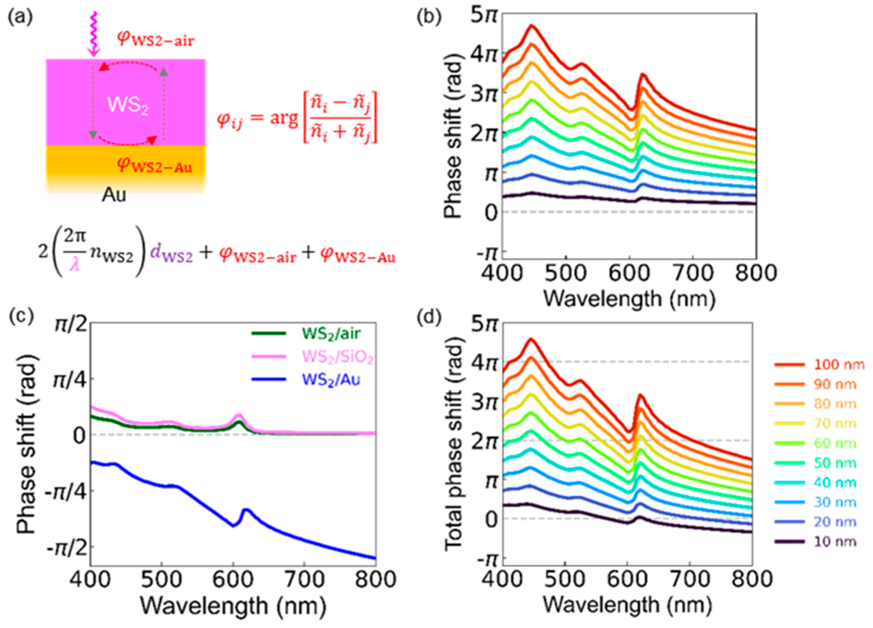
As illustrated in
Figure 5a, three kinds of optical phase shifts need to be considered to understand the reflectance spectra of WS
2/SiO
2/Si and WS
2/Au. The spectra of the multilayers can be explained by superposition of light reflected at each interface, i.e., multiple-beam interference [
26]. First, the propagation-related phase shift of light,
φWS2, is given by
, as shown in
Figure 5b. Clearly,
φWS2 increases with increasing
dWS2. Notably,
φWS2 of a 50-nm-thick WS
2 flake becomes larger than 2π.
nWS2 is as large as 4~5 in the visible wavelength range and, therefore, the propagation of light in the WS
2 flake with a thickness of only about ~1/10 of the vacuum wavelength results in a large
φWS2 [
23]. The Fresnel coefficient of the reflected light,
rij, is
(
ni and
nj are the refractive indices of the two media at the interface) [
26]. If
ni and
nj are real, then
rij, is also real and the phase of
rij can be either 0 (
rij ≥ 0) or π (
rij < 0). However, the phase of
rij can differ from either 0 or π for complex
ni and
nj. The Fresnel coefficient-related phase shifts at the WS
2/air (
φAir), WS
2/SiO
2 (
φSiO2), and WS
2/Au (
φAu) interfaces are shown in
Figure 5c. The optical phase shifts largely vary as a function of wavelength, depending on the complex refractive indices of WS
2 and Au. The magnitude of
φAu is much larger than that of
φAir and
φSiO2 over a broad wavelength range since the complex refractive index of Au is very large [
27,
29].
Figure 5d shows the total round-trip phase shift of light in WS
2/Au,
φTotal, which is the sum of the interfacial Fresnel coefficient-related contributions (
φAir and
φAu) as well as the propagation-related change (
φWS2). When
φTotal is equal to integer multiples of 2π, WS
2/Au can form resonant cavity modes. Such resonant modes boost the optical absorption in the WS
2 flakes, as featured as local minima in the optical reflectance spectra. The intersection points of the
φTotal and 2π(integer) curves represent the resonant cavity mode wavelengths for WS
2/Au. The intersection points in
Figure 5d agree well with the local minima in the calculated and measured spectra in
Figure 2c,e. For
dWS2 > 40 nm,
φWS2 is larger than 2π at a certain wavelength, giving rise to the FP resonance modes and resulting EP-induced reflectance dips.
Figure 5d also shows that the resonant modes can appear for
dWS2 < 30 nm. For example, WS
2/Au of
dWS2 = 10 nm possesses intersection points near
λ = 600 nm, close to the A exciton resonance wavelength of WS
2. As a result, the reflectance spectra of sub-10-nm-thick WS
2 flakes on Au exhibit clear features of UPB and LPB modes, as shown in
Figure 2c and
Figure 3a,b. It should be noted that
φWS2 alone cannot enable the resonant cavity mode in WS
2/Au of
dWS2 < 10 nm (
Figure 5b). Since the negative
φAu can reduce
φTotal to zero at certain wavelengths, WS
2/Au enables the coupling of excitons and cavity photons (
Figure 5c,d). The considerable contribution of the interface phase shift can explain why the E-field distributions in WS
2/Au are distinct from the waveforms of simple standing waves (
Figure 4b,d).
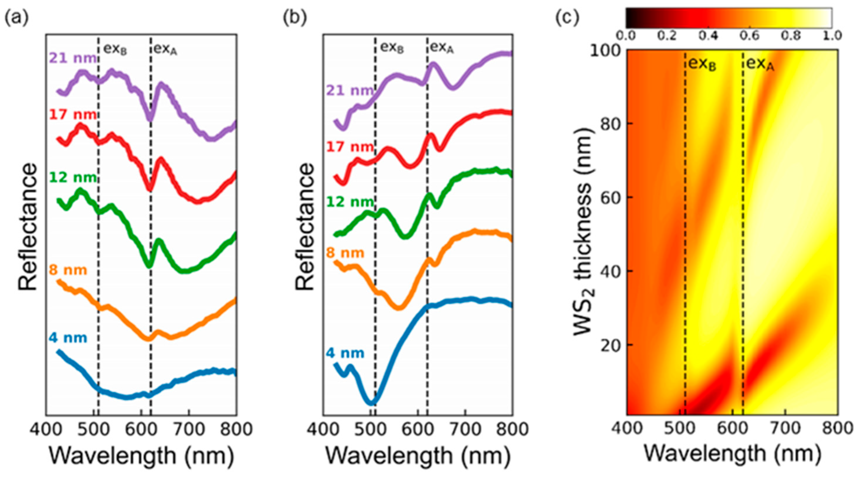
Figure 6a,b shows the measured reflectance spectra of WS
2 flakes on SiO
2/Si substrates with
dWS2 < 30 nm before and after deposition of 30-nm-thick Au thin films, respectively. The top Au layers significantly modify the reflectance spectra of the WS
2 flakes. Such very thin flakes without Au thin films cannot exhibit the EP mode splitting, and there are only exciton-related dips in the reflectance spectra (
Figure 2b and
Figure 6a). However, the Au-coated flake exhibits additional reflectance dips in addition to the exciton-related dips, indicating the self-hybridized EP modes (
Figure 6b). Since the penetration depth of Au at
λ = 600 nm is 50 nm, the 30-nm-thick Au thin films allow the transmission of incident light to the WS
2 flakes and the formation of optical cavity modes [
29]. The TMM-calculated 3D reflectance plots of Au(30 nm)/WS
2/SiO
2/Si samples in
Figure 6c clearly show the exciton–photon anticrossing behaviors for not only
dWS2 > 40 nm but also
dWS2 < 40 nm, similar to WS
2/Au (
Figure 2c and
Figure 3a,b). The additional dips in the measured spectra (
Figure 6b) agree well with those in the calculations (
Figure 6c). These experimental and calculated results suggest that the contribution of the large optical phase shifts at the Au/WS
2 interface is crucial for the formation of EPs in WS
2 flakes with
dWS2 <
λ/4
nWS2. Many TMDs possess large real and imaginary parts of refractive indices [
11,
12,
13,
14,
15,
30], and hence the EP modes are expected in other kinds of very thin TMD layers. Furthermore, strong electronic interactions [
31] as well as remarkable plasmonic effects [
7,
10] at TMD/metal interfaces can give rise to emergent physical phenomena of TMD/metal systems.


