Article

Top-Emitting Active-Matrix Quantum Dot Light-Emitting Diode Array with Optical Microcavity for Micro QLED Display

1
Ph.D. Program in Prospective Functional Materials Industry, College of Engineering, National Tsing Hua University, Hsinchu 30013, Taiwan
2
Department of Materials Science and Engineering, National Tsing Hua University, Hsinchu 30013, Taiwan
3
Technology Development Division, Innolux Corporation, Miaoli 35053, Taiwan
4
Hsinlight Inc., South Campus, National Tsing Hua University, Hsinchu 30013, Taiwan
*
Author to whom correspondence should be addressed.
Nanomaterials 2022, 12(15), 2683; https://0-doi-org.brum.beds.ac.uk/10.3390/nano12152683
Submission received: 29 June 2022 / Revised: 19 July 2022 / Accepted: 27 July 2022 / Published: 4 August 2022

Abstract

:
An electroluminescent quantum-dot light-emitting diode (QLED) device and a micro QLED device array with a top-emitting structure were demonstrated in this study. The QLED device was fabricated in the normal structure of [ITO/Ag/ITO anode]/PEDOT:PSS/PVK/QDs/[ZnO nanoparticles]/Ag/MoO3, in which the semi-transparent MoO3-capped Ag cathode and the reflective ITO/metal/ITO (IMI) anode were designed to form an optical microcavity. Compared with conventional bottom-emitting QLED, the microcavity-based top-emitting QLED possessed enhanced optical properties, e.g., ~500% luminance, ~300% current efficiency, and a narrower bandwidth. A 1.49 inch micro QLED panel with 86,400 top-emitting QLED devices in two different sizes (17 × 78 μm2 and 74 × 40.5 μm2) on a low-temperature polysilicon (LTPS) backplane was also fabricated, demonstrating the top-emitting QLED with microcavity as a promising structure in future micro display applications.

Graphical Abstract

1. Introduction

Colloidal quantum dots (QDs) have attracted significant attention in various applications, such as energy harvesting, sensing, and displays, because of their irreplaceable optical properties such as high quantum yield (QY), wide absorption range, tunable emission wavelength, and high-purity color [1,2,3,4]. For liquid crystal displays (LCDs), QDs can improve their color gamut by simply introducing QDs in various application forms, including QD films [5,6,7], QD light guide plates [8], QD color converters [9,10,11], and QD-converted light-emitting diodes (QD-LEDs) [12,13,14,15,16,17]. A QD-enhanced LCD can be called a QD-LCD. On the other hand, electroluminescence (EL)-based QD light-emitting diodes (QLEDs) [18,19,20,21,22,23,24] can work without a backlight and may be called a self-emitting QLED or EL-QLED. A self-emitting QLED has excellent color performance, such as narrow and adjustable emission bandwidth and wavelength, viewed as next-generation lighting and display technology. Compared with other displays, QLED has higher image contrast and a faster response than QD-LCD [25], as well as a broader color gamut coverage than organic light-emitting diode (OLED) or micro-LED [26,27,28]. Furthermore, the solution-based fabrication process of QLED offers the advantages of large-area applications at a low manufacturing cost.
Both passive-matrix (PM) and active-matrix (AM) driving electrode systems may be used to realize display applications, where the latter is beneficial for a larger display area or higher resolution. In terms of AM-based QLED, the conventional device design is bottom-emitting, where the light emission is extracted from the glass substrate side [29,30,31,32]. However, the opening of the bottom-emitting device and the light intensity are limited by the opaque thin-film transistor (TFT) circuit in the AM backplane. Hence, a higher operating current density is required to produce sufficient display brightness, which consumes more energy and reduces the operation lifetime of QLED devices. Instead, the top-emitting structure is more suitable for a high-resolution AMQLED display [33]. In the previous studies on top-emitting QLED (TEQLED), a semi-transparent metal electrode (Ag) served as the top electrode, allowing light to pass through it, while Al or Ag was employed as a reflective bottom electrode that increased light extraction [33,34,35,36]. Ag has a high reflectance and a low absorbance in the visible wavelength range, and it has been commonly utilized as a bottom electrode that simultaneously reflects light to the top side. However, Ag has a low work function (~4.3 eV) and is not beneficial to hole injection in the normal device structure [34,37]. Furthermore, the reflective bottom electrode and the semi-transparent top electrode may form an optical microcavity, significantly affecting the light coupling and interference in the devices [34,38,39,40]. Therefore, the optical microcavity effect associated with the thickness of each device layer should be considered in TEQLEDs.
This study demonstrates a high-resolution monochrome AMQLED with a top-emitting structure using a conventional low-temperature polysilicon (LTPS) backplane used for OLEDs. The TEQLED is fabricated in a normal structure, where an ITO/Ag/ITO (IAI) multilayer electrode acts as a reflective bottom anode and a thin Ag film capped with MoO3 serves as the semitransparent top cathode. By adjusting the thickness of the ZnO layer and QD layer to form an optical microcavity, TEQLEDs can exhibit fivefold the maximum luminance (~129,200 cd·m−2) and threefold higher current efficiency (~28.4 cd·A−1) than bottom-emitting QLED (BEQLED).

2. Experimental Section

2.1. Fabrication of TEQLED

ITO/Ag/ITO-coated glass substrate was ultrasonically cleaned in DI water, acetone, and IPA for 15 min sequentially. Then, the substrate was treated by UV ozone to modify the wettability and the work function. The PEDOT:PSS solution (AI 4083) was filtered using a 0.45 μm Nylon filter before being spin-coated on a substrate at 3000 rpm for 50 s. The substrate was transferred to a nitrogen-filled glovebox and annealed at 140 °C for 20 min. PVK (Mw 25,000–50,000 g·mol−1, 5 mg·mL−1 in toluene) was spin-coated onto HIL and annealed at 140 °C for 20 min, resulting in a 17 nm thick HTL. The QDs (G-QD-1, 0.5 nm shell thickness, wavelength 529 nm/FWHM 34.1 nm/PLQY 80%/EL-QD 1-low driving voltage, provided from Hsinlight Inc., Taiwan) was spin-coated at 2000 rpm for 40 s and annealed at 80 °C for 10 min; the concentration of QD solution was adjusted from 5 mg·mL−1 to 20 mg·mL−1 for the desired thickness. ZnO NPs (in IPA) were spin-coated at 2000 rpm for 40 s and annealed at 60 °C for 10 min, the concentration of ZnO solution was adjusted from 10 mg·mL−1 to 30 mg·mL−1 for the desired thickness. Finally, the semi-transparent cathode consisting of Ag (30 nm) and MoO3 (30 nm) was thermally deposited under a high vacuum (<8 × 10⁻⁶ torr). A cover glass and the UV-curable resin were used to encapsulate the device. The synthesis of ZnO nanocrystals was described in our previous paper [41]. For comparison, devices prepared with two other alloyed ZnCdSeS QDs with different shell thicknesses (G-QD-2/1.1 nm shell thickness/wavelength 523 nm/FWHM 20.5 nm/PLQY 65% and G-QD-3/1.6 nm shell thickness/wavelength 521 nm/FWHM 17.7 nm) were also fabricated using the same processes and parameters. The ligand type of all QDs was oleic acid.

2.2. Characterizations

Photoluminescence (PL) spectra and electroluminescence (EL) spectra were measured by a spectrofluorometer (Edinburgh FS5 from England). Optical absorption was measured by a UV/Vis/NIR spectrophotometer (Jasco V-770 from Japan). Surface morphology of the cathode was observed by field-emission scanning electron microscopy (FESEM, Hitachi SU8010 from Japan). Cross-sectional transmission electron microscopy (TEM) images and the line-scan profile of energy-dispersive X-ray spectroscopy were acquired on a high-resolution TEM (HRTEM, JEOL JEM-F200 from Japan). The device cross-section sample was prepared with a focused-ion-beam (FIB) system (SII NANOTECH SMI2050 from Japan) equipped with a Ga+ ion beam. The valence band maximum (VBM) of QDs was identified by ultraviolet photoelectron spectroscopy (UPS, ULVAC-PHI PHI 5000 Versaprobe II from Japan) with a UV source (He I α, 21.22 eV). The Tauc plot derived from the absorption spectrum was used to analyze the optical bandgap of QDs. The current density–voltage–luminance characteristics of QLEDs were measured by a source meter unit (SMU, Keithley 2450 from USA) and a luminance meter (TOPCON BM-9A from Japan). The contact angle of water on Ag and ITO was acquired from a contact angle analyzer (FTA125 from USA).

3. Results and Discussion

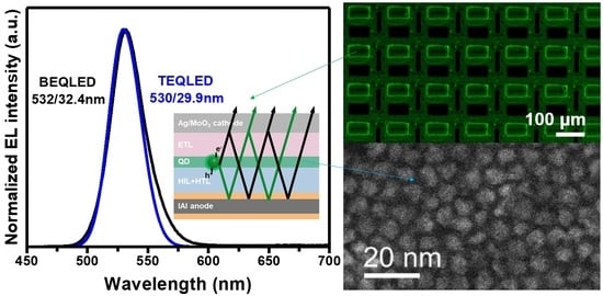
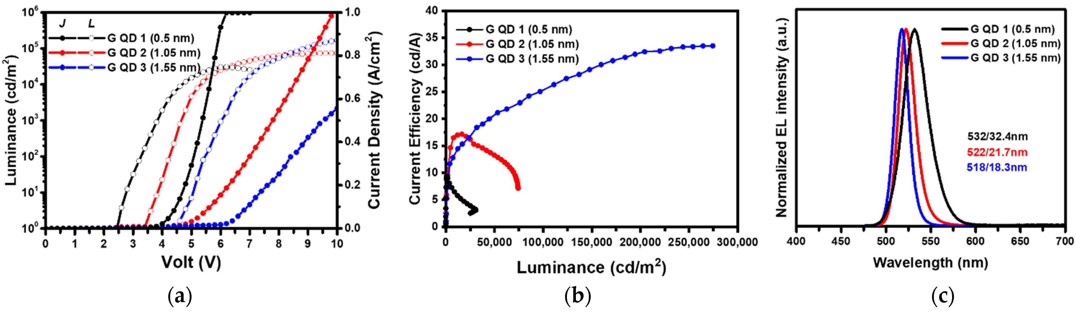
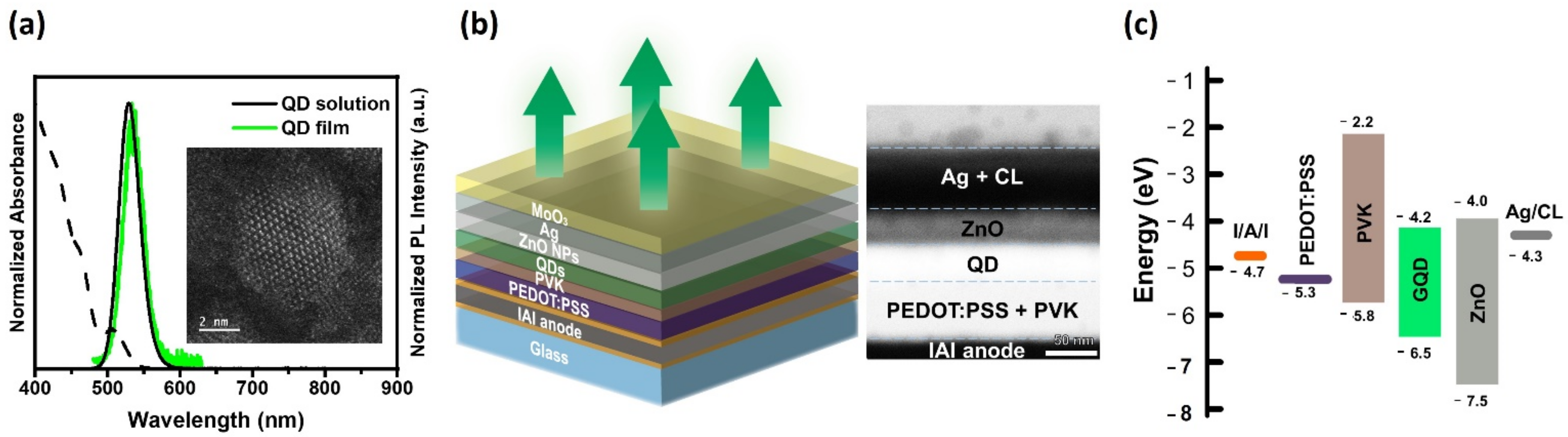
3.1. Selection of Appropriate Type of QDs for AMQLED Array and Panel

To operate a QLED device array, the QLED driving conditions, such as the turn-on voltage and current–voltage relation, are much more important than for a single QLED device. Hence, the selection of a proper type of QDs is one of the keys. Otherwise, the QLED device array may not correctly work. For a QLED device array applied to a display panel, the driving condition and display quality (e.g., wavelength, bandwidth, and performance) of every QLED device are significantly influenced by the external circuit and driver. In terms of AMQLED, a conventional OLED display driving system can be utilized to drive an AMQLED panel, whereby the QD emitting layer may necessarily be similar to the organic emitting layer in terms of device properties. In general, a lower driving voltage (<5 V) is required for existing AM LTPS-TFT backplanes to drive every emitting device. Three types of green alloyed ZnCdSeS QDs with different shell thicknesses (0.5 nm/G-QD-1, 1.1 nm/G-QD-2, and 1.6 nm/G-QD-3, Figure S1) were first fabricated in the conventional BEQLED structure to evaluate their applicability. Figure 1 shows the current density–voltage–luminescence and current efficiency–luminance (CEL) characteristics, as well as the EL spectra, of devices with G-QD-1, G-QD-2, and G-QD-3. The turn-on voltage (Von) increased from 2.5 V to 4.6 V with increasing shell thickness from 0.5 nm to 1.6 nm, indicating that carrier injection was more efficient for the thinner-shelled QDs. With thicker-shelled QDs, the devices showed higher current efficiency and luminance, representing better carrier confinement at the high electric field contributed by the thick shell. In particular, the device with G-QD-3 possessed the maximum luminance and a current efficiency of over 280,000 cd·m−2 and 33 cd·A−1, respectively. Although thick-shelled QDs may have a higher device performance, a high operating voltage range is not suitable for the current LTPS-TFT backplanes. Therefore, G-QD-1 was used to study the device and panel properties of AMQLED display panels.

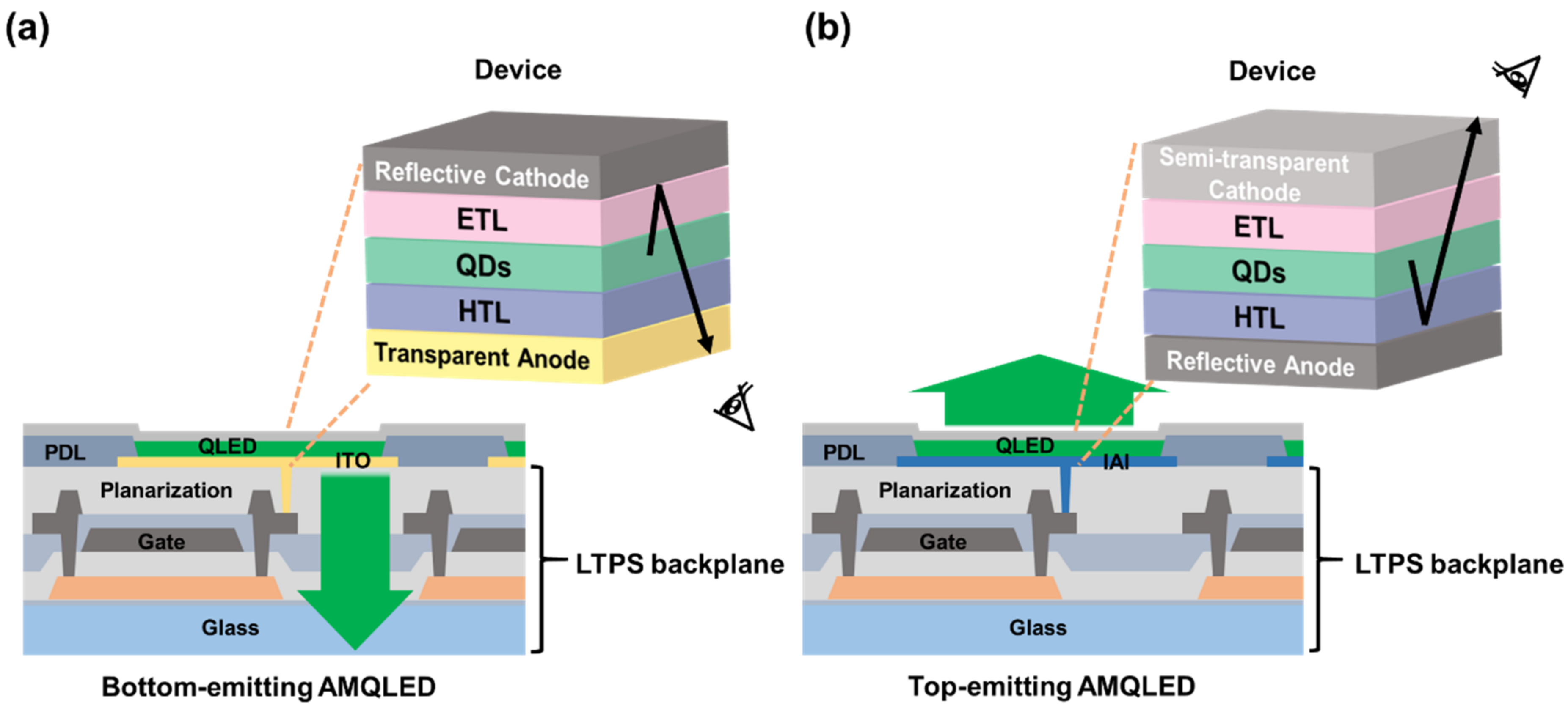
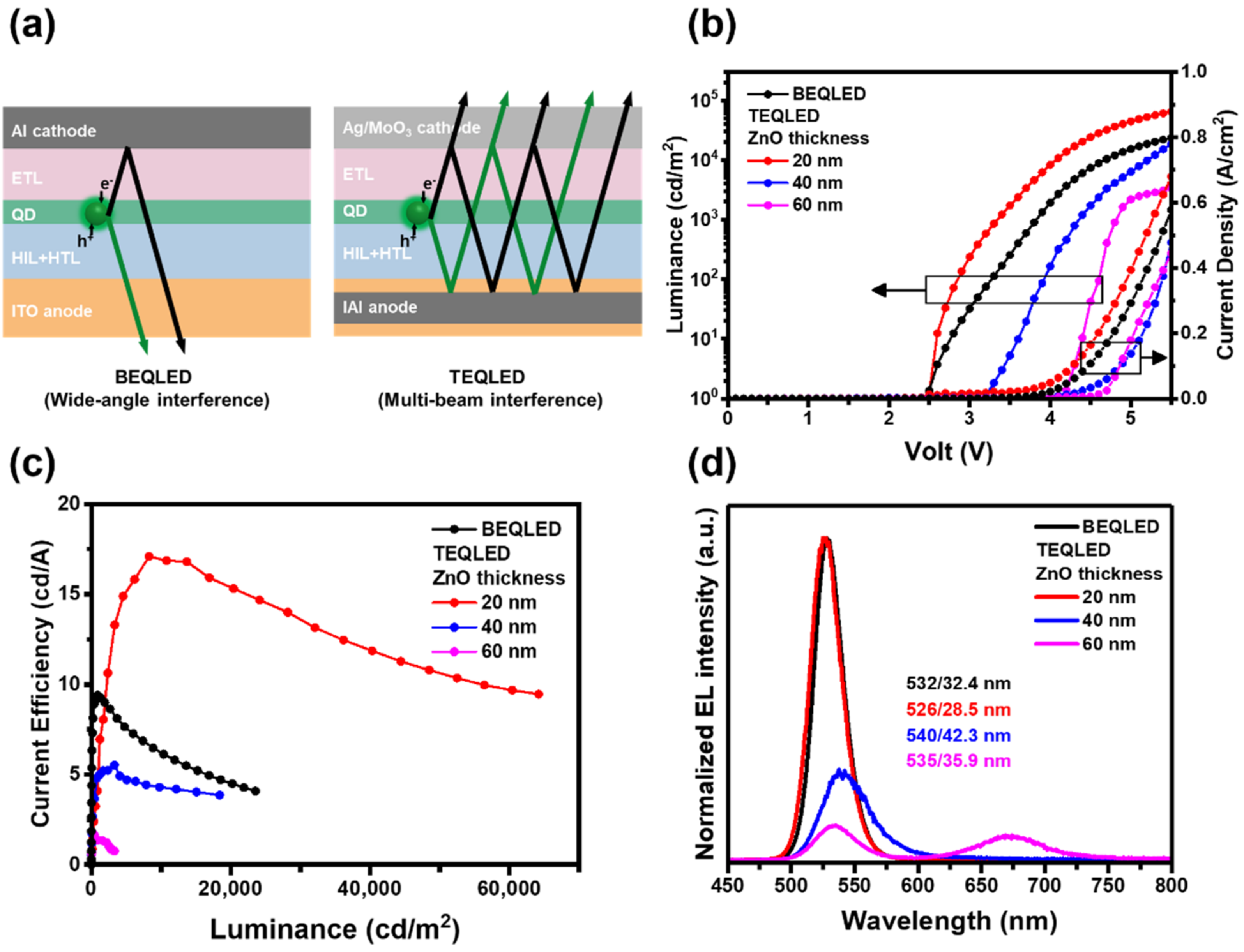
3.2. QLED with the Top-Emission Structure

Conventional QLED devices are generally fabricated in a so-called normal device structure with bottom emission, e.g., glass substrate/ITO anode/hole-transporting layer (HTL)/QDs/electron-transporting layer (ETL)/metal cathode, in which the emitting light can be extracted from the glass substrate side. For an AM display panel with a bottom-emitting structure, the ITO anode is prepared on a TFT backplane to control every single emitting device (i.e., pixel). Therefore, the emission intensity of pixels is restricted by the opening space (also called the aperture size) of the TFT backplane involving electrodes and wiring, limiting the pixel size and display resolution, as schematically illustrated in Figure 2a. On the other hand, the top-emitting device structure has a larger aperture size, allowing a higher emission intensity, which is more suitable for a higher-resolution AM-based QLED display panel (e.g., >150 ppi), as shown in Figure 2b. With a top-emission design, the light generated by the QLED devices passes through the top cathode side; hence, the bottom anode must be reflective to increase the light extraction efficiency.
Figure 3a shows the optical absorption and PL spectra of G-QD-1. The emission wavelength and full width at half maximum (FWHM) of the QDs in octane were 529 nm and 34.1 nm, respectively. The PL spectrum of the spin-coated QD film showed a red-shifted emission peak and a narrower FWHM (534 nm/32.4 nm) caused by Förster resonance energy transfer (FRET) in a densely packed QD film [42]. A cross-sectional TEM image of the top-emitting QLED (TEQLED), together with its schematic structure, is shown in Figure 3b. The TEQLED was fabricated in a normal structure, i.e., [ITO/Ag/ITO]/PEDOT:PSS/PVK/QDs/[ZnO NPs]/[semi-transparent Ag]/MoO3, where [ITO/Ag/ITO], PEDOT:PSS, PVK, QDs, ZnO NPs (nanoparticles), semi-transparent Ag, and MoO3 were the reflective anode, hole injection layer (HIL), HTL, emission layer (EML), ETL, cathode, and capping layer, respectively. Figure 3c shows the energy band diagram of the TEQLED, in which the QD energy level was estimated from the ultraviolet photoelectron spectroscopy (UPS) spectrum and Tauc plot (Figure S2).

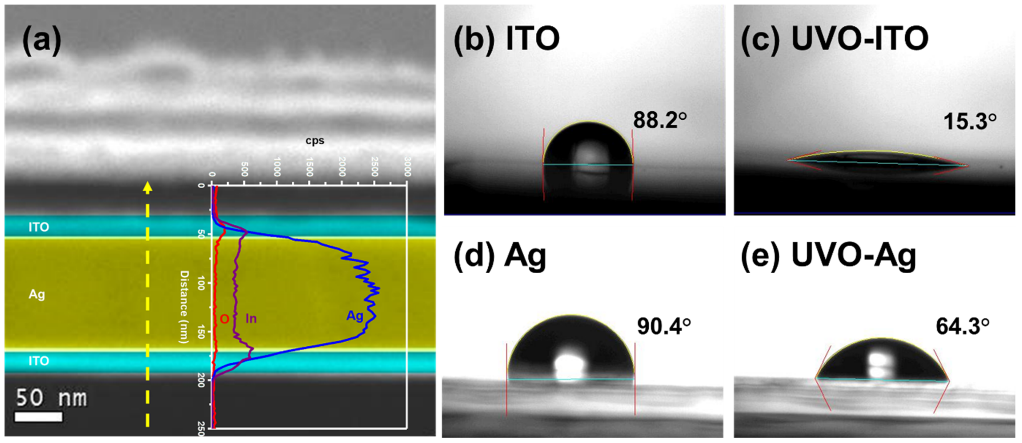
3.3. Fabrication of Bottom Reflective Anode in the IAI Structure

A pure Ag film is generally used as a bottom reflective electrode because of its high conductivity and reflectance. Nevertheless, the metal film is relatively less hydrophilic even after a surface modification. Instead, a tri-layered transparent conductive oxide/metal/transparent conductive oxide composite film, i.e., ITO/Ag/ITO (IAI) with a thickness of 20 nm/110 nm/20 nm, was adopted as the reflective anode (Figure 4a). Compared with the pure Ag film, the IAI anode has the advantages of better material stability and enhanced optical reflection because of ITO protection [45]. Moreover, the IAI anode has more surface processability. It can be feasibly treated with UV/ozone to ensure a better match in the work function and higher chemical compatibility with the subsequent HIL layer [23,46]. For example, the ITO surface of IAI became more hydrophilic after UV/ozone treatment compared with the UV/ozone-treated Ag film, which was still relatively more hydrophobic and could affect the film deposition of PEDOT:PSS (Figure 4b–e).

3.4. Top Ag Cathode with MoO3 Capping Layer

Thermally evaporated Ag film was prepared as the semi-transparent top cathode instead of sputtering-based transparent conductive oxides because the latter process may degrade the QD layer [47,48]. To prepare a transparent metal electrode, ultrathin (e.g., <10 nm) Ag is generally necessary. Unfortunately, Ag easily forms a discontinuous film or aggregate-like particulate morphology on a substrate, significantly affecting the optical properties (e.g., light scattering) and the carrier injection [49]. In the current QLED panels, a relatively thicker Ag cathode (~ 30 nm) was prepared to ensure that the device worked correctly because the TFT panels could not appropriately work with a thinner Ag film. However, a thicker Ag cathode could slightly reduce the optical transmittance of the QLED pixels. Moreover, a refractive index mismatch between the Ag cathode and the air decreased the device emission intensity. Consequently, an additional MoO3 capping layer was introduced to clad the Ag cathode to improve light extraction [50,51]. MoO3 has a high refractive index and a low extinction coefficient [52,53]. By thermally depositing a 30 nm MoO3 capping layer, the transmittance of Ag film could be increased (Figure S3). With the MoO3 capping layer, TEQLEDs showed an 81% improvement in the current efficiency (8.8 cd·A−1 to 15.9 cd·A−1, Figure S4). In addition, some current leakage in the TEQLED without a capping layer was observed, which could be explained by the poor Ag film quality (Figure S5). It has been reported that a MoO3 capping layer can improve the Ag film morphology and inhibit Ag grain agglomeration [54,55].

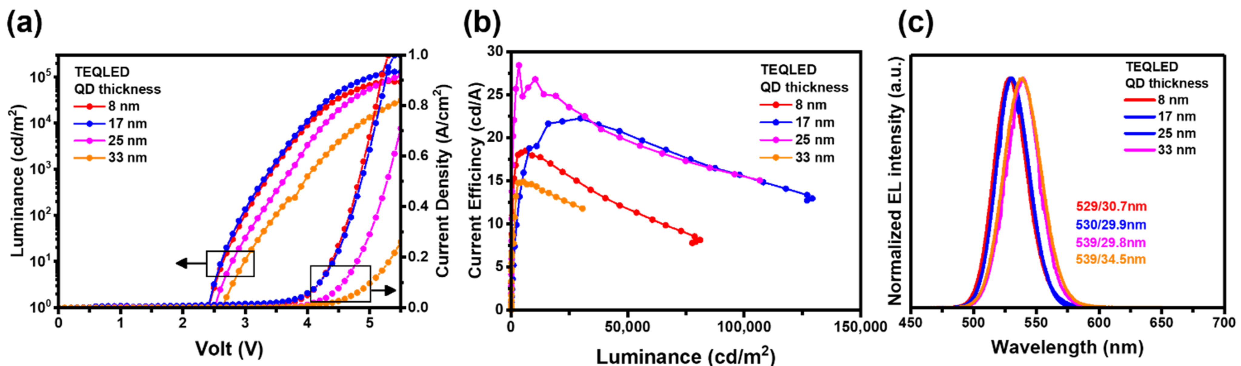
3.5. Design of Optical Microcavity for TEQLEDs

The optical length of top-emitting devices significantly affects their optical performance. Sandwiched by an IAI reflective anode and a semi-transparent Ag cathode, a microcavity structure was prepared in the TEQLEDs. Figure 5a schematically shows the two interference modes occurring in BEQLED and TEQLED, i.e., wide-angle and multi-beam interference. The constructive interference conditions are given below [56].
m × 2 π = 2 π 2 n i d i cos θ λ φ anode   ( wide - angle   interference ) ,
m × 2 π = 2 π 2 n i d i cos θ λ φ anode φ cathode   ( multi - beam   interference ) ,
where n and d are the refractive index and the thickness of the layer, respectively. φ is the reflective phase shift of the electrode. The structure consists of a highly reflective back mirror electrode and a transparent output mirror electrode, forming an optical microcavity [57]. With an appropriate film thickness and tailored design, the microcavity can enhance the device brightness and the color purity, which is beneficial for energy-efficient displays with a high color gamut [58]. The resonant wavelength of the microcavity mainly depends on the optical length. If the QD emission wavelength meets the resonant wavelength of the microcavity, constructive interference can enhance the light emission intensity. Since the Ag/MoO3 cathode had higher reflectance than ITO, the enhancement in TEQLED was more significant. Table 1 shows a comparison of QLED devices prepared in the bottom-emission and top-emission structure.
To investigate the resonant wavelength of the microcavity, the device optical length was varied by the ZnO layer thickness, which could be feasibly adjusted [59]. Figure 5 gives the JVL and CEL characteristics, as well as EL spectra, of TEQLEDs with 20, 40, and 60 nm ZnO thickness. The 20 nm ZnO TEQLED had the lowest Von (~2.5 V), while the 40 nm ZnO and 60 nm ZnO TEQLEDs had a higher Von of 3.2 V and 4.2 V, respectively (Figure 5b). In addition, the 20 nm ZnO TEQLED had the highest efficiency of 17 cd·A−1, but the device efficiency decreased with increasing ZnO thickness (Figure 5c). Figure 5d shows the EL spectra of TEQLEDs operated at 2 mA. The TEQLEDs with 20, 40, and 60 nm ZnO layers had an EL wavelength/FWHM of 526 nm/28.5 nm, 540 nm/42.3 nm, and 535 nm/35.9 nm, respectively. The 20 nm ZnO TEQLED had a shorter EL wavelength and narrower bandwidth compared with the PL spectra of QDs in either solution or film form (wavelength/FWHM = 529 nm/34.1 nm and 534 nm/32.4 nm, Figure 3a). This fact indicates that a proper design of microcavity resonance can improve the optical property of TEQLEDs.
However, the device with a 40 nm or 60 nm ZnO layer had a broader and red-shifted EL curve. For the device with a 60 nm ZnO layer, a deep-red emission band appeared at 675 nm, ascribed to the red emission of PVK amplified by the microcavity [60]. Accordingly, the inappropriate optical length may affect the device performance of TEQLEDs. Table 2 gives a summary of device data for the TEQLEDs with different ZnO thicknesses.
A control BEQLED sample was also fabricated with the structure of ITO/PEDOT:PSS (40 nm)/PVK (17 nm)/QDs (33 nm)/ZnO (20 nm)/Al (100 nm) for reference (black curves in Figure 5b–d). The Von of the BEQLED was 2.5 V, corresponding to the optical bandgap of green QDs (2.34 eV). The low Von value reveals that carriers could be smoothly injected into the QDs through the carrier transport material that was energy level-matched. The current efficiency of BEQLED showed a max value of 9.4 cd·A−1 at a luminance of 1000 cd·m−2. Furthermore, the EL spectrum of the BEQLED (wavelength/FWHM = 532 nm/32.4 nm) was somewhat similar to the PL spectrum of the QD film (wavelength/FWHM = 534 nm/32.4 nm, Figure 3a), suggesting that no optical resonance effect existed in the bottom-emission structure.
The effect of the thickness of QD layer was also studied to improve the device properties of TEQLEDs. Devices with 30 nm ZnO were first prepared to form a resonant wavelength close to ~534 nm, meeting the display criteria of green wavelength. An increase in the QD thickness slightly raised the Von from 2.5 V to 2.7 V and reduced the current density, as shown by the JVL characteristics in Figure 6a. The result may be explained by a thicker QD layer with a large amount of long alkyl chain ligands (i.e., oleic acid), leading to higher resistance in the device. For TEQLEDs with a 17 or 25 nm thick QD layer, the device luminance could reach over 100,000 cd·m−2, which is an approximately fivefold enhancement compared with BEQLED. As a result, the maximum current efficiencies of the TEQLEDs were enhanced to 20–30 cd·A−1 (Figure 6b). In addition, the FWHMs of TEQLEDs with 8, 17, and 25 nm thick QD layers were all narrower than those of BEQLED, indicating that the microcavity effect with constructive interference could also reduce the bandwidth and improve the color purity, as shown by the EL spectra in Figure 6c.
Moreover, when the thickness of QD layer was increased from 8 to 33 nm, the EL emission peak red-shifted from 529 to 539 nm, suggesting that the resonant wavelength of the cavity moved to a longer value because of increasing cavity length. The TEQLED with a 25 nm QD layer had the highest current efficiency of ~28 cd·A−1 and the max brightness of ~106,700 cd·m−2 at the EL wavelength of ~539 nm. The relatively low current efficiency of TEQLED with a 33 nm QD layer is attributable to the poor carrier injection and destructive interference in the microcavity structure. Table 3 summarizes the device performance and the QD thickness of TEQLEDs.

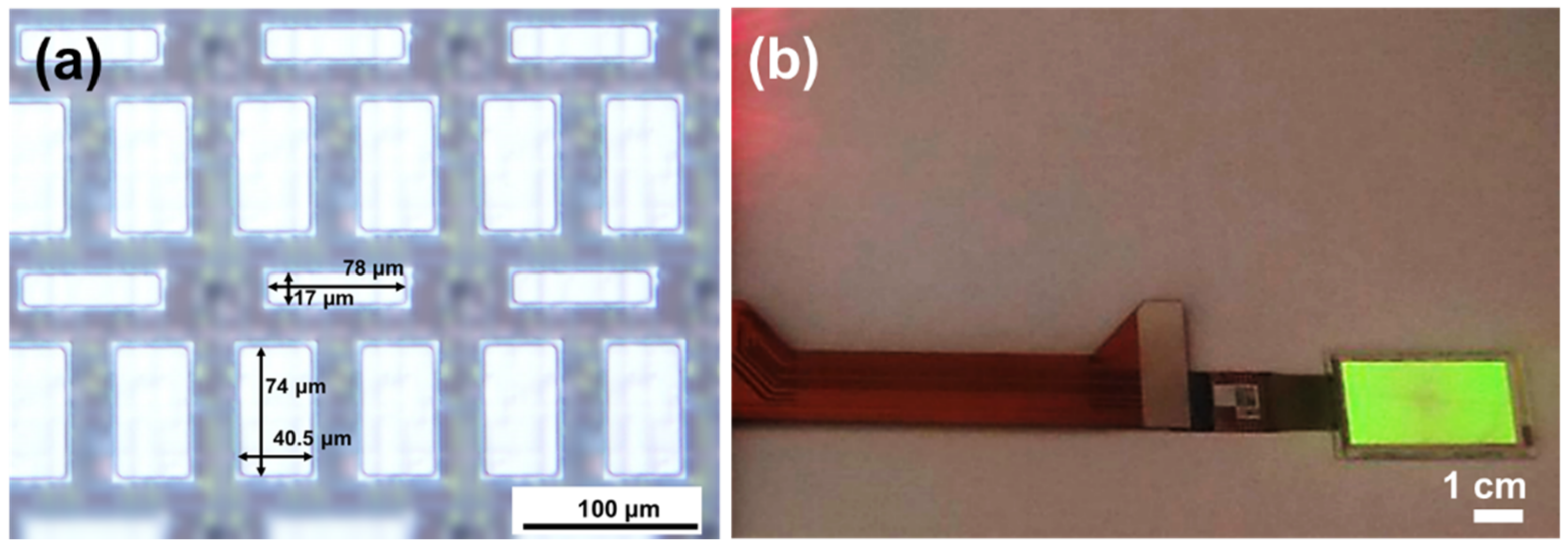
3.6. QLED Array Fabricated on a 1.49 Inch LTPS-TFT Substrate for Micro Display

The top-emitting QLED structure was further fabricated into a micro device array to demonstrate its potential application in a micro display panel. A 1.49 inch TFT glass backplane with an aperture ratio of 36.8% was employed as a substrate, as shown in Figure 7a. The pixel-defining area of the backplane had two different dimensions (17 × 78 μm2 and 74 × 40.5 μm2). Fabrication of the micro QLED device array on the TFT backplane followed the same spin-coating-based process of a single QLED device. Figure 7b presents a fabricated QLED panel composed of 86,400 green top-emitting devices. The QLED panel could be operated in the range between 3 V and 5 V, exhibiting promise for application in a high-resolution micro monochrome QLED display.

4. Conclusions

A 1.49” top-emitting micro AMQLED array with an optical microcavity was demonstrated in this study. The QLED device was fabricated in the top-emitting normal structure of [ITO/Ag/ITO]/PEDOT:PSS/PVK/QDs/ZnO/[Ag-MoO3]. The MoO3-capped Ag cathode and the ITO/metal/ITO (IMI) anode formed an optical microcavity, enhancing the device performance. By adjusting the thickness of ZnO and QD layers to 30 nm and 25 nm, respectively, to optimize the optical microcavity, the luminance and the current efficiency of the top-emitting QLED could exceed 100,000 cd·m−2 and 28 cd·A−1, respectively, representing fivefold and threefold increases compared a conventional bottom-emitting QLED. The emission bandwidths of the devices were also reduced by 2 to 4 nm because of the microcavity effect. The AMQLED display panel with the current OLED LTPS-TFT backplane and driving system demonstrates significant potential for lighting and display applications in the near future.

Supplementary Materials

The following supporting information can be downloaded at https://0-www-mdpi-com.brum.beds.ac.uk/article/10.3390/nano12152683/s1, Figure S1: TEM image of dried ZnCdSeS QD film, Figure S2: UPS spectrum and Tauc plot of the green QDs used in this work, Figure S3: The transmittance spectra and the reflectance spectra of Ag and Ag/capping layer with different ZnO NPs thickness, Figure S4: Current density-voltage-luminance characteristics and (b) Luminance-current efficiency characteristics for the TEQLED devices with or without a capping layer (thickness ~ 30 nm), Figure S5: The cross-sectional SEM images of films.

Author Contributions

Formal analysis, K.-Y.L.; investigation, S.Y. and H.-S.C.; project administration, C.-C.C.; resources, I.-A.Y., C.-L.Y. and H.-S.C.; supervision, H.-S.C.; validation, T.-C.T.; writing—original draft, K.-Y.L. and H.-S.C.; writing—review and editing, H.-S.C. All authors have read and agreed to the published version of the manuscript.

Funding

This research was funded by Innolux Cooperation (Contract No. 108A0228J4), and University Spin-offs TsingYang Technology Inc. (Contract No. 107A0006J4) and HsinLight Inc. (Contract No. 108A0008J4).

Institutional Review Board Statement

Not applicable.

Informed Consent Statement

Informed consent was obtained from all subjects involved in the study. Written informed consent has been obtained from the patient(s) to publish this paper.

Data Availability Statement

Publicly available datasets were analyzed in this study.

Conflicts of Interest

The authors declare no conflict of interest.

References

  1. Chen, P.R.; Hoang, M.S.; Lai, K.Y.; Chen, H.S. Metal Oleate Treatment for Amine-capped InP QDs with Etching for Surface Oxidation. Nanomaterials 2022, 12, 573. [Google Scholar] [CrossRef] [PubMed]
  2. Yeh, C.W.; Wang, Y.K.; Wu, I.H.; Yang, Y.C.; Chen, P.R.; Chen, H.S. Large Stokes Shifts over Visible Infrared Wavelengths from Multicore/Shell Quantum Dots for Solar-Harvesting Applications. ACS Appl. Nano Mater. 2022, 5, 3572–3580. [Google Scholar] [CrossRef]
  3. Pagano, L.; Caldara, M.; Villani, M.; Zappettini, A.; Marmiroli, N.; Marmiroli, M. In Vivo-in Vitro Comparative Toxicology of Cadmium Sulphide Quantum Dots in The Model Organism Saccharomyces Cerevisiae. Nanomaterials 2019, 9, 512. [Google Scholar] [CrossRef] [Green Version]
  4. Mazumder, S.; Dey, R.; Mitra, M.K.; Mukherjee, S.; Das, G.C. Biofunctionalized Quantum Dots in Biology and Medicine. J. Nanomater. 2009, 815734. [Google Scholar] [CrossRef] [Green Version]
  5. Chen, H.; He, J.; Wu, S. Recent Advances on Quantum-Dot-Enhanced Liquid-Crystal Displays. IEEE J. Sel. Top. Quantum Electron. 2017, 23, 1–11. [Google Scholar] [CrossRef]
  6. Yeh, C.W.; Chen, G.H.; Ho, S.J.; Chen, H.S. Inhibiting the Surface Oxidation of Low-Cadmium-Content ZnS:(Cd,Se) Quantum Dots for Enhancing Application Reliability. ACS Appl. Nano Mater. 2019, 2, 5290–5301. [Google Scholar] [CrossRef]
  7. Kim, H.J.; Shin, M.H.; Lee, J.Y.; Kim, J.H.; Kim, Y.J. Realization of 95% of the Rec. 2020 Color Gamut in A Highly Efficient LCD using A Patterned Quantum Dot Film. Opt. Express. 2017, 25, 10724–10734. [Google Scholar] [CrossRef]
  8. Chen, G.H.; Yang, S.H.; Yeh, C.W.; Ho, S.J.; Liu, M.C.; Chen, H.S. Polycarbonate Light Guide Pates with Embedded Quantum Dots Fabricated by Large-Scale Injection Moulding for Wide Colour Gamut Displays. Mater. Des. 2021, 201, 109504. [Google Scholar] [CrossRef]
  9. Wu, T.; Sher, C.W.; Lin, Y.; Lee, C.F.; Liang, S.; Lu, Y.; Huang Chen, S.W.; Guo, W.; Kuo, H.C.; Chen, Z. Mini-LED and Micro-LED: Promising Candidates for the Next Generation Display Technology. Appl. Sci. 2018, 8, 1557. [Google Scholar] [CrossRef] [Green Version]
  10. Kim, H.M.; Ryu, M.; Cha, J.H.J.; Kim, H.S.; Jeong, T.; Jang, J. Ten Micrometer Pixel, Quantum Dots Color Conversion Layer for High Resolution and Full Color Active Matrix Micro-LED Display. J. Soc. Inf. Disp. 2019, 27, 347–353. [Google Scholar] [CrossRef]
  11. Xuan, T.; Shi, S.; Wang, L.; Kuo, H.C.; Xie, R.J. Inkjet-Printed Quantum Dot Color Conversion Films for High-Resolution and Full-Color Micro Light-Emitting Diode Displays. J. Phys. Chem. Lett. 2020, 11, 5184–5191. [Google Scholar] [CrossRef] [PubMed]
  12. Chen, H.S.; Wang, S.J.J.; Lo, C.J.; Chi, J.Y. White-Light Emission from Organics-Capped ZnSe Quantum Dots and Application in White-Light-Emitting Diodes. Appl. Phys. Lett. 2005, 86, 131905. [Google Scholar] [CrossRef] [Green Version]
  13. Jung, N.T.; Chen, P.R.; Ho, S.J.; Tung, C.C.; Chen, P.Y.; Chen, H.S. 3D Quantum Dot Lens Fabricated by Stereolithographic Printing with In-situ UV Curing for Lighting and displays. Composites Part B 2021, 226, 109350. [Google Scholar] [CrossRef]
  14. Chen, H.S.; Hong, H.Y.; Kumar, R.V. White Light Emission from Semiconductor Nanocrystals by In Situ Colour Tuning in An Alternating Thermodynamic–Kinetic Fashion. J. Mater. Chem. 2011, 21, 5928–5932. [Google Scholar] [CrossRef]
  15. Chen, G.H.; Yeh, C.W.; Yeh, M.H.; Ho, S.J.; Chen, H.S. Wide Gamut White Light Emitting Diodes using Quantum Dot-Silicone Film Protected by An Atomic Layer Deposited TiO2 Barrier. Chem. Commun. 2015, 51, 14750–14753. [Google Scholar] [CrossRef]
  16. Huang, S.C.; Yeh, C.W.; Chen, G.H.; Liu, M.C.; Chen, H.S. Investigation of Luminescence Enhancement and Decay of QD-LEDs: Interface Reactions between QDs and Atmospheres. ACS Appl. Mater. Interfaces 2019, 11, 2516–2525. [Google Scholar] [CrossRef]
  17. Ho, S.J.; Chen, H.S. Inverse μ-Photonic Crystals Enhanced the Features of Mini-Sized Quantum Dot LEDs. J. Mater. Chem. C 2020, 8, 4309–4313. [Google Scholar] [CrossRef]
  18. Colvin, V.L.; Schlamp, M.C.; Alivisatos, A.P. Light-Emitting Diodes Made from Cadmium Selenide Nanocrystals and A Semionducting Polymer. Nature 1994, 370, 354–357. [Google Scholar] [CrossRef]
  19. Mashford, B.S.; Stevenson, M.; Popovic, Z.; Hamilton, C.; Zhou, Z.; Breen, C.; Steckel, J.; Bulovic, V.; Bawendi, M.; Coe-Sullivan, S.; et al. High-Efficiency Quantum-Dot Light-Emitting Devices with Enhanced Charge Injection. Nat. Photonics 2013, 7, 407–412. [Google Scholar] [CrossRef]
  20. Chen, G.H.; Ho, S.J.; Chen, H.S. Cubic Zincblende ZnSe Nanowires with An Entangling Structure Grown via Oriented Attachment and Their Application in Organic–Inorganic Heterojunction Light-Emitting Diodes. J. Phys. Chem. C 2014, 118, 25816–25822. [Google Scholar] [CrossRef]
  21. Fu, Y.; Jiang, W.; Kim, D.; Lee, W.; Chae, H. Highly Efficient and Fully Solution-Processed Inverted Light-Emitting Diodes with Charge Control Interlayers. ACS Appl. Mater. Interfaces 2018, 10, 17295–17300. [Google Scholar] [CrossRef] [PubMed]
  22. Zhang, Z.; Ye, Y.; Pu, C.; Deng, Y.; Dai, X.; Chen, X.; Chen, D.; Zheng, X.; Gao, Y.; Fang, W.; et al. High-Performance, Solution-Processed, and Insulating-Layer-Free Light-Emitting Diodes Based on Colloidal Quantum Dots. Adv. Mater. 2018, 30, 1801387. [Google Scholar] [CrossRef] [PubMed]
  23. Yang, S.; Lai, K.Y.; Yeh, C.W.; Chen, P.R.; Ho, S.J.; Chen, H.S. Dual-Wavelength Electroluminescent QLEDs Composed of Mixed Alloyed Quantum Dots. ACS Appl. Nano Mater. 2020, 3, 8763–8770. [Google Scholar] [CrossRef]
  24. Kim, T.; Kim, K.H.; Kim, S.; Choi, S.M.; Jang, H.; Seo, H.K.; Lee, H.; Chung, D.Y.; Jang, E. Efficient and Stable Blue Quantum Dot Light-Emitting Diode. Nature 2020, 586, 385–389. [Google Scholar] [CrossRef]
  25. Huang, Y.; Xu, D.; Chen, S. P-9.1: Investigation of Electroluminescent Response of Quantum Dot Light-Emitting Diodes. SID Symp. Dig. Tech. Pap. 2018, 49, 656–659. [Google Scholar] [CrossRef]
  26. Manders, J.R.; Qian, L.; Titov, A.; Hyvonen, J.; Tokarz-Scott, J.; Acharya, K.P.; Yang, Y.; Cao, W.; Zheng, Y.; Xue, J.; et al. High Efficiency and Ultra-Wide Color Gamut Quantum Dot LEDs for Next Generation Displays. J. Soc. Inf. Disp. 2015, 23, 523–528. [Google Scholar] [CrossRef]
  27. Kang, Y.; Song, Z.; Jiang, X.; Yin, X.; Fang, L.; Gao, J.; Su, Y.; Zhao, F. Quantum Dots for Wide Color Gamut Displays from Photoluminescence to Electroluminescence. Nanoscale Res. Lett. 2017, 12, 154. [Google Scholar] [CrossRef] [Green Version]
  28. Ho, S.J.; Hsu, H.C.; Yeh, C.W.; Chen, H.S. Inkjet-Printed Salt-Encapsulated Quantum Dot Film for UV-Based RGB Color-Converted Micro-Light Emitting Diode Displays. ACS Appl. Mater. Interfaces 2020, 12, 33346–33351. [Google Scholar] [CrossRef]
  29. Coe Sullivan, S.; Zhou, Z.; Niu, Y.; Perkins, J.; Stevenson, M.; Breen, C.; Kazlas, P.T.; Steckel, J.S. 12.2: Invited Paper: Quantum Dot Light Emitting Diodes for Near-to-eye and Direct View Display Applications. SID Symp. Dig. Tech. Pap. 2011, 42, 135–138. [Google Scholar] [CrossRef]
  30. Kim, T.H.; Cho, K.S.; Lee, E.K.; Lee, S.J.; Chae, J.; Kim, J.W.; Kim, D.H.; Kwon, J.Y.; Amaratunga, G.; Lee, S.Y.; et al. Full-Colour Quantum Dot Displays Fabricated by Transfer Printing. Nat. Photonics 2011, 5, 176–182. [Google Scholar] [CrossRef]
  31. Li, Y.; Chen, Z.; Kristal, B.; Zhang, Y.; Li, D.; Yu, G.; Wang, X.; Wang, L.; Shi, Y.; Wang, Z.; et al. 80-1: Invited Paper: Developing AMQLED Technology for Display Applications. SID Symp. Dig. Tech. Pap. 2018, 49, 1076–1079. [Google Scholar] [CrossRef]
  32. Kim, J.; Lee, J.; Jang, J. 80-2: AMQLED Display with Solution-Processed Oxide TFT Backplane. SID Symp. Dig. Tech. Pap. 2018, 49, 1080–1083. [Google Scholar] [CrossRef]
  33. Nakanishi, Y.; Takeshita, T.; Qu, Y.; Imabayashi, H.; Okamoto, S.; Utsumi, H.; Kanehiro, M.; Angioni, E.; Boardman, E.A.; Hamilton, I.; et al. Active Matrix QD-LED with Top Emission Structure by UV Lithography for RGB Patterning. J. Soc. Inf. Disp. 2020, 28, 499–508. [Google Scholar] [CrossRef]
  34. Liu, G.; Zhou, X.; Chen, S. Very Bright and Efficient Microcavity Top-Emitting Quantum Dot Light-Emitting Diodes with Ag Electrodes. ACS Appl. Mater. Interfaces 2016, 8, 16768–16775. [Google Scholar] [CrossRef] [PubMed]
  35. Tang, Z.; Lin, J.; Wang, L.; Lv, Y.; Hu, Y.; Fan, Y.; Guo, X.; Zhao, J.; Wang, Y.; Liu, X. High Performance, Top-Emitting, Quantum Dot Light-Emitting Diodes with All Solution-Processed Functional Layers. J. Mater. Chem. C 2017, 5, 9138–9145. [Google Scholar] [CrossRef]
  36. Lee, T.; Hahm, D.; Kim, K.; Bae, W.K.; Lee, C.; Kwak, J. Highly Efficient and Bright Inverted Top-Emitting InP Quantum Dot Light-Emitting Diodes Introducing a Hole-Suppressing Interlayer. Small 2019, 15, 1905162. [Google Scholar] [CrossRef]
  37. Lu, M.; Guo, J.; Sun, S.; Lu, P.; Wu, J.; Wang, Y.; Kershaw, S.V.; Yu, W.W.; Rogach, A.L.; Zhang, Y. Bright CsPbI3 Perovskite Quantum Dot Light-Emitting Diodes with Top-Emitting Structure and a Low Efficiency Roll-Off Realized by Applying Zirconium Acetylacetonate Surface Modification. Nano Lett. 2020, 20, 2829–2836. [Google Scholar] [CrossRef]
  38. Lee, J.; Hofmann, S.; Furno, M.; Thomschke, M.; Kim, Y.H.; Lüssem, B.; Leo, K. Influence of Organic Capping Layers on The Performance of Transparent Organic Light-Emitting Diodes. Opt. Lett. 2011, 36, 1443–1445. [Google Scholar] [CrossRef]
  39. Park, M.; Park, J.; Kim, S.; Ha, J.; Lee, C. 72-2: Highly Efficient Cadmium-Free Quantum Dot Light-Emitting Diodes Employing Top-Emitting Architecture. SID Symp. Dig. Tech. Pap. 2020, 51, 1075–1077. [Google Scholar] [CrossRef]
  40. Liu, S.; Liu, W.; Ji, W.; Yu, J.; Zhang, W.; Zhang, L.; Xie, W. Top-Emitting Quantum Dots Light-Emitting Devices Employing Microcontact Printing with Electricfield-Independent Emission. Sci. Rep. 2016, 6, 22530. [Google Scholar] [CrossRef] [Green Version]
  41. Lai, K.Y.; Yang, S.; Chen, P.R.; Yeh, M.H.; Liao, M.L.; Yeh, C.W.; Ho, S.J.; Chang, Y.T.; Chen, H.S. Patterned-Bank-Free Electroluminescent Quantum Dot Emitting Array for Passive-Matrix QLED Display. Adv. Mater. Technol. 2021, 7, 2100889. [Google Scholar] [CrossRef]
  42. Zhang, H.; Su, Q.; Chen, S. Suppressing Förster Resonance Energy Transfer in Close-Packed Quantum-Dot Thin Film: Toward Efficient Quantum-Dot Light-Emitting Diodes with External Quantum Efficiency over 21.6%. Adv. Opt. Mater. 2020, 8, 1902092. [Google Scholar] [CrossRef]
  43. Shen, H.; Lin, Q.; Cao, W.; Yang, C.; Shewmon, N.T.; Wang, H.; Niu, J.; Li, L.S.; Xue, J. Efficient and Long-Lifetime Full-Color Light-Emitting Diodes using High Luminescence Quantum Yield Thick-Shell Quantum Dots. Nanoscale 2017, 9, 13583–13591. [Google Scholar] [CrossRef] [PubMed]
  44. Pan, J.; Wei, C.; Wang, L.; Zhuang, J.; Huang, Q.; Su, W.; Cui, Z.; Nathan, A.; Lei, W.; Chen, J. Boosting the Efficiency of Inverted Quantum Dot Light-Emitting Diodes by Balancing Charge Densities and Suppressing Exciton Quenching through Band Alignment. Nanoscale 2018, 10, 592–602. [Google Scholar] [CrossRef]
  45. Chen, S.W.; Bai, C.Y.; Jain, C.C.; Zhan, C.J.; Koo, C.H. Durability of Indium Tin Oxide-Silver-Indium Tin Oxide Films against Moisture Investigated Through the Wettability of The Top Oxide Layer. Mater. Trans. 2007, 48, 2230–2234. [Google Scholar] [CrossRef] [Green Version]
  46. Kim, S.Y.; Lee, J.L.; Kim, K.B.; Tak, Y.H. Effect of Ultraviolet–Ozone Treatment of Indium–Tin–Oxide on Electrical Properties of Organic Light Emitting Diodes. J. Appl. Phys. 2004, 95, 2560–2563. [Google Scholar] [CrossRef] [Green Version]
  47. Han, S.; Feng, X.; Lu, Z.H.; Johnson, D.; Wood, R. Transparent-Cathode for Top-Emission Organic Light-Emitting Diodes. Appl. Phys. Lett. 2003, 82, 2715–2717. [Google Scholar] [CrossRef]
  48. Wang, W.; Peng, H.; Chen, S. Highly Transparent Quantum-Dot Light-Emitting Diodes with Sputtered Indium-Tin-Oxide Electrodes. J. Mater. Chem. C 2016, 4, 1838–1841. [Google Scholar] [CrossRef]
  49. Yeh, M.H.; Chen, P.H.; Yang, Y.C.; Chen, G.H.; Chen, H.S. Investigation of Ag-TiO2 Interfacial Reaction of Highly Stable Ag Nanowire Transparent Conductive Film with Conformal TiO2 Coating by Atomic Layer Deposition. ACS Appl. Mater. Interfaces 2017, 9, 10788–10797. [Google Scholar] [CrossRef]
  50. Chen, S.; Jie, Z.; Zhao, Z.; Cheng, G.; Wu, Z.; Zhao, Y.; Quan, B.; Liu, S.; Li, X.; Xie, W. Improved Light Outcoupling for Top-Emitting Organic Light-Emitting Devices. Appl. Phys. Lett. 2006, 89, 043505. [Google Scholar] [CrossRef]
  51. Zhang, M.; Chen, Z.; Xiao, L.; Qu, B.; Gong, Q. Optical Design for Improving Optical Properties of Top-Emitting Organic Light Emitting Diodes. J. Appl. Phys. 2013, 113, 113105. [Google Scholar] [CrossRef]
  52. Wang, Z.; Naka, S.; Okada, H. Improved Performance of Mixed Single Layer Top-Emission Organic Light Emitting Devices using Capping Layer. Solid-State Electron. 2011, 56, 155–158. [Google Scholar] [CrossRef]
  53. Yeh, T.H.; Lee, C.C.; Shih, C.J.; Kumar, G.; Biring, S.; Liu, S.W. Vacuum-Deposited MoO3/Ag/WO3 Multilayered Electrode for Highly Efficient Transparent and Inverted Organic Light-Emitting Diodes. Org. Electron. 2018, 59, 266–271. [Google Scholar] [CrossRef]
  54. Son, J.H.; Song, Y.H.; Yu, H.K.; Lee, J.L. Effects of Ni Cladding Layers on Suppression of Ag Agglomeration in Ag-based Ohmic Contacts on p-GaN. Appl. Phys. Lett. 2009, 95, 062108. [Google Scholar] [CrossRef] [Green Version]
  55. Kim, S.K.; Lampande, R.; Kwon, J.H. Electro-optically Efficient and Thermally Stable Multilayer Semitransparent Pristine Ag Cathode Structure for Top-Emission Organic Light-Emitting Diodes. ACS Photonics 2019, 6, 2957–2965. [Google Scholar] [CrossRef]
  56. Deng, L.; Zhou, H.; Chen, S.; Shi, H.; Liu, B.; Wang, L.; Huang, W. Influences of Wide-Angle and Multi-Beam Interference on The Chromaticity and Efficiency of Top-Emitting White Organic Light-Emitting Diodes. J. Appl. Phys. 2015, 117, 083113. [Google Scholar] [CrossRef]
  57. Lin, C.L.; Lin, H.W.; Wu, C.C. Examining Microcavity Organic Light-Emitting Devices Having Two Metal Mirrors. Appl. Phys. Lett. 2005, 87, 021101. [Google Scholar] [CrossRef] [Green Version]
  58. Lu, J.H.; Lin, Y.H.; Jiang, B.H.; Yeh, C.H.; Kao, J.C.; Chen, C.P. Microcavity Structure Provides High Performance (>8.1%) Semitransparent and Colorful Organic Photovoltaics. Adv. Funct. Mater. 2018, 28, 1703398. [Google Scholar] [CrossRef]
  59. Alsaad, A.M.; Al-Bataineh, Q.M.; Ahmad, A.A.; Albataineh, Z.; Telfah, A. Optical Band Gap and Refractive Index Dispersion Parameters of Boron-Doped ZnO Thin Films: A Novel Derived Mathematical Model from the Experimental Transmission Spectra. Optik 2020, 211, 164641. [Google Scholar] [CrossRef]
  60. Hu, B.; Yang, Z.; Karasz, F.E. Electroluminescence of Pure Poly(N vinylcarbazole) and Its Blends with A Multiblock Copolymer. J. Appl. Phys. 1994, 76, 2419–2422. [Google Scholar] [CrossRef]
Figure 1. (a) JVL and (b) CEL characteristics and (c) EL spectra of the BEQLEDs prepared from G-QDs with different shell thickness. All the devices were prepared using the same device process and the BEQLED structure, i.e., ITO/PEDOT:PSS (40 nm)/PVK (17 nm)/QDs (25 nm)/ZnO (20 nm)/Al (100 nm). In (b), the device with G-QD-3 should possess a maximum luminance more 280,000 cd·m−2, which is the detection limit of the luminance meter.
Nanomaterials 12 02683 g001
Figure 2. (a) AMQLED with a bottom-emitting structure. The light emission intensity is determined by the aperture ratio restricted by the pixel driving circuit. (b) AMQLED has a top-emitting structure, which offers a larger opening and, thus, more efficient emission than the bottom-emitting one.
Nanomaterials 12 02683 g002
Figure 3. (a) The normalized PL and absorption spectra of QDs in the solution form (octane) and film form (spin-coated on a glass). The inset shows a TEM image of a QD (5.8 ± 0.8 nm). (b) Schematic diagram and cross-sectional TEM image of the TEQLED device structure in this study. (c) The energy level diagram of the TEQLED. The QD conduction band and valence band energies were estimated from UPS and optical absorption spectra. The values of the other layers were adopted from the literature [43,44].
Nanomaterials 12 02683 g003
Figure 4. (a) The cross-sectional STEM image of ITO/Ag/ITO multilayer anode. The inset shows the corresponding EDS line scan profile. The contact angle of water on (b) ITO, (c) UVO-treated ITO, (d) Ag, and (e) UVO-treated Ag.
Nanomaterials 12 02683 g004
Figure 5. (a) Schematic diagram of the light interference modes in BEQLED and TEQLED. (b) JVL and (c) CEL characteristics, and (d) EL spectra of the BEQLED and TEQLEDs with various ZnO thickness. The reference BEQLED consisted of ITO/PEDOT:PSS (40 nm)/PVK (17 nm)/QDs (25 nm)/ZnO (20 nm)/Al (100 nm). The TEQLED structure consisted of IAI anode/PEDOT:PSS (40 nm)/PVK (17 nm)/QDs (25 nm)/ZnO (x nm)/Ag (30 nm)/MoO3 (30 nm).
Nanomaterials 12 02683 g005
Figure 6. (a) JVL and (b) CE-L characteristics, and (c) EL spectra of TEQLED with different QD thickness. The structure of TEQLEDs was IAI anode/PEDOT:PSS (40 nm)/PVK (17 nm)/QDs (x nm)/ZnO (30 nm)/Ag (30 nm)/MoO3 (30 nm). In order to meet the display criteria in green wavelength, the ZnO thickness was increased to 30 nm to form a resonant wavelength close to ~534 nm.
Nanomaterials 12 02683 g006
Figure 7. (a) Optical microscopic image of the AM TFT backplane employed in this study. The TFT backplane provided two different device sizes (17 × 78 μm2 and 74 × 40.5 μm2), as obtained from a commercial production line. (b) Photograph of 1.49 inch top-emitting AMQLED device array (number of device or sub-pixels = 86,400) operated at 5 V. An LTPS-TFT backplane with a 7T1C pixel circuit design was used to drive the AMQLED panel.
Nanomaterials 12 02683 g007
Table 1. Comparison of devices with the BEQLED and TEQLED structure.
BEQLEDTEQLED
Aperture ratioLowHigh
Microcavity effectWeakStrong
Emission peak/FWHMDepends on QD filmSensitive to layer thickness
Table 2. Tuning of the optical length of cavity resonance by ZnO thickness for TEQLEDs. The reference device was a BEQLED without optimized structure.
TEQLEDVon (V)Lmax (cd·m−2)CEmax (cd·A−1)EL (nm)
ZnO 20 nm2.564,20017.0526/28.5
ZnO 40 nm3.218,4105.5540/42.3
ZnO 60 nm4.23,3201.6535/35.9
Ref. device2.523,5509.4532/32.4
Table 3. Performance summary for the TEQLEDs with various QD thickness and 30 nm ZnO.
QD Thickness
(nm)
Von
(V)
Lmax
(cd·m−2)
CEmax
(cd·A−1)
EL (nm)
82.581,10018.4529/30.7
172.5129,20022.2530/29.9
252.6106,70028.4539/29.8
332.730,60014.8539/34.5
Publisher’s Note: MDPI stays neutral with regard to jurisdictional claims in published maps and institutional affiliations.

