
Regulation of Thermal Emission Position in Biased Graphene
by
 , , and
Yansong Fan
†,
Zhengzhuo Zhang
†,
Zhihong Zhu
,
Jianfa Zhang
,
Wei Xu
,
Fan Wu
,
Xiaodong Yuan
,
Chucai Guo
* and
Shiqiao Qin
College of Advanced Interdisciplinary Studies & Hunan Provincial Key Laboratory of Novel-Optoelectronic Information Materials and Devices, National University of Defense Technology, Changsha 410073, China
*
Author to whom correspondence should be addressed.
†
These authors contributed equally to this work.
Nanomaterials 2022, 12(19), 3457; https://0-doi-org.brum.beds.ac.uk/10.3390/nano12193457
Submission received: 19 September 2022
/
Revised: 29 September 2022
/
Accepted: 30 September 2022
/
Published: 3 October 2022
(This article belongs to the Topic Application of Graphene-Based Materials)
Abstract
:A very attractive advantage of graphene is that its Fermi level can be regulated by electrostatic bias doping. It is of great significance to investigate and control the spatial location of graphene emission for graphene thermal emitters, in addition to tuning the emission intensity and emission spectrum. Here, we present a detailed theoretical model to describe the graphene emission characteristics versus gate voltages. The experimentally observed movement of the emission spot and temperature distribution of graphene emitters are basically in agreement with those from the theoretical model. Our results provide a simple method to predict the behavior of graphene emitters that is beneficial for achieving the spatial dynamic regulation of graphene infrared emission arrays.
1. Introduction
As a high-profile two-dimensional material, graphene has attracted extensive interest in worldwide for its excellent electrical, thermal, and optical properties [1,2,3,4]. In particular, controlling the Fermi level through electrostatic bias doping enables graphene to have a wide range of applications in electrically controlled devices [5].
In recent years, graphene thermal emission due to Joule heating has attracted a great deal of attention, and many studies have focused on enhancing the emission intensity or tuning the emission spectrum of heated graphene [6,7,8,9,10,11]. For example, a suspended structure in vacuum [6] or confined narrow bows structure [7,8] could sharply raise the electron temperature of graphene and make graphene emit bright light. Coupling graphene with many resonant structures, such as a Febry–Pérot cavity [9], photonic cavity [10], or metamaterial surface [11], could also modify graphene emission spectra from visible to mid-infrared. Moreover, the modulation speed of graphene-based on-silicon-chip blackbody emitters could reach 10 GHz at telecommunication wavelength [12].Meanwhile, it is very meaningful to investigate and dynamically control the spatial location of graphene emission for graphene thermal emitters [13]. The regulation of the thermal emission position in graphene could be used to realize novel electro-optical devices. Moreover, building a detailed theoretical model is helpful to understand the physics of graphene emission and quickly obtain the emission characteristics of graphene emitters.
In this work, we start with the charge conservation and tunability of carrier density and present a detailed theoretical model to calculate the distribution of the voltage, carrier density, locally generated heating power, and temperature along graphene. We find that this model can provide a clear and simple picture of the device behavior, in agreement with the results from simulations and experiments. For example, the calculated positions of minimized carrier density are consistent with those extracted from graphene infrared emission images. Under low gate voltages, maximum temperatures in the experiments are lower than those calculated by the temperature equation, but measured temperatures under high gate voltages are similar to those calculated by the equation. Moreover, the occurrence of another hot spot could be explained by simply introducing a locally trapped charges function into the carrier density equation. These results are helpful for realizing the controllable spatial emission of graphene emitters in the future.
2. Materials and Methods
The theoretical model is based on the assumption that the carrier density of graphene is minimized when the Fermi level crosses the Dirac point, where the conduction band and valence band touch each other. For graphene thermal emitters on a / substrate, as shown in Figure 1a, when bias voltage is applied to graphene, the current could be expressed as
where x is the direction along graphene (from drain to source), is the carrier mobility, is the carrier density, V(x) is the electrostatic potential, e is the electron charge, and w is the width of graphene. According to the charge conservation, the current is constant everywhere along graphene, so the carrier density depends on the electrostatic potential distribution, which could be written as [14]
where is the gate voltage, is the graphene capacitance, is the local carrier density, and is the Dirac voltage, which depends on the intrinsic doping level in graphene. The carrier density and local carrier density have the relationship of , where + refers to the holes region and − refers to the electrons region.
Here, we ignore the recombination length of electrons and holes in graphene, so carriers are either electrons or holes but cannot be both. Therefore, the point that separates electron and hole regions has the lowest charge density, resulting in the highest resistance. According to charge conservation in the steady state and Joule heating, the current is equal everywhere and heating is proportional to the resistance, so the hottest place would occur at the point separating electron and hole regions. Meanwhile, according to Equation (2), only in the occasion of < – < may the position separating electrons and holes be located on the graphene channel. It should be noted that some aspects of the real system have been ignored, such as contact resistance, the change of carrier mobility with position, and temperature.
Combining Equations (1) and (2) with boundary conditions, we can obtain the electrostatic potential expression along graphene and the position expression with minimum carrier density.
where sgn(x) is sign function, is the place of the minimum carrier density, is the length of graphene, and and are the edges of graphene and contacts.
The expressions for current, local carrier density, and Fermi level can also be derived as follows:
Because the infrared emission intensity is related to the local Joule heating of graphene, and considering the presence of the carrier density () due to electron–hole puddles in graphene, the expression for locally generated power p(x) could be written as
For graphene emitters on /, most heat transfers into substrates, so the local temperature is
where is the substrate temperature, g is the effective thermal conductivity of the substrate, and h is the effective thermal conductance length.
So far, we have established the detailed theoretical model that contains a series of equations about the spot position, voltage potential, carrier density, Fermi level, locally generated power, and temperature distribution along the graphene emitter. For the case of – > > or > > – , according to Equation (2), we can conclude that the position of the minimum carrier density would always be close to the source or drain, which means the brightest spot would be always located there.
To verify the validity of the theoretical model, we also calculated the temperature distribution of the biased graphene emitter using finite-element simulation software (Comsol Multiphysics). In the simulation, different kinds of carrier density in graphene are taken into account with the following equations: [5,15].
where is the conductivity of graphene, is the electron (hole) density, is carrier mobility, is the thermally excited carrier density of monolayer graphene, is the substrate doping carrier density, is the ambient temperature, is the Fermi velocity of graphene, and is the carrier mobility of graphene at 300 K. In the case of monolayer graphene on the / substrate, the parameters are chosen as follows: V, cm, cmVs, cm, l = 60 m, m, = 70 V, V, K, , .
The hot spot location, maximum temperature, and current calculated from equations and simulations are compared in Figure 1c–e. Except that the current from simulations is a little higher than that from Equation (5), the position and maximum temperature on graphene are almost identical to those obtained by equations, confirming the validity of our theoretical model.
3. Results
A graphene flake was mechanically exfoliated on a p-doped substrate covered with a 285 nm thick layer, and metal contacts were defined by electron-beam evaporation of Cr (5 nm) and Au (50 nm). In order to avoid the overheating at contacts due to contact resistance, the graphene was etched to a shape narrow in the middle but wide on both sides, as shown in Figure 2a–c, which shows the Raman spectrum of the graphene emitter after fabrications and the field effect characteristic of the graphene emitter with a bias voltage at 0.1 V after annealing in a vacuum chamber.
A constant drain voltage of 70 V was applied to the graphene thermal emitter, while recording the spatial locations of graphene infrared emission as a function of applied gate voltages by an infrared CCD. All measurements were performed in vacuum to avoid the oxidation of graphene, and the emission intensity at each gate voltage in Figure 3a was normalized by the maximum intensity at the gate voltage. As shown in Figure 3a, a broad emission maximum appears close to the source contact for a gate voltage near 0 V, which moves along the channel for higher gate voltages and is close to the source when reaches 60 V. In order to clearly observe the movements of the emission spot, the positions of brightest spots in Figure 3a are extracted and plotted in red dots in Figure 3b, and the error bar represents regions where the emission intensity exceeds 95% of the maximum at the gate voltage. In addition to the movement from source to drain, the moving speed of the hot spot varies with the gate voltage: it is small when the hot spot is near the source or drain, while it is large when the hot spot moves to the middle of graphene.
Through correcting the infrared CCD with a blackbody (590 K–740 K), temperatures of hot spots in Figure 3) could be obtained and plotted with dots in Figure 3b. Although some measured temperatures at low gate voltages are lower than those from Equation (9), measured temperatures at higher gate voltages are close to those from Equation (9). The temperature deviation at low gate voltages could be attributed to the emission process from electron traps in the underlying substrate [16,17], as the experimental transfer current curve shifts by about 10 V compared with the result from Equation (5). Low current leads to a decrease of the maximum temperature of graphene.
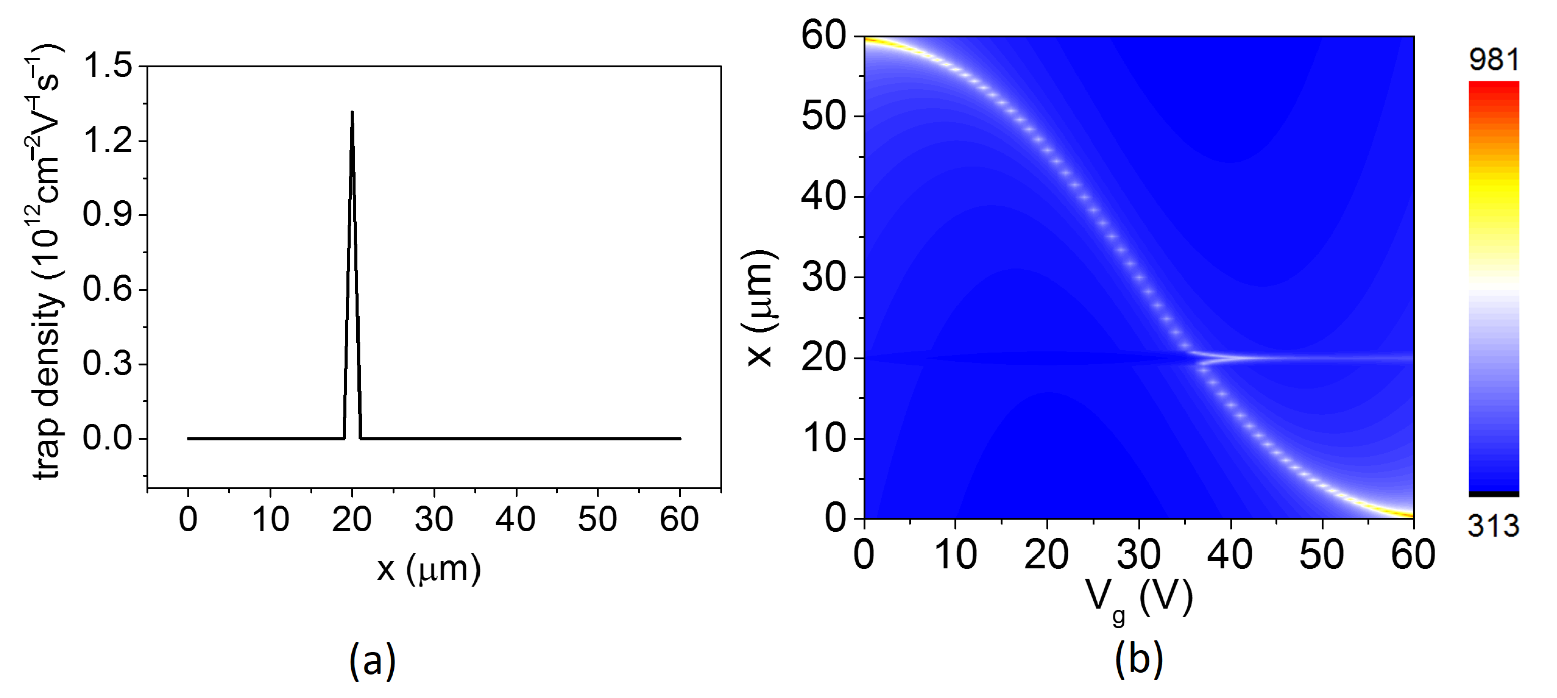
Interestingly, we found that a stationary light spot appeared at a place about 20 m from the drain when extracting the brightest light from Figure 3a, as plotted with blue dots in Figure 3a. This spot almost remained unmoved when changed, which could be caused by locally trapped charges in the oxide that produce image charges in graphene [13]. In view of this, the density carrier equation could be modified by introducing a locally trapped charges function (), as shown in Figure 4a. Then, Equation (6) is rewritten as
The relationship between temperature and gate voltage is calculated using Equations (8), (9) and (11) and plotted in Figure 4b. As we can see, when is beyond 35 V, there are two hot spots on the graphene channel: one could move by increasing the gate voltage, and the other is stuck at the location with trapped positive charges. In fact, it is not enough to describe locally trapped charges by a fixed trapped charges function, because the locally trapped charges in the oxide could be influenced by many factors. Furthermore, the type of locally trapped charges in the oxide is likely to be converted from electron to hole as the changes, so the stationary spot could appear when is lower than 35 V. Regardless, introducing a locally trapped charges function into the density carrier equation is also meaningful to explain the stationary spot at high gate voltages.
4. Conclusions
In summary, we theoretically and experimentally investigated the spatial location of thermal emission in gate-controlled long channel graphene devices. The observed movement of the emission spot and temperature distribution are consistent with those obtained by the theoretical model, confirming that controlling the gate voltage is an effective method to tune the emission location and emission intensity. In addition, the relationship between the carrier density and Fermi level could be deduced by the theoretical model, which is helpful to understand the internal mechanism of graphene emission.
Supplementary Materials
The following supporting information can be downloaded at: https://0-www-mdpi-com.brum.beds.ac.uk/article/10.3390/nano12193457/s1, the detailed derivations and explanation of Equations (1)–(9) of the body text.
Author Contributions
Conceptualization, Y.F., Z.Z. (Zhengzhuo Zhang), Z.Z. (Zhihong Zhu) and C.G.; methodology, J.Z. and X.Y.; software, J.Z. and W.X.; validation, Y.F. and Z.Z. (Zhengzhuo Zhang); formal analysis, J.Z. and W.X.; investigation, Y.F., Z.Z. (Zhengzhuo Zhang) and F.W.; resources, Y.F. and Z.Z. (Zhengzhuo Zhang); data curation, Y.F., Z.Z. (Zhengzhuo Zhang) and F.W.; writing—original draft preparation, Y.F. and Z.Z. (Zhengzhuo Zhang); writing—review and editing, all authors; visualization, Y.F. and Z.Z. (Zhengzhuo Zhang); supervision, C.G. and S.Q.; project administration, Z.Z. (Zhihong Zhu); funding acquisition, S.Q. All authors have read and agreed to the published version of the manuscript.
Funding
This research received no external funding.
Institutional Review Board Statement
Not applicable.
Informed Consent Statement
Not applicable.
Data Availability Statement
Data supporting reported results can be found in Supplementary Materials.
Conflicts of Interest
The authors declare no conflict of interest.
References
- Novoselov, K.S.; Geim, A.K.; Morozov, S.V.; Jiang, D.; Zhang, Y.; Dubonos, S.V.; Grigorieva, I.V.; Firsov, A.A. Electric field effect in atomically thin carbon films. Science 2004, 306, 666–669. [Google Scholar] [CrossRef] [PubMed] [Green Version]
- Bonaccorso, F.; Sun, Z.; Hasan, T.; Ferrari, A.C. Graphene photonics and optoelectronics. Nat. Photonics 2010, 4, 611–622. [Google Scholar] [CrossRef] [Green Version]
- Guo, C.; Zhang, J.; Xu, W.; Liu, K.; Yuan, X.; Qin, S.; Zhu, Z. Graphene-Based Perfect Absorption Structures in the Visible to Terahertz Band and Their Optoelectronics Applications. Nanomaterials 2018, 8, 12. [Google Scholar] [CrossRef] [PubMed] [Green Version]
- Marconcini, P.; Macucci, M. Transport Simulation of Graphene Devices with a Generic Potential in the Presence of an Orthogonal Magnetic Field. Nanomaterials 2022, 12, 1087. [Google Scholar] [CrossRef] [PubMed]
- Castro Neto, A.H.; Guinea, F.; Peres, N.M.R.; Novoselov, K.S.; Geim, A.K. The electronic properties of graphene. Rev. Mod. Phys. 2009, 81, 109–162. [Google Scholar] [CrossRef] [Green Version]
- Kim, Y.D.; Kim, H.; Cho, Y.; Ryoo, J.H.; Park, C.H.; Kim, P.; Kim, Y.S.; Lee, S.; Li, Y.; Park, S.N.; et al. Bright visible light emission from graphene. Nat. Nanotechnol. 2015, 10, 676–681. [Google Scholar] [CrossRef] [PubMed] [Green Version]
- Luo, F.; Fan, Y.; Peng, G.; Xu, S.; Yang, Y.; Yuan, K.; Liu, J.; Ma, W.; Xu, W.; Zhu, Z.H.; et al. Graphene Thermal Emitter with Enhanced Joule Heating and Localized Light Emission in Air. ACS Photonics 2019, 6, 2117–2125. [Google Scholar] [CrossRef]
- Son, S.K.; Šiškins, M.; Mullan, C.; Yin, J.; Kravets, V.G.; Kozikov, A.; Ozdemir, S.; Alhazmi, M.; Holwill, M.; Watanabe, K.; et al. Graphene hot-electron light bulb: Incandescence from hBN-encapsulated graphene in air. 2D Mater. 2017, 5, 011006. [Google Scholar] [CrossRef]
- Engel, M.; Steiner, M.; Lombardo, A.; Ferrari, A.C.; Lohneysen, H.V.; Avouris, P.; Krupke, R. Light-matter interaction in a microcavity-controlled graphene transistor. Nat. Commun. 2012, 3, 906. [Google Scholar] [CrossRef] [PubMed] [Green Version]
- Shiue, R.J.; Gao, Y.; Tan, C.; Peng, C.; Zheng, J.; Efetov, D.K.; Kim, Y.D.; Hone, J.; Englund, D. Thermal radiation control from hot graphene electrons coupled to a photonic crystal nanocavity. Nat. Commun. 2019, 10, 109. [Google Scholar] [CrossRef]
- Shi, C.; Mahlmeister, N.H.; Luxmoore, I.J.; Nash, G.R. Metamaterial-based graphene thermal emitter. Nano Res. 2017, 11, 3567–3573. [Google Scholar] [CrossRef] [Green Version]
- Miyoshi, Y.; Fukazawa, Y.; Amasaka, Y.; Reckmann, R.; Yokoi, T.; Ishida, K.; Kawahara, K.; Ago, H.; Maki, H. High-speed and on-chip graphene blackbody emitters for optical communications by remote heat transfer. Nat. Commun. 2018, 9, 1279. [Google Scholar] [CrossRef] [PubMed] [Green Version]
- Freitag, M.; Chiu, H.Y.; Steiner, M.; Perebeinos, V.; Avouris, P. Thermal infrared emission from biased graphene. Nat. Nanotechnol. 2010, 5, 497–501. [Google Scholar] [CrossRef] [PubMed]
- Tersoff, J.; Freitag, M.; Tsang, J.C.; Avouris, P. Device modeling of long-channel nanotube electro-optical emitter. Appl. Phys. Lett. 2005, 86, 263108. [Google Scholar] [CrossRef] [Green Version]
- Dorgan, V.E.; Behnam, A.; Conley, H.J.; Bolotin, K.I.; Pop, E. High-field electrical and thermal transport in suspended graphene. Nano Lett. 2013, 13, 4581–4586. [Google Scholar] [CrossRef] [Green Version]
- Kathalingam, A.; Senthilkumar, V.; Rhee, J.K. Hysteresis I–V nature of mechanically exfoliated graphene FET. J. Mater. Sci. Mater. Electron. 2014, 25, 1303–1308. [Google Scholar] [CrossRef]
- Joshi, P.; Romero, H.E.; Neal, A.T.; Toutam, V.K.; Tadigadapa, S.A. Intrinsic doping and gate hysteresis in graphene field effect devices fabricated on SiO2 substrates. J. Phys. Condens. Matter. 2010, 22, 334214. [Google Scholar] [CrossRef] [PubMed]
Figure 1.
(a) A schematic of the graphene emitter. The electrical contacts are indicated as source, drain, and gate. (b) The top view of the graphene emitter; the comparison of from theoretical model and simulations for (c) spot position, (d) the maximum temperature, and (e) the current.
Figure 1.
(a) A schematic of the graphene emitter. The electrical contacts are indicated as source, drain, and gate. (b) The top view of the graphene emitter; the comparison of from theoretical model and simulations for (c) spot position, (d) the maximum temperature, and (e) the current.

Figure 2.
(a) The optical micrograph of the graphene thermal emitter with size of 60 m × 5 m; (b) Raman spectrum of the graphene emitter; (c) I-Vg characteristic with at 0.1 V after several annealing in vacuum.
Figure 2.
(a) The optical micrograph of the graphene thermal emitter with size of 60 m × 5 m; (b) Raman spectrum of the graphene emitter; (c) I-Vg characteristic with at 0.1 V after several annealing in vacuum.

Figure 3.
(a) Spatial images of the integrated infrared emission (with wavelength in the range from 950 nm to 1700 nm) of the graphene emitter with Vd of 70 V at different gate voltages; (b) the relationship between emission spots and the gate voltage; (c) the temperatures of movable spots and (d) the current dependent on the gate voltage.

Figure 4.
(a) The trapped charges as a function of position; (b) the temperature distribution with respect to the and position.
Figure 4.
(a) The trapped charges as a function of position; (b) the temperature distribution with respect to the and position.

Publisher’s Note: MDPI stays neutral with regard to jurisdictional claims in published maps and institutional affiliations. |
© 2022 by the authors. Licensee MDPI, Basel, Switzerland. This article is an open access article distributed under the terms and conditions of the Creative Commons Attribution (CC BY) license (https://creativecommons.org/licenses/by/4.0/).
Share and Cite
MDPI and ACS Style
Fan, Y.; Zhang, Z.; Zhu, Z.; Zhang, J.; Xu, W.; Wu, F.; Yuan, X.; Guo, C.; Qin, S. Regulation of Thermal Emission Position in Biased Graphene. Nanomaterials 2022, 12, 3457. https://0-doi-org.brum.beds.ac.uk/10.3390/nano12193457
AMA Style
Fan Y, Zhang Z, Zhu Z, Zhang J, Xu W, Wu F, Yuan X, Guo C, Qin S. Regulation of Thermal Emission Position in Biased Graphene. Nanomaterials. 2022; 12(19):3457. https://0-doi-org.brum.beds.ac.uk/10.3390/nano12193457
Chicago/Turabian StyleFan, Yansong, Zhengzhuo Zhang, Zhihong Zhu, Jianfa Zhang, Wei Xu, Fan Wu, Xiaodong Yuan, Chucai Guo, and Shiqiao Qin. 2022. "Regulation of Thermal Emission Position in Biased Graphene" Nanomaterials 12, no. 19: 3457. https://0-doi-org.brum.beds.ac.uk/10.3390/nano12193457
Note that from the first issue of 2016, this journal uses article numbers instead of page numbers. See further details here.