
Defect-Rich Monolayer MoS2 as a Universally Enhanced Substrate for Surface-Enhanced Raman Scattering

 , , , and
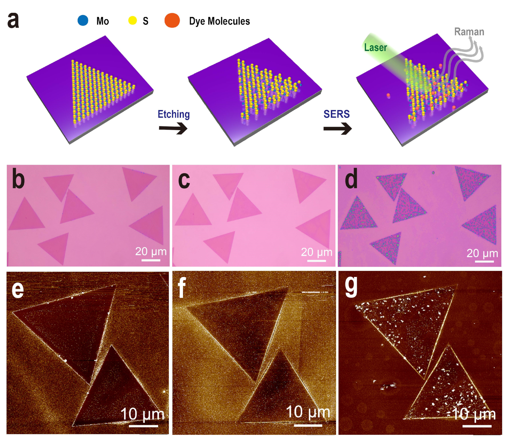
Abstract
:1. Introduction
2. Materials and Methods
2.1. Synthesis of Monolayer MoS2
2.2. Synthesis of Etched MoS2
2.3. Materials Characterization
2.4. SERS Measurements
2.5. DFT Calculation Details
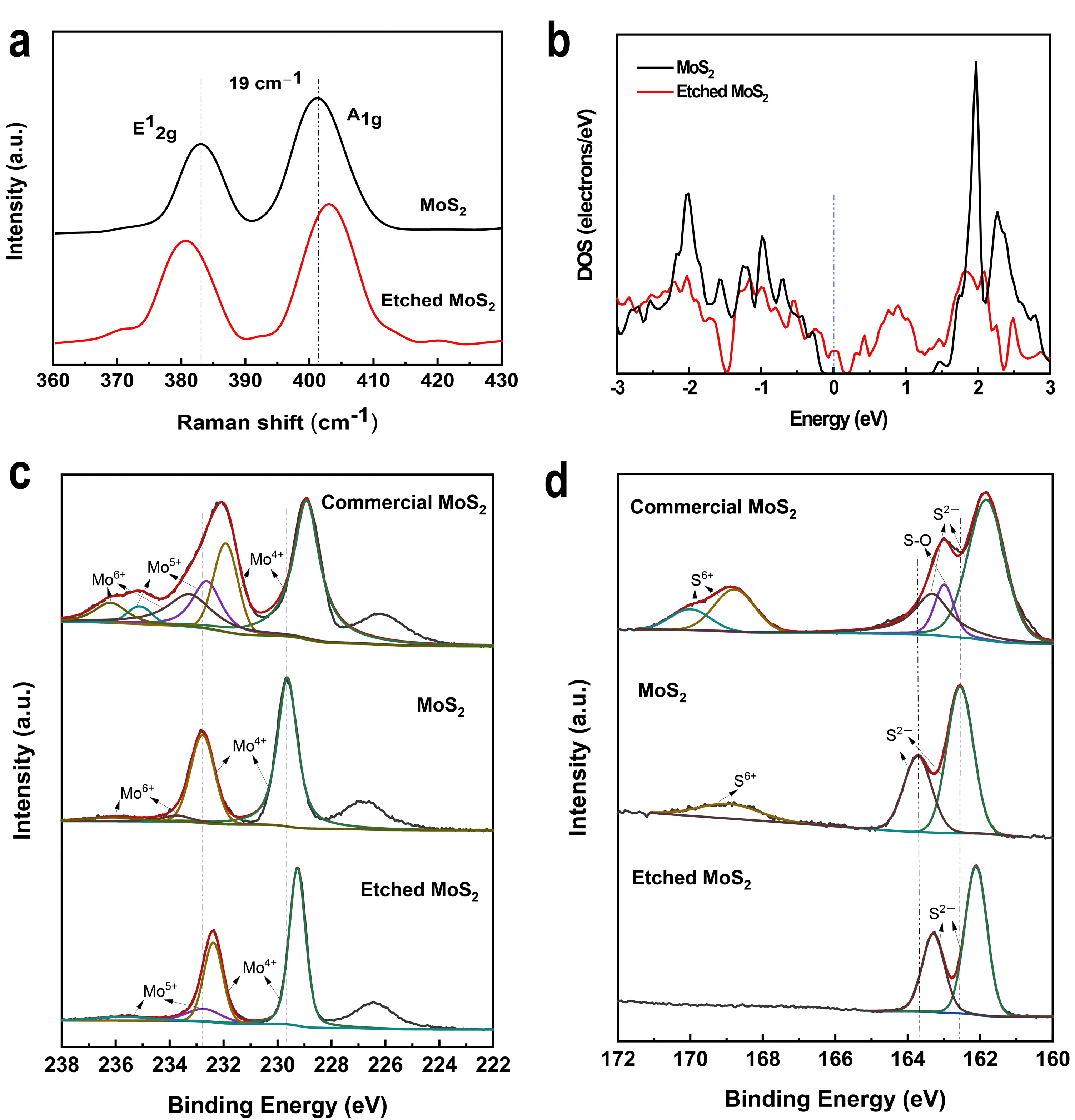
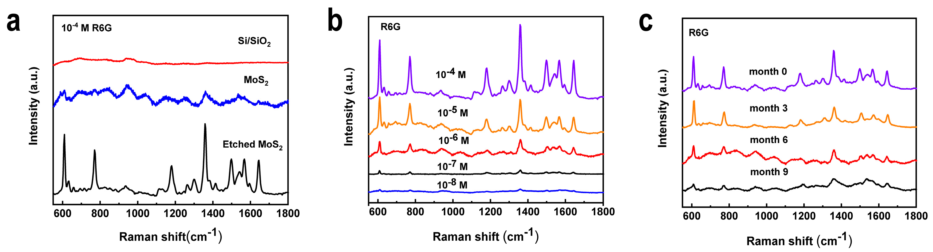
3. Results and Discussion
4. Conclusions
Supplementary Materials
Author Contributions
Funding
Institutional Review Board Statement
Informed Consent Statement
Data Availability Statement
Conflicts of Interest
References
- Wang, Y.; Iglesias, D.; Gali, S.M.; Beljonne, D.; Samorì, P. Light-Programmable Logic-in-Memory in 2D Semiconductors Enabled by Supramolecular Functionalization: Photoresponsive Collective Effect of Aligned Molecular Dipoles. ACS Nano 2021, 15, 13732–13741. [Google Scholar] [CrossRef] [PubMed]
- Wang, Y.; Gali, S.M.; Slassi, A.; Beljonne, D.; Samorì, P. Collective Dipole-Dominated Doping of Monolayer MoS2: Orientation and Magnitude Control via the Supramolecular Approach. Adv. Funct. Mater. 2020, 30, 2002846. [Google Scholar] [CrossRef]
- Qiu, H.; Liu, Z.; Yao, Y.; Herder, M.; Hecht, S.; Samorì, P. Simultaneous Optical Tuning of Hole and Electron Transport in Ambipolar WSe2 Interfaced with a Bicomponent Photochromic Layer: From High-Mobility Transistors to Flexible Multilevel Memories. Adv. Mater. 2020, 32, 1907903. [Google Scholar] [CrossRef]
- Calavalle, F.; Dreher, P.; Surdendran, A.P.; Wan, W.; Timpel, M.; Verucchi, R.; Rogero, C.; Bauch, T.; Lombardi, F.; Casanova, F.; et al. Tailoring Superconductivity in Large-Area Single-Layer NbSe2 via Self-Assembled Molecular Adlayers. Nano Lett. 2021, 21, 136–143. [Google Scholar] [CrossRef] [PubMed]
- Xu, G.; Wang, X.; Sun, Y.; Chen, X.; Zheng, J.; Sun, L.; Jiao, L.; Li, J. Metallic and ferromagnetic MoS2 nanobelts with vertically aligned edges. Nano Res. 2015, 8, 2946–2953. [Google Scholar] [CrossRef]
- Chen, M.; Liu, D.; Du, X.; Lo, K.H.; Wang, S.; Zhou, B.; Pan, H. 2D materials: Excellent substrates for surface-enhanced Raman scattering (SERS) in chemical sensing and biosensing. Trends Anal. Chem. 2020, 130, 115983. [Google Scholar] [CrossRef]
- Nie, S.; Emory, S.R. Probing Single Molecules and Single Nanoparticles by Surface-Enhanced Raman Scattering. Science 1997, 275, 1102–1106. [Google Scholar] [CrossRef]
- Schlücker, S. Surface-Enhanced Raman Spectroscopy: Concepts and Chemical Applications. Angew. Chem. Int. Ed. 2014, 53, 4756–4795. [Google Scholar] [CrossRef]
- Tao, L.; Chen, K.; Chen, Z.; Cong, C.; Qiu, C.; Chen, J.; Wang, X.; Chen, H.; Yu, T.; Xie, W.; et al. 1T′ Transition Metal Telluride Atomic Layers for Plasmon-Free SERS at Femtomolar Levels. J. Am. Chem. Soc. 2018, 140, 8696–8704. [Google Scholar] [CrossRef]
- Langer, J.; de Aberasturi, D.J.; Aizpurua, J.; Alvarez-Puebla, R.A.; Auguié, B.; Baumberg, J.J.; Bazan, G.C.; Bell, S.E.J.; Boisen, A.; Brolo, A.G.; et al. Present and Future of Surface-Enhanced Raman Scattering. ACS Nano 2020, 14, 28–117. [Google Scholar] [CrossRef] [Green Version]
- Liu, R.; Jiang, L.; Yu, Z.; Jing, X.; Liang, X.; Wang, D.; Yang, B.; Lu, C.; Zhou, W.; Jin, S. MXene (Ti3C2Tx)-Ag nanocomplex as efficient and quantitative SERS biosensor platform by in-situ PDDA electrostatic self-assembly synthesis strategy. Sens. Actuators B Chem. 2021, 333, 129581. [Google Scholar] [CrossRef]
- Yu, J.; Yang, M.; Li, Z.; Liu, C.; Wei, Y.; Zhang, C.; Man, B.; Lei, F. Hierarchical Particle-In-Quasicavity Architecture for Ultratrace In Situ Raman Sensing and Its Application in Real-Time Monitoring of Toxic Pollutants. Anal. Chem. 2020, 92, 14754–14761. [Google Scholar] [CrossRef] [PubMed]
- Song, X.; Yi, W.; Li, J.; Kong, Q.; Bai, H.; Xi, G. Selective Preparation of Mo2N and MoN with High Surface Area for Flexible SERS Sensing. Nano Lett. 2021, 21, 4410–4414. [Google Scholar] [CrossRef] [PubMed]
- Bell, S.E.J.; Charron, G.; Cortés, E.; Kneipp, J.; de la Chapelle, M.L.; Langer, J.; Procházka, M.; Tran, V.; Schlücker, S. Towards Reliable and Quantitative Surface-Enhanced Raman Scattering (SERS): From Key Parameters to Good Analytical Practice. Angew. Chem. Int. Ed. 2020, 59, 5454–5462. [Google Scholar] [CrossRef] [Green Version]
- Liang, X.; Li, N.; Zhang, R.; Yin, P.; Zhang, C.; Yang, N.; Liang, K.; Kong, B. Carbon-based SERS biosensor: From substrate design to sensing and bioapplication. NPG Asia Mater. 2021, 13, 8. [Google Scholar] [CrossRef]
- Zhao, X.; Liu, C.; Yu, J.; Li, Z.; Liu, L.; Li, C.; Xu, S.; Li, W.; Man, B.; Zhang, C. Hydrophobic multiscale cavities for high-performance and self-cleaning surface-enhanced Raman spectroscopy (SERS) sensing. Nanophotonics 2020, 9, 4761–4773. [Google Scholar] [CrossRef]
- Song, G.; Gong, W.; Cong, S.; Zhao, Z. Ultrathin Two-Dimensional Nanostructures: Surface Defects for Morphology-Driven Enhanced Semiconductor SERS. Angew. Chem. Int. Ed. 2021, 60, 5505–5511. [Google Scholar] [CrossRef]
- Wang, X.; Shi, W.; Jin, Z.; Huang, W.; Lin, J.; Ma, G.; Li, S.; Guo, L. Remarkable SERS Activity Observed from Amorphous ZnO Nanocages. Angew. Chem. Int. Ed. 2017, 56, 9851–9855. [Google Scholar] [CrossRef]
- Rani, R.; Yoshimura, A.; Das, S.; Sahoo, M.R.; Kundu, A.; Sahu, K.K.; Meunier, V.; Nayak, S.K.; Koratkar, N.; Hazra, K.S. Sculpting Artificial Edges in Monolayer MoS2 for Controlled Formation of Surface-Enhanced Raman Hotspots. ACS Nano 2020, 14, 6258–6268. [Google Scholar] [CrossRef]
- Chen, L.-Y.; Yu, J.-S.; Fujita, T.; Chen, M.-W. Nanoporous Copper with Tunable Nanoporosity for SERS Applications. Adv. Funct. Mater. 2009, 19, 1221–1226. [Google Scholar] [CrossRef]
- Si, S.; Liang, W.; Sun, Y.; Huang, J.; Ma, W.; Liang, Z.; Bao, Q.; Jiang, L. Facile Fabrication of High-Density Sub-1-nm Gaps from Au Nanoparticle Monolayers as Reproducible SERS Substrates. Adv. Funct. Mater. 2016, 26, 8137–8145. [Google Scholar] [CrossRef]
- Huo, D.; Chen, B.; Meng, G.; Huang, Z.; Li, M.; Lei, Y. Ag-Nanoparticles@Bacterial Nanocellulose as a 3D Flexible and Robust Surface-Enhanced Raman Scattering Substrate. ACS Appl. Mater. Interfaces 2020, 12, 50713–50720. [Google Scholar] [CrossRef] [PubMed]
- Sun, G.; Li, N.; Wang, D.; Xu, G.; Zhang, X.; Gong, H.; Li, D.; Li, Y.; Pang, H.; Gao, M.; et al. A Novel 3D Hierarchical Plasmonic Functional Cu@Co3O4@Ag Array as Intelligent SERS Sensing Platform with Trace Droplet Rapid Detection Ability for Pesticide Residue Detection on Fruits and Vegetables. Nanomaterials 2021, 11, 3460. [Google Scholar] [CrossRef] [PubMed]
- Zhang, C.; Li, C.; Yu, J.; Jiang, S.; Xu, S.; Yang, C.; Liu, Y.J.; Gao, X.; Liu, A.; Man, B. SERS activated platform with three-dimensional hot spots and tunable nanometer gap. Sens. Actuators B Chem. 2018, 258, 163–171. [Google Scholar] [CrossRef]
- Brill, A.R.; Biswas, S.; Caspary Toroker, M.; de Ruiter, G.; Koren, E. Dipole-Induced Raman Enhancement Using Noncovalent Azobenzene-Functionalized Self-Assembled Monolayers on Graphene Terraces. ACS Appl. Mater. Interfaces 2021, 13, 10271–10278. [Google Scholar] [CrossRef]
- Gong, H.; Zheng, X.; Zeng, K.; Yang, B.; Liang, X.; Li, L.; Tao, Y.; Yang, R. Ni3Fe nanoalloys embedded in N-doped carbon derived from dual-metal ZIF: Efficient bifunctional electrocatalyst for Zn-air battery. Carbon 2021, 174, 475–483. [Google Scholar] [CrossRef]
- Ling, X.; Fang, W.; Lee, Y.-H.; Araujo, P.T.; Zhang, X.; Rodriguez-Nieva, J.F.; Lin, Y.; Zhang, J.; Kong, J.; Dresselhaus, M.S. Raman Enhancement Effect on Two-Dimensional Layered Materials: Graphene, h-BN and MoS2. Nano Lett. 2014, 14, 3033–3040. [Google Scholar] [CrossRef]
- Zhao, S.; Wang, H.; Niu, L.; Xiong, W.; Chen, Y.; Zeng, M.; Yuan, S.; Fu, L. 2D GaN for Highly Reproducible Surface Enhanced Raman Scattering. Small 2021, 17, 2103442. [Google Scholar] [CrossRef]
- Muehlethaler, C.; Considine, C.R.; Menon, V.; Lin, W.C.; Lee, Y.H.; Lombardi, J.R.J.A.P. Ultrahigh Raman Enhancement on Monolayer MoS2. ACS Photonics 2016, 3, 1164–1169. [Google Scholar] [CrossRef]
- Cong, S.; Yuan, Y.; Chen, Z.; Hou, J.; Yang, M.; Su, Y.; Zhang, Y.; Li, L.; Li, Q.; Geng, F.; et al. Noble metal-comparable SERS enhancement from semiconducting metal oxides by making oxygen vacancies. Nat. Commun. 2015, 6, 7800. [Google Scholar] [CrossRef]
- Lombardi, J.R.; Birke, R.L. Theory of Surface-Enhanced Raman Scattering in Semiconductors. J. Phys. Chem. C 2014, 118, 11120–11130. [Google Scholar] [CrossRef]
- Zheng, Z.; Cong, S.; Gong, W.; Xuan, J.; Li, G.; Lu, W.; Geng, F.; Zhao, Z. Semiconductor SERS enhancement enabled by oxygen incorporation. Nat. Commun. 2017, 8, 1993. [Google Scholar] [CrossRef] [Green Version]
- Li, Y.; Wang, D.; Xu, G.; Qiao, L.; Li, Y.; Gong, H.; Shi, L.; Li, D.; Gao, M.; Liu, G.; et al. ZIF-8/PI Nanofibrous Membranes With High-Temperature Resistance for Highly Efficient PM0.3 Air Filtration and Oil-Water Separation. Front. Chem. 2021, 9, 810861. [Google Scholar] [CrossRef] [PubMed]
- Wang, X.; Shi, W.; Wang, S.; Zhao, H.; Lin, J.; Yang, Z.; Chen, M.; Guo, L. Two-Dimensional Amorphous TiO2 Nanosheets Enabling High-Efficiency Photoinduced Charge Transfer for Excellent SERS Activity. J. Am. Chem. Soc. 2019, 141, 5856–5862. [Google Scholar] [CrossRef] [PubMed]
- Yin, Y.; Miao, P.; Zhang, Y.; Han, J.; Zhang, X.; Gong, Y.; Gu, L.; Xu, C.; Yao, T.; Xu, P.; et al. Significantly Increased Raman Enhancement on MoX2 (X = S, Se) Monolayers upon Phase Transition. Adv. Funct. Mater. 2017, 27, 1606694. [Google Scholar] [CrossRef]
- Sun, L.; Hu, H.; Zhan, D.; Yan, J.; Liu, L.; Teguh, J.S.; Yeow, E.K.L.; Lee, P.S.; Shen, Z. Plasma Modified MoS2 Nanoflakes for Surface Enhanced Raman Scattering. Small 2014, 10, 1090–1095. [Google Scholar] [CrossRef]
- Qiu, H.; Li, Z.; Gao, S.; Chen, P.; Li, H.J.R.A. Large-Area MoS2 Thin layers Directly Synthesized on Pyramid-Si Substrate for Surface-Enhanced Raman Scattering. RSC Adv. 2015, 5, 83899–83905. [Google Scholar] [CrossRef]
- Ippolito, S.; Kelly, A.G.; Furlan de Oliveira, R.; Stoeckel, M.-A.; Iglesias, D.; Roy, A.; Downing, C.; Bian, Z.; Lombardi, L.; Samad, Y.A.; et al. Covalently interconnected transition metal dichalcogenide networks via defect engineering for high-performance electronic devices. Nat. Nanotechnol. 2021, 16, 592–598. [Google Scholar] [CrossRef]
- Wang, S.; Lee, G.-D.; Lee, S.; Yoon, E.; Warner, J.H. Detailed Atomic Reconstruction of Extended Line Defects in Monolayer MoS2. ACS Nano 2016, 10, 5419–5430. [Google Scholar] [CrossRef]
- Zheng, J.; Du, H.; Jiang, F.; Zhang, Z.; Sa, B.; He, W.; Jiao, L.; Zhan, H. Rapid and Large-Scale Quality Assessment of Two-Dimensional MoS2 Using Sulfur Particles with Optical Visualization. Nano Lett. 2021, 21, 1260–1266. [Google Scholar] [CrossRef]
- Zheng, J.; Yan, X.; Lu, Z.; Qiu, H.; Xu, G.; Zhou, X.; Wang, P.; Pan, X.; Liu, K.; Jiao, L. High-Mobility Multilayered MoS2 Flakes with Low Contact Resistance Grown by Chemical Vapor Deposition. Adv. Mater. 2017, 29, 1604540. [Google Scholar] [CrossRef] [PubMed]
- Sun, R.; Sun, S.; Liang, X.; Gong, H.; Zhang, X.; Li, Y.; Gao, M.; Li, D.; Xu, G. Surface Charge Transfer Doping of MoS2 Monolayer by Molecules with Aggregation-Induced Emission Effect. Nanomaterials 2022, 12, 164. [Google Scholar] [CrossRef] [PubMed]
- Kresse, G.; Joubert, D. From ultrasoft pseudopotentials to the projector augmented-wave method. Phys. Rev. B 1999, 59, 1758–1775. [Google Scholar] [CrossRef]
- Perdew, J.P.; Burke, K.; Ernzerhof, M. Generalized Gradient Approximation Made Simple. Phys. Rev. Lett. 1996, 77, 3865–3868. [Google Scholar] [CrossRef] [PubMed] [Green Version]
- Sun, L.; Yan, X.; Zheng, J.; Yu, H.; Lu, Z.; Gao, S.-p.; Liu, L.; Pan, X.; Wang, D.; Wang, Z.; et al. Layer-Dependent Chemically Induced Phase Transition of Two-Dimensional MoS2. Nano Lett. 2018, 18, 3435–3440. [Google Scholar] [CrossRef] [PubMed]
- Lombardi, J.R.; Birke, R.L. A Unified Approach to Surface-Enhanced Raman Spectroscopy. J. Phys. Chem. C 2008, 112, 5605–5617. [Google Scholar] [CrossRef]
- Jensen, L.; Schatz, G.C. Resonance Raman Scattering of Rhodamine 6G as Calculated Using Time-Dependent Density Functional Theory. J. Phys. Chem. A 2006, 110, 5973–5977. [Google Scholar] [CrossRef]


Publisher’s Note: MDPI stays neutral with regard to jurisdictional claims in published maps and institutional affiliations. |
© 2022 by the authors. Licensee MDPI, Basel, Switzerland. This article is an open access article distributed under the terms and conditions of the Creative Commons Attribution (CC BY) license (https://creativecommons.org/licenses/by/4.0/).
Share and Cite
Sun, S.; Zheng, J.; Sun, R.; Wang, D.; Sun, G.; Zhang, X.; Gong, H.; Li, Y.; Gao, M.; Li, D.; et al. Defect-Rich Monolayer MoS2 as a Universally Enhanced Substrate for Surface-Enhanced Raman Scattering. Nanomaterials 2022, 12, 896. https://0-doi-org.brum.beds.ac.uk/10.3390/nano12060896
Sun S, Zheng J, Sun R, Wang D, Sun G, Zhang X, Gong H, Li Y, Gao M, Li D, et al. Defect-Rich Monolayer MoS2 as a Universally Enhanced Substrate for Surface-Enhanced Raman Scattering. Nanomaterials. 2022; 12(6):896. https://0-doi-org.brum.beds.ac.uk/10.3390/nano12060896
Chicago/Turabian StyleSun, Shiyu, Jingying Zheng, Ruihao Sun, Dan Wang, Guanliang Sun, Xingshuang Zhang, Hongyu Gong, Yong Li, Meng Gao, Dongwei Li, and et al. 2022. "Defect-Rich Monolayer MoS2 as a Universally Enhanced Substrate for Surface-Enhanced Raman Scattering" Nanomaterials 12, no. 6: 896. https://0-doi-org.brum.beds.ac.uk/10.3390/nano12060896