
A Study to Improve the Performance of Mixed Cation–Halide Perovskite-Based UVC Photodetectors


Department of Electrical Engineering, Gachon University, 1342 Seongnam-daero, Seongnam-si 13120, Korea
*
Author to whom correspondence should be addressed.
Nanomaterials 2022, 12(7), 1132; https://0-doi-org.brum.beds.ac.uk/10.3390/nano12071132
Submission received: 28 February 2022
/
Revised: 25 March 2022
/
Accepted: 26 March 2022
/
Published: 29 March 2022
(This article belongs to the Special Issue Nanogenerator for Self-Powering Indoor Electronics)
Abstract
:Photodetectors convert optical signals into electrical signals and demonstrate application potential in various fields, such as optical communication, image detection, environmental monitoring, and optoelectronics. In this study, a mixed cation–halide perovskite-based ultraviolet C photodetector was fabricated using a solution process. The higher the mobility of the perovskite carrier, which is one of the factors affecting the performance of electronic power devices, the better the carrier diffusion. The on/off ratio and responsivity indicate the sensitivity of the response, and together with the detectivity and external quantum efficiency, these parameters demonstrate the performance of the detector. The detector fabricated in this study exhibited a mobility of 202.2 cm2/Vs and a high on/off ratio of 105% at a −2 V bias, under 254 nm light irradiation with an intensity of 0.6 mW/cm2. The responsivity, detectivity, and external quantum efficiency of the as-fabricated detector were 5.07 mA/W, 5.49 × 10¹¹ Jones, and 24.8%, respectively. These findings demonstrate that the solution process employed in this study is suitable for the fabrication of mixed cation–halide perovskites which show immense potential for use as photodetectors.
1. Introduction
A photodetector is a device that converts an optical signal into an electrical signal and exhibits a high detection rate, allowing the detection of weak optical signals [1,2]. Photodetectors have been used in various fields, such as optical communication, image detection, and environmental monitoring [3,4,5,6]. In particular, ultraviolet C (UVC) photodetectors operating in the 280–100 nm region have been intensively studied owing to their ability to precisely detect weak signals [7]. UV rays can be divided into three categories according to wavelength: UVA (400–320 nm), UVB (320–280 nm), and UVC (280–100 nm) [8]. UVC radiation is largely absorbed by the ozone layer [8]. However, UVC radiation is emitted by artificial light sources, such as mercury lamps, UV germicidal bulbs, and arc discharges [9,10,11,12], and is harmful to human health. Additionally, it is the cause of many safety issues in industrial facilities [13,14]. Therefore, it is essential to develop a system to detect UVC radiation in order to increase worker safety and reduce facility management costs.
When fabricating a UVC photodetector, it is necessary to consider whether a low-temperature and simple process is possible. This is because it is essential to develop sustainable electronic devices to reduce the impacts on the environment of energy consumption and waste [15,16]. Low energy processes make it possible to produce more eco-friendly devices [17].
Various characteristics of photodetectors, such as stability, light absorption, carrier mobility, band gap, reactivity, detectability, and on/off ratio, are dependent on the material composition. Accordingly, photodetectors comprising various materials have been investigated [1]. Photodetectors comprising materials such as group III–V compound semiconductors, organic polymers, and silicon have been fabricated [2], and narrow bandgap Si diode sensors equipped with UV filters have been developed [14]. However, photodetectors containing these materials are expensive and require complex fabrication processes [18]. Additionally, Si diodes offer limited UVC sensitivity because the photogenerated carriers cannot easily reach the depletion layer of the semiconductor [14].
Recently, perovskites have attracted attention in the field of optoelectronic devices, such as light-emitting diodes and solar cells [19,20], owing to their tunable bandgaps, large light absorption, and long diffusion lengths (LD values) [21]. In addition, the solution process fabrication of perovskites is simple and economical [22,23].
Methylammonium (MA) and formamidinium (FA) cations are commonly used in perovskite light absorption layers [21,24], and methylammonium lead halide (MAPbX3) has attracted attention as a material for developing hybrid organic–inorganic perovskites owing to its excellent photoelectric properties [25]. However, MAPbX3 perovskites exhibit phase instability at high temperatures and are more sensitive to moisture and light than FA-based perovskites, leading to the separation of halide components [26,27]. Formamidinium lead halides (FAPbX3) have a higher thermal stability than MAPbX3 [24,28]; however, FAPbI3 exhibits low phase stability at room temperature and can be converted from the “black” α-phase to the “yellow” δ-phase [29,30].
Therefore, perovskite materials comprising only pure cation MA or FA are not optimal owing to their instability. However, the incorporation of MA+ into FAPbI3-based perovskite via the crystal nucleation mechanism prevents the formation of δ-FAPbI3 [31], and this stabilization improves performance [32]. Additionally, the iodide can be partially substituted with a bromide to improve the performance of FA/MA mixed cation perovskites, as the addition of a small amount of Br− improves phase stability [33,34]. The partial substitution of I− with Br− maintains excellent light absorption properties and increases the carrier lifetime and mobility [25]. The mixed cation–halide perovskite features improvements in crystallinity, stability, and electrical properties, such as light absorption, photocurrent, carrier mobility, and LD. Therefore, mixed cation–halide perovskites have potential as materials for use in high performance UVC photodetectors with a low energy process and cost.
In this study, (FAPbI3)1−x(MAPbBr3)x (x = 0, 0.03, 0.05, 0.07, and 0.1) photodetectors were fabricated by adding MAPbBr3 to FAPbI3, considering the low thermal stability of MABr at different mol% ratios. The fabricated mixed cation–halide perovskite-based photodetector exhibited improved stability, photocurrent, and responsiveness compared with a pure FAPbI3 photodetector. The performance of the photodetector was determined by investigating various characteristics, including responsivity, detectivity, carrier mobility, light absorption, dark environment, and current under 254 nm irradiation. The responsivity, detectivity, and external quantum efficiency (EQE) of the as-fabricated (FAPbI3)1−x(MAPbBr3)x-based photodetectors were 5.07 mA/W, 5.49 × 10¹¹ Jones, and 24.8%, respectively, under 254 nm light irradiation with a −2 V bias and 0.6 mW/cm2 intensity. This value is more than six times larger than that of a pure FAPbI3 photodetector. These results show that the mixed cation–halide perovskite provides improved optical properties compared with the pure FAPbI3 perovskite, and therefore, is a promising candidate for UVC photodetector fabrication.
2. Materials and Methods
2.1. Materials
The materials and chemicals used were as follows: quartz indium tin oxide (ITO) patterned glass (etching interval: 10 μm) with a thickness of 150 nm, lead (II) iodide (99.999% trace metal basis), N,N-dimethylformamide (DMF, 99.8%), toluene (99.8%), dimethyl sulfoxide (DMSO, 99.7%), FA iodide (FAI), MA iodide (MAI), and MA chloride (MACl).
2.2. Preparation of (FAPbI3)1−x(MAPbBr3)x-Based Perovskite Photodetector
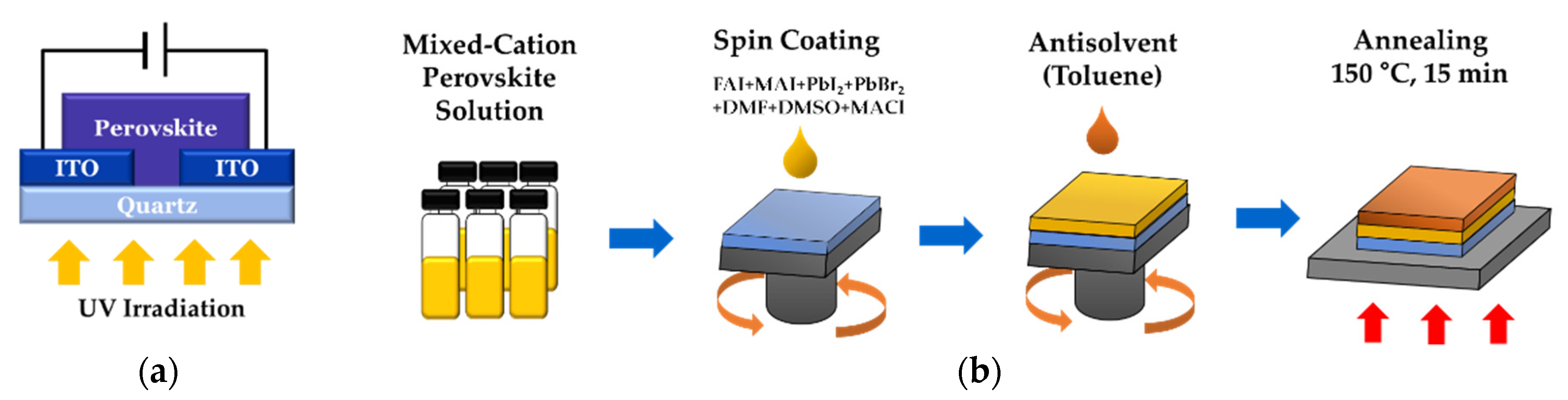
Figure 1a shows a schematic diagram of a metal-semiconductor-metal-type photodetector, and Figure 1b illustrates the fabrication process. An ITO quartz substrate etched at 10 µm intervals was used to prepare the (FAPbI3)1−x(MAPbBr3)x films. To remove organic matter, the ITO quartz substrate was ultrasonically cleaned using a neutral detergent, water, acetone, ethanol, and distilled water for 20 min each. After drying in an oven at 80 °C for 20 min, UV-ozone treatment was performed for 30 min to further remove moisture. A (FAPbI3)1−x(MAPbBr3)x solution was prepared by dissolving PbI2 and PbBr2 (1.4 M), FAI, and MABr (1.4 M) in DMF (1 mL), which was then mixed with 100 µL of DMSO. The perovskite precursor solution was then stirred for 1 h at 23 °C. MACl was then added, up to 40 mol% of FAI, and the solution was further stirred for 30 min. The solution was deposited on a quartz substrate via spin coating at 4000 rpm for 20 s, over which toluene was dropped for the last 10 s. After spin-coating, the thin film was annealed at 150 °C for 15 min.
2.3. Device Characterization
The crystal structure of the perovskite film was investigated using X-ray diffraction (XRD, DMAX 2200, Rigaku, Japan) with a scan rate of 3.00°/min. The morphology of the photodetector surface was observed using scanning electron microscopy (SEM, S-4700, Hitachi, Japan). The light absorptivity of the device was measured using UV-visible (UV-vis) spectroscopy (UV-vis 8453, Agilent, Santa Clara, CA, USA). The electrical response of the perovskite photodetector was measured with a combined source and measurement meter (Source Measure Unit, Keithley Instruments, Cleveland, OH, USA) and a UV lamp (6 W, 254 nm) (VL-6.LC, Vilber Lourmat, Marne-la-Vallée, France) under 254 nm irradiation.
3. Results and Discussion
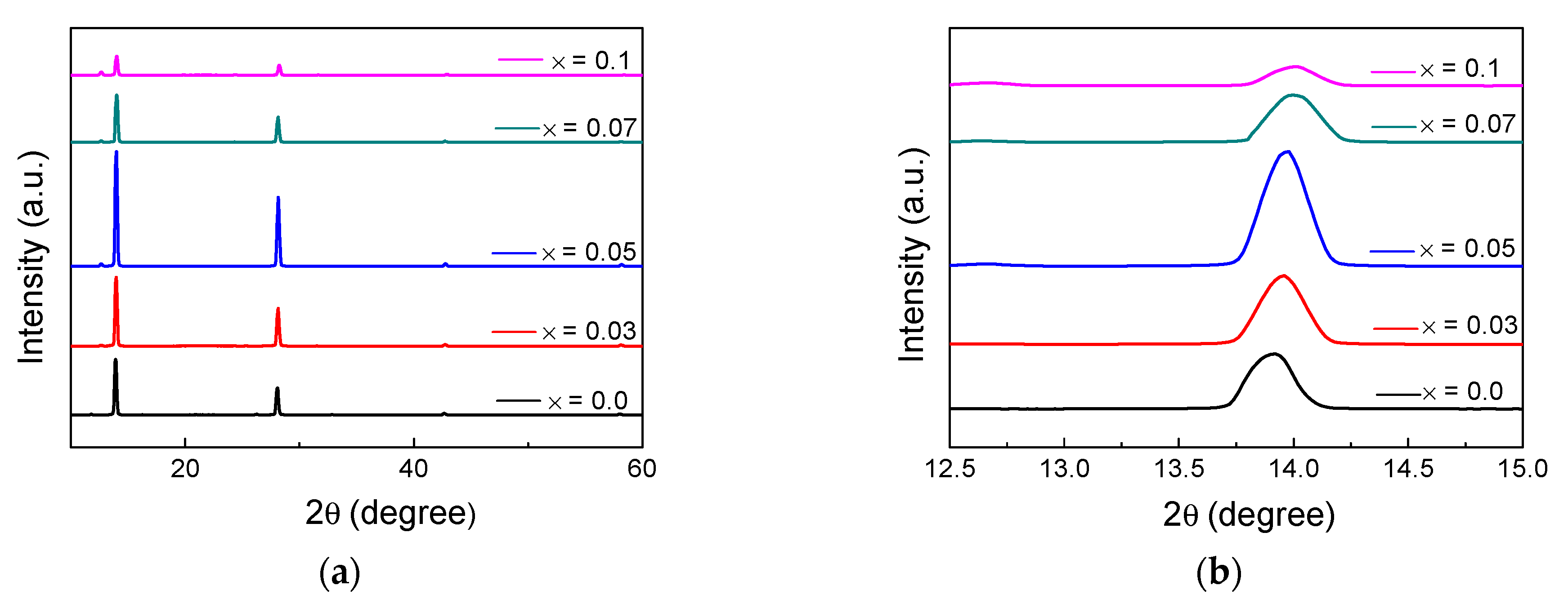
Figure 2a shows the XRD patterns of the fabricated perovskites. (FAPbI3)1−x(MAPbBr3)x films were fabricated with different ratios of x (x = 0, 0.03, 0.05, 0.07, and 0.1). Several characteristic perovskite peaks were observed in the XRD patterns. The peaks at ~11.7°, ~12.7°, and ~14.0° of the diffractogram were assigned to the δ-FAPbI3, PbI2, and α-FAPbI3 phases, respectively. Pure FAPbI3 (x = 0) exhibited the highest δ-FAPbI3 peak intensity and possessed low phase stability owing to the high concentration of δ-FAPbI3. As the MAPbBr3 content of the film increased, δ-FAPbI3 was converted to α-FAPbI3 [25], which decreased the peak intensity of δ-FAPbI3. However, the reduction of the δ-FAPbI3 content did not improve the crystallinity of the all perovskite films. Although the α-FAPbI3 peak intensity of the (FAPbI3)1−x(MAPbBr3)x film increased up to x = 0.05, it started to decrease at x = 0.07 and exhibited the smallest peak intensity at x = 0.1. This is because the low thermal stability of MABr led to the degradation of MAPbBr3. As the “black” α-FAPbI3 phase is thermodynamically stable above 150 °C, FAPbI3 was annealed at 150 °C [32]. However, MA+ has low thermal stability [26], and therefore, at high temperatures, a portion of MAPbBr3 thermally decomposes to form a PbI2 phase [32,35]. The highest PbI2 peak intensity was observed when x = 0.1, as shown in Figure 2a.
Figure 2b shows that as the content of (MAPbBr3)x increased, the peak shifted to a high diffraction angle. This shows that the perovskite films were successfully formed, as lattice shrinkage is expected to occur when FA+ (2.79 Å) is replaced with MA+ (2.70 Å) [35]. Moreover, additional lattice shrinkage is expected when Br− (1.96 Å) replaces I− (2.2 Å), which shifts the corresponding peak to high diffraction angles [32,36].
The results shown in Figure 2 demonstrate that when mixed cation–halide perovskites were prepared, the content of δ-FAPbI3 decreased compared to that of the pure FAPbI3, and the phase stability improved. In particular, the crystallinity of (FAPbI3)0.95(MAPbBr3)0.05 was the highest among the synthesized samples. However, when more than 7 mol% MAPbBr3 was added, a decrease in crystallinity, owing to the formation of a residue, was observed. This indicates that the overall crystallinity varies depending on the composition of the mixed cation perovskite.
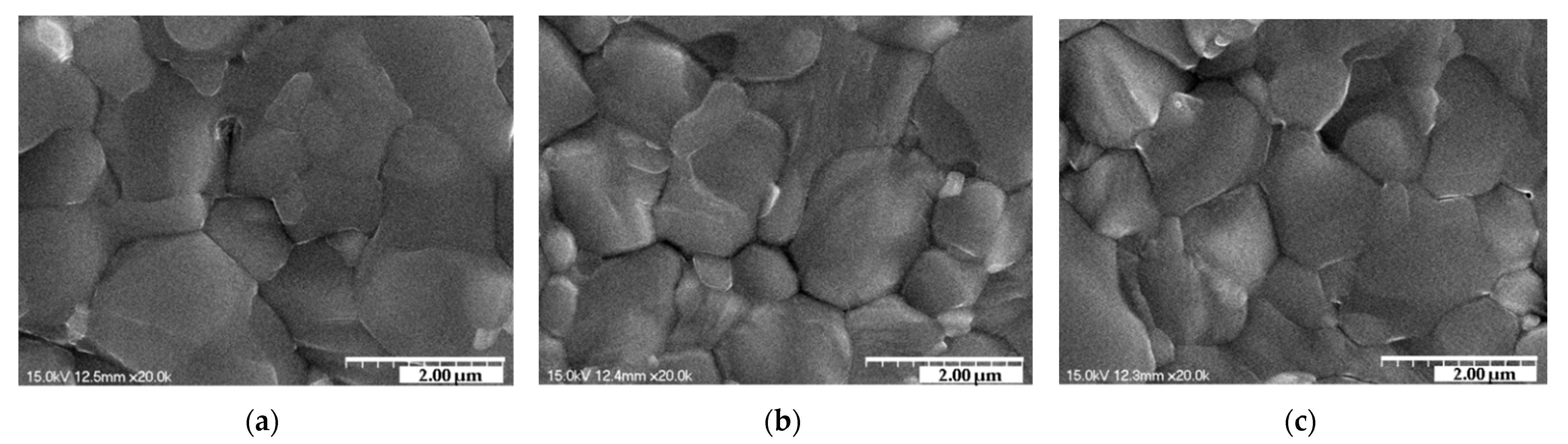
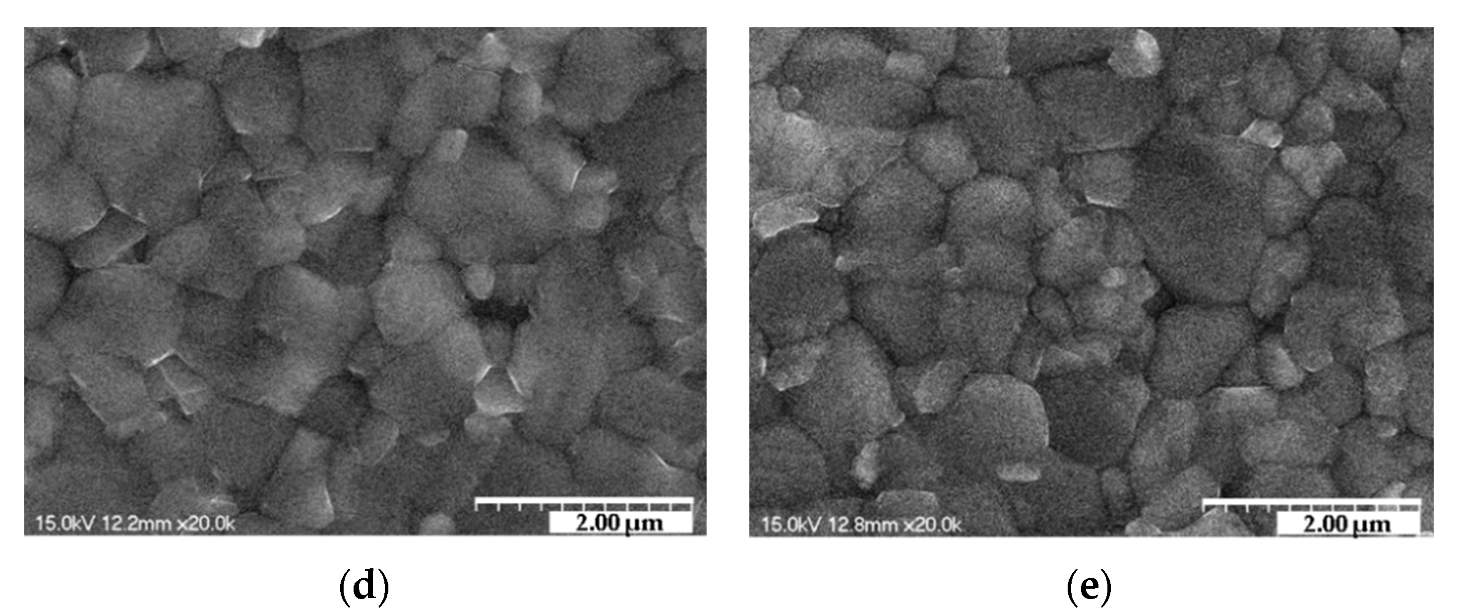
Figure 3 displays SEM images of the (FAPbI3)1−x(MAPbBr3)x perovskite films; it confirms that a change in the composition ratio x affects the film surface. The average diameter lengths of the grain of (FAPbI3)1−x(MAPbBr3)x films (x = 0, 0.03, 0.05, 0.07, 0.1) were 1.629, 1.496, 1.465, 0.922, and 0.815 um. In Figure 3a–c, the grain size decreased as x increased. This is because MA+ (2.70 Å) has a smaller particle size than FA+ (2.79 Å), and Br− (1.96 Å) has a smaller particle size than I− (2.2 Å) [32,35]; as such, when x increases, more MA+ and Br− replace FA+ and I− [36]. However, compared to when x = 0.07, the difference in the small grain diameter increase was not significant.
Figure 3d,e show the sharply reduced grain size. Additionally, a residue was observed when x = 0.1 because a portion of MAPbBr3 was decomposed, at because of the high annealing temperature of 150 °C, forming PbI2 and PbBr2. This suggests that the perovskite was not well-formed at this composition ratio. A small grain size with many crystals observed on the surface leads to deterioration of performance. As residues are produced and replaced with smaller ions, resulting in a smaller grain size, the mobility of carrier transport decreases, which, in turn, increases carrier scattering, leading to poor performance [37].
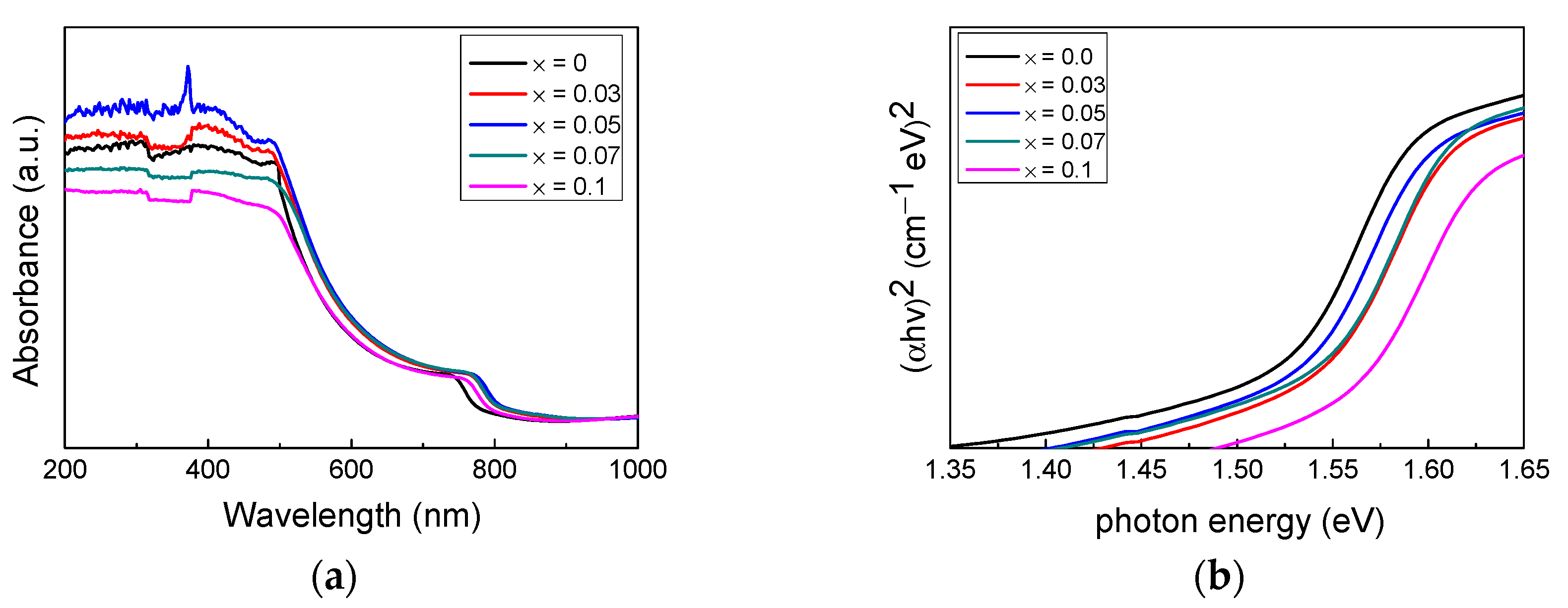
Figure 4a presents the optical absorption spectra of the (FAPbI3)1−x(MAPbBr3)x films (x = 0, 0.03, 0.05, 0.07, and 0.1). All (FAPbI3)1−x(MAPbBr3)x samples displayed a strong absorbance at 200–500 nm. This demonstrates that the (FAPbI3)1−x(MAPbBr3)x-based photodetector sufficiently detected light in the UVC region. The absorbance increased as the value of x increased but decreased when the value of x exceeded 0.07. This suggests that certain (FAPbI3)1−x(MAPbBr3)x compositions (x = 0.03 and 0.05) have better light absorption characteristics than pure FAPbI3.
Figure 4b is an estimated Tauc plot based on the light absorption of the (FAPbI3)1−x(MAPbBr3)x (x = 0, 0.03, 0.05, 0.07, and 0.1) films. The sharp band energies indicate the presence of a direct bandgap. Semiconductors with wide bandgaps can absorb and emit high-energy photons, enabling the fabrication of high-performance photonic devices, including UV detectors [38]. Based on the light absorption characteristics, the bandgap of pure FAPbI3 and (FAPbI3)1−x(MAPbBr3)x (x = 0.03, 0.05, and 0.07) was estimated to be 1.45 eV and 1.52 eV, respectively. The increase in the band gap was due to the structural distortion caused by the stress on the Pb–I bond resulting from the incorporation of Br [36]. Changes in the kinetic energy of the electron-hole pairs due to Coulomb interactions also result in bandgap differences [39]. The largest bandgap of 1.55 eV was observed when x = 0.1. However, PbI2 residues are likely to be present when x = 0.1 [36].
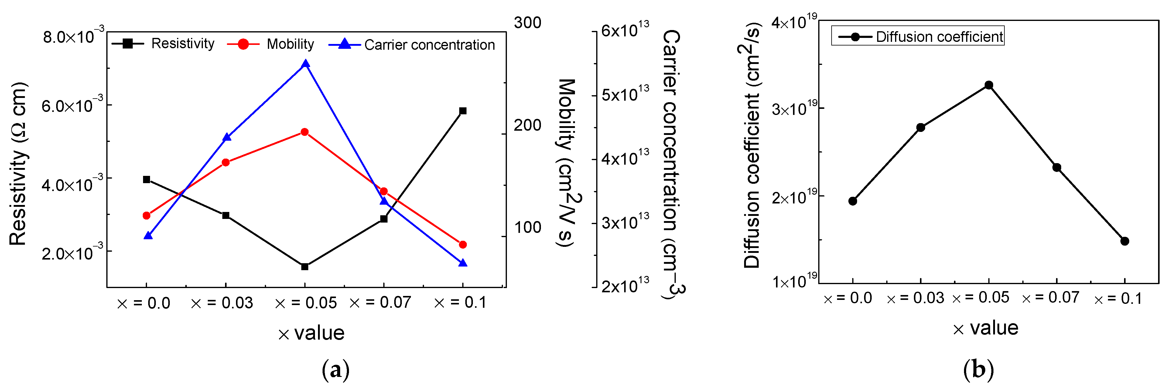
Figure 5a shows the electrical properties (resistivity, mobility, and carrier concentration) of the (FAPbI3)1−x(MAPbBr3)x thin films (x = 0, 0.03, 0.05, 0.07, and 0.1). The resistivity of (FAPbI3)1−x(MAPbBr3)x decreased as the x value increased, except for x = 0.1. In particular, (FAPbI3)0.95(MAPbBr3)0.05 displayed the lowest resistivity, i.e., 0.00157 Ω cm.
Carrier concentration and mobility are significant parameters for semiconductor materials and electronic power devices [40]. All (FAPbI3)1−x(MAPbBr3)x films had carrier concentration values higher than 1013 cm−3. The current depends on the mobility; the higher the mobility, the higher the current [38,41,42]. The mobilities of the (FAPbI3)1−x(MAPbBr3)x films were 120.3, 172.2, 202.2, 144, and 91.9 cm2/V.s for x values of 0, 0.03, 0.05, 0.07, and 0.1, respectively.
Figure 5b shows the diffusion coefficient (D) of the (FAPbI3)1−x(MAPbBr3)x films (x = 0, 0.03, 0.05, 0.07, and 0.1). D is related to the mobility, as shown in Figure 5a. Diffusion involves the movement of charge carriers driven by a concentration gradient [14,43]. In the presence of a magnetic field, D is defined using the Einstein relation D = μKT/q, where μ is mobility, K is the Boltzmann constant, T is the temperature of the sample, and q is the amount of charge [43]. The D of the (FAPbI3)1−x(MAPbBr3)x films increased as the x value increased, except for x = 0.1. The charge carrier LD was calculated as LD = √Dτ, where τ is the lifetime [44]. The mobility and LD are proportional, and high mobility leads to an increase in the D and LD values. When I− is replaced by Br−, the lattice parameters shrink, leading to an increase in the photogenerated carrier lifetime and the charge carrier mobility [33,45]. Combining the results in Figure 5, it shows that the (FAPbI3)1−x(MAPbBr3)x film had the best electrical properties such as carrier concentration and mobility when x = 0.05.
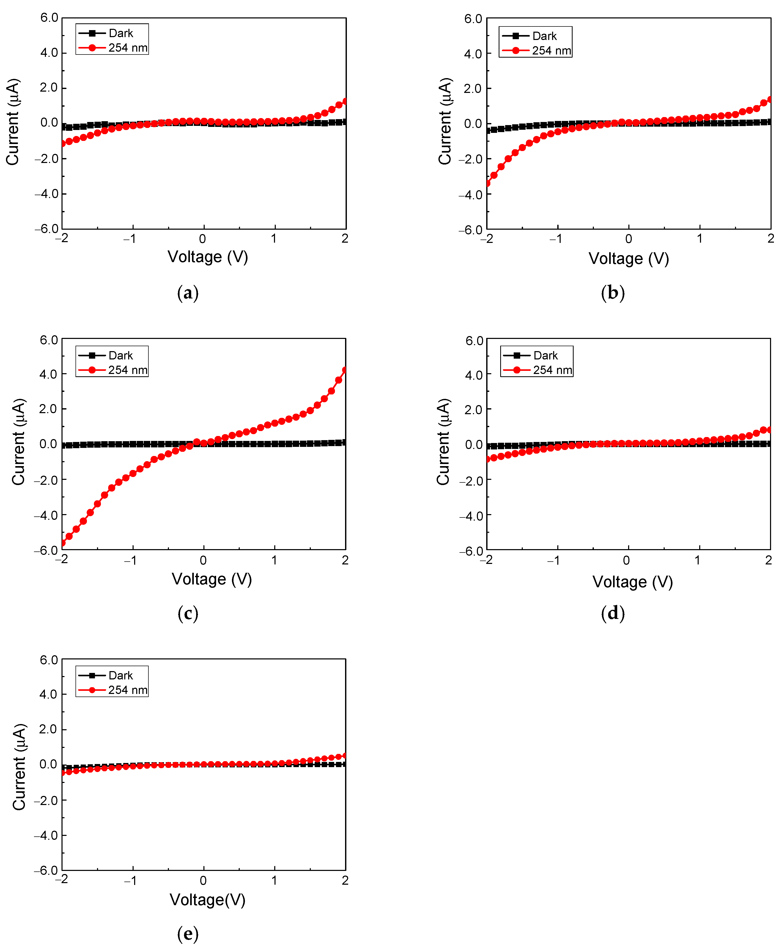
In addition, to analyze the performance of the (FAPbI3)1−x(MAPbBr3)x (x = 0, 0.03, 0.05, 0.07, and 0.1) photodetectors, the current-voltage (I–V) characteristics were measured from −2 V to 2 V at a scan rate of 0.1 V. Measurements were performed in a dark environment and under a 254 nm light source with an output of 0.6 mW/cm2. In the perovskite photodetector, a Schottky barrier formed owing to the contact with the ITO electrode, and the current flowed through it.
Figure 6a–e show that the(FAPbI3)1−x(MAPbBr3)x photodetectors were barely able to detect 254 nm light at 0.6 mW/cm2 in a dark environment. However, the (FAPbI3)0.95(MAPbBr3)0.05 photodetector generated significant photocurrents of −5.61 µA at −2 V and 4.2 µA at 2 V under 254 nm irradiation with an output of 0.6 mW/cm2, as shown in Figure 6c.
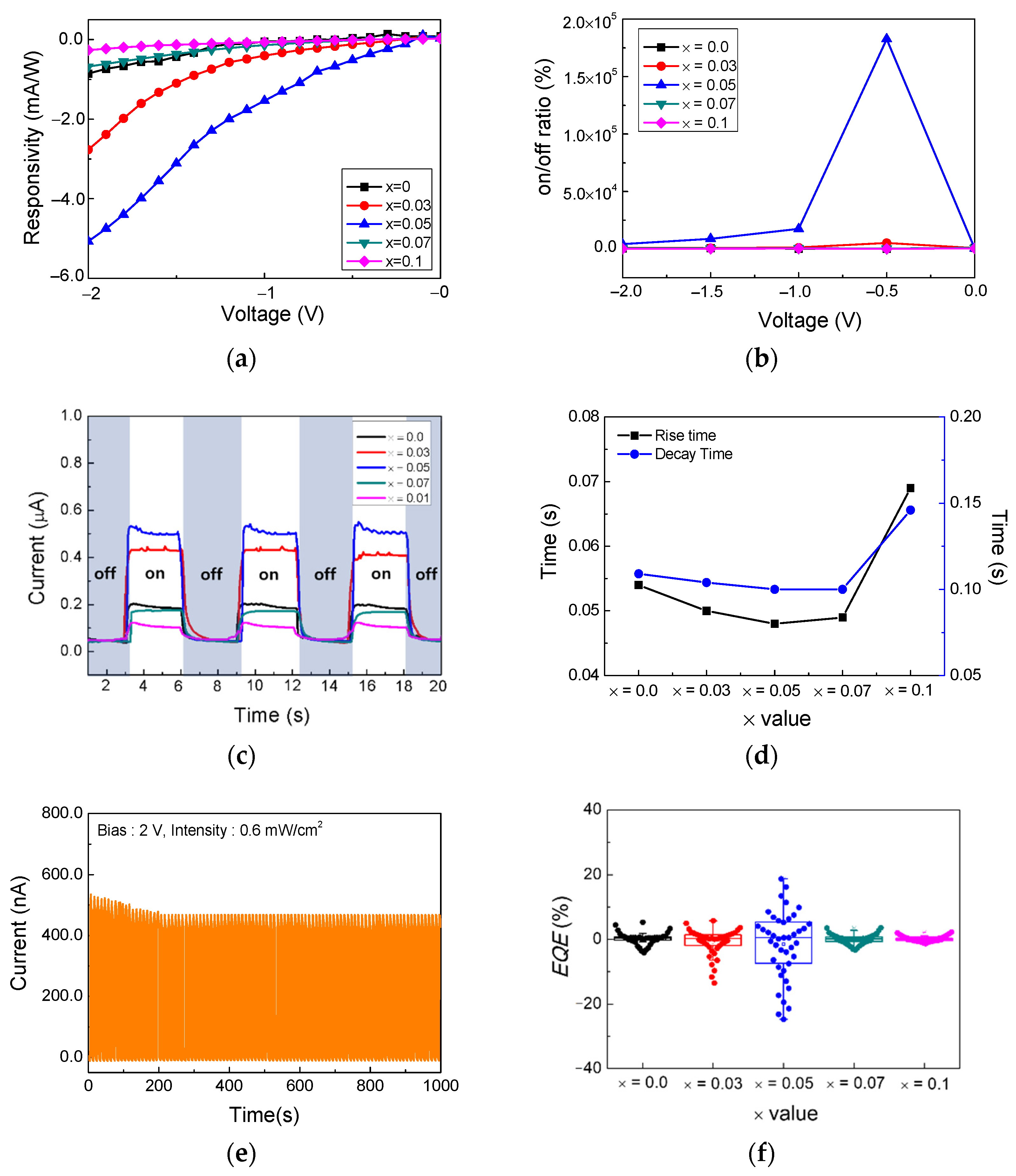
To evaluate the performance of the photodetector, the significant parameters of the detector under a light of 254 nm with an output of 0.6 mW/cm2 were investigated. Figure 7a shows the responsivity (R) of the films. R is the main parameter that indicates the performance of the photodetector and the response of the device to the irradiated light. R is defined as R = (I254 − Idark)/P × S mA/W [14], where I254 is the current when irradiated with 254 nm light, Idark is the dark environment current, P is the power of the incident light, and S is the irradiated area of the device [46]. R gradually decreased as the bias decreased owing to the change in the photon-charge conversion efficiency of the photodetector [10]. Under 254 nm illumination, with an output of 0.6 mW/cm2, the R values of (FAPbI3)1−x(MAPbI3)x were 0.85, 2.77, 5.07, 0.68, and 0.26 mA/W at −2 V when x was 0, 0.03, 0.05, 0.07, and 0.1, respectively.
Figure 7b shows the on/off ratios of the (FAPbI3)1−x(MAPbBr3)x photodetectors in the reverse bias region from −2 V to 0 V. A high on/off ratio is related to good performance in a photodetector [11]. The on/off ratios at −2 V were 539, 835, 4211, 663, and 258% for x = 0, 0.03, 0.05, 0.07, and 0.1, respectively. Additionally, when the voltage was −0.5 V, the largest on/off ratio was observed for x = 0.05.
Figure 7c,d show the time dependent response of the (FAPbI3)1−x(MAPbBr3)x photodetectors. An on/off switching test was performed to observe transient photoresponses under 254 nm radiation with an 0.6 mA/cm2 intensity at a 2 V bias. Response times, such as rise and decay times, could be inferred from the relative speed of response of the detector to changes in the optical signal. Figure 7c shows that during on/off switching, the (FAPbI3)1−x(MAPbBr3)x (x = 0.03 and 0.05) photodetectors exhibited a higher photo-response than pure FAPbI3. In addition, Figure 7d shows that when the x value was 0.05, the (FAPbI3)1−x(MAPbBr3)x photodetectors had the smallest rise and decay times, i.e., 0.048 and 0.1 s, respectively. Therefore, the (FAPbI3)0.95(MAPbBr3)0.05 photodetector had the fastest photo-response among all the photodetectors, and is highly sensitive.
Figure 7e shows the on/off repeatability of the (FAPbI3)0.95(MAPbBr3)0.05 photodetector. The on/off switch was irradiated for 1000 s using a 254 nm light source with an output of 0.6 mW/cm2. In the first on/off iteration, the photocurrent was 523 nA. The light was irradiated for 5 s, and the photodetector was cycled on/off 100 times. After 100 cycles, the photocurrent decreased slightly to 468 nA, but remained constant from the 16th cycle to the 100th cycle. Although a slight decrease in photocurrent was observed, the maintenance of the photocurrent over a relatively long time proves its reproducibility.
EQE, which is the number of electrons produced per incident photon, is another important parameter that indicates the detector performance. EQE is defined as Rhc/eλ, where R is the responsivity, h is the Planck constant, c is the speed of light, e is the electron charge, and λ is the wavelength of the light [9]. Figure 7f shows the EQE from −2 V to 2 V bias as a box plot under 254 nm light irradiation with 0.6 mA/cm2 intensity. Figure 7c shows that the EQE increases up to x = 0.05 and decreases at x = 0.07. These results exhibit the same pattern as the other measurements (XRD, UV-vis, and responsivity measurements) and demonstrate that among the (FAPbI3)1−x(MAPbBr3)x (x = 0, 0.03, 0.05, 0.07, and 0.1) photodetectors, the (FAPbI3)0.95(MAPbBr3)0.05 composition exhibited the best optical properties.
Detectivity D* is an important photodetector parameter, defined as D* = R/(2qJdark)1/2, where R is the responsivity, q is the electron charge, and Jdark is the current density of the dark current [14,38]. In Table 1, parameters, such as R, D, and EQE, of UVC photodetectors fabricated using various materials are listed. The R and EQE values of the (FAPbI3)0.95(MAPbBr3)0.05 photodetector fabricated in this study were superior to those of photodetectors reported in other studies. This suggests that the perovskite-based UVC photodetectors fabricated in this study are promising candidates in the field of UVC sensing, as the perovskites can be fabricated using a simple process at lower temperatures than those of previously reported photodetectors. In addition, the R and EQE values were superior to those of perovskite-based photodetectors reported in other studies, while the D* values were similar. These results indicate that (FAPbI3)0.95(MAPbBr3)0.05 is a promising material for developing perovskite-based photodetectors.
4. Conclusions
Mixed cation–halide perovskite (FAPbI3)1−x(MAPbBr3)x (x = 0, 0.03, 0.05, 0.07, and 0.1)-based photodetectors were investigated. (FAPbI3)1−x(MAPbBr3)x films exhibited the most improved stability and light absorption when the MAPbBr3 ratio was 5 mol%. The (FAPbI3)0.95(MAPbBr3)0.05 UVC photodetector exhibited an EQE of 24.8%, a mobility of 202.2 cm2/Vs, a response of 5.07 mA/W, and a detection rate of 5.49 × 10¹¹ Jones. These are excellent parameter values compared with previously reported values for perovskite-based photodetectors fabricated using the solution process. By applying the process described in this study, it is possible to fabricate a photodetector with improved optical properties through a low-energy process. This suggests that mixed cation–halide perovskite-based photodetectors have significant potential for use in UVC photodetectors.
Author Contributions
Investigation, G.I.C.; Validation G.I.C. and H.W.C.; Writing—original draft preparation, G.I.C.; Writing—review and editing, G.I.C. and H.W.C.; Supervision, H.W.C. All authors have read and agreed to the published version of the manuscript.
Funding
This research was supported by the Basic Science Research Capacity Enhancement Project through the Korea Basic Science Institute (National Research Facilities and Equipment Center) grant funded by the Ministry of Education (2019R1A6C1010016). This work was supported by the Gachon University research fund of 2020 (GCU-202008450009).
Institutional Review Board Statement
Not applicable.
Informed Consent Statement
Not applicable.
Data Availability Statement
The data is available on reasonable request from the corresponding author.
Conflicts of Interest
The authors declare no conflict of interest.
References
- Leung, S.F.; Ho, K.T.; Kung, P.K.; Hsiao, V.K.; Alshareef, H.N.; Wang, Z.L.; He, J.H. A self-powered and flexible organometallic halide perovskite photodetector with very high detectivity. Adv. Mater. 2018, 30, 1704611. [Google Scholar]
- Li, C.; Ma, Y.; Xiao, Y.; Shen, L.; Ding, L. Advances in perovskite photodetectors. InfoMat 2020, 2, 1247–1256. [Google Scholar]
- Fang, F.; Li, H.; Fang, S.; Zhou, B.; Huang, F.; Ma, C.; Wan, Y.; Jiang, S.; Wang, Y.; Tian, B.; et al. 2D Cs2AgBiBr6 with Boosted Light–Matter Interaction for High-Performance Photodetectors. Adv. Opt. Mater. 2021, 9, 2001930. [Google Scholar]
- Yang, W.; Chen, J.; Zhang, Y.; Zhang, Y.; He, J.H.; Fang, X. Silicon-compatible photodetectors: Trends to monolithically integrate photosensors with chip technology. Adv. Funct. Mater. 2019, 29, 1808182. [Google Scholar]
- Yao, J.; Yang, G. 2D material broadband photodetectors. Nanoscale 2020, 12, 454–476. [Google Scholar]
- Tsai, S.H.; Basu, S.; Huang, C.Y.; Hsu, L.C.; Lin, Y.G.; Horng, R.H. Deep-ultraviolet photodetectors based on epitaxial ZnGa2O4 thin films. Sci. Rep. 2018, 8, 14056. [Google Scholar] [CrossRef]
- Guo, D.; Liu, H.; Li, P.; Wu, Z.; Wang, S.; Cui, C.; Li, C.; Tang, W. Zero-power-consumption solar-blind photodetector based on β-Ga2O3/NSTO heterojunction. ACS Appl. Mater. Interfaces 2017, 9, 1619–1628. [Google Scholar]
- Park, T.; Hur, J. Self-Powered Low-Cost UVC Sensor Based on Organic-Inorganic Heterojunction for Partial Discharge Detection. Small 2021, 17, 2100695. [Google Scholar]
- Preto, S.; Gomes, C.C. Ultraviolet radiation in sunlight and artificial lighting systems: Are they alike? In International Conference on Applied Human Factors and Ergonomics; Springer: Cham, Germany, 2017; pp. 287–298. [Google Scholar]
- Nguyen, T.M.H.; Kim, S.; Bark, C.W. Solution-processed and self-powered photodetector in vertical architecture using mixed-halide perovskite for highly sensitive UVC detection. J. Mater. Chem. A 2021, 9, 1269–1276. [Google Scholar] [CrossRef]
- Nguyen, T.M.H.; Lee, S.K.; Kim, S.; Bark, C.W. Practical Demonstration of Deep-Ultraviolet Detection with Wearable and Self-Powered Halide Perovskite-Based Photodetector. ACS Appl. Mater. Interfaces 2021, 13, 57609–57618. [Google Scholar]
- Ertle, D.; Friedl, R.; Vogel, F.; Fantz, U. Experimental Investigation and Modelling of the Spectral Intensity of the N2-Emission in Argon Low-Pressure Arc Discharges. In Proceedings of the 30th International Conference on Phenomena in Ionized Gases (ICPIG 2011), Belfast, UK, 29 August–2 September 2011; p. D15. [Google Scholar]
- Dixon, A.J.; Dixon, B.F. Ultraviolet radiation from welding and possible risk of skin and ocular malignancy. Med. J. Aust. 2004, 181, 155–157. [Google Scholar] [CrossRef]
- Shin, S.G.; Bark, C.W.; Choi, H.W. Study on Performance Improvements in Perovskite-Based Ultraviolet Sensors Prepared Using Toluene Antisolvent and CH3NH3Cl. Nanomaterials 2021, 11, 1000. [Google Scholar] [CrossRef]
- Ferreira, S.H.; Cunha, I.; Pinto, J.V.; Neto, J.P.; Pereira, L.; Fortunato, E.; Martins, R. UV-Responsive Screen-Printed Porous ZnO Nanostructures on Office Paper for Sustainable and Foldable Electronics. Chemosensors 2021, 9, 192. [Google Scholar] [CrossRef]
- Claro, P.I.; Marques, A.C.; Cunha, I.; Martins, R.F.P.; Pereira, L.M.; Marconcini, J.M.; Mattoso, L.H.C.; Fortunato, E. Tuning the electrical properties of cellulose nanocrystals through laser-induced graphitization for UV photodetectors. ACS Appl. Nano Mater. 2021, 4, 8262–8272. [Google Scholar] [CrossRef]
- Figueira, J.; Gaspar, C.; Carvalho, J.T.; Loureiro, J.; Fortunato, E.; Martins, R.; Pereira, L. Sustainable fully printed UV sensors on cork using zinc oxide/ethylcellulose inks. Micromachines 2019, 10, 601. [Google Scholar] [CrossRef] [Green Version]
- Ju, Z.G.; Shan, C.X.; Jiang, D.Y.; Zhang, J.Y.; Yao, B.; Zhao, D.X.; Shen, D.Z.; Fan, X.W. MgxZn1−xO-based photodetectors covering the whole solar-blind spectrum range. Appl. Phys. Lett. 2008, 93, 173505. [Google Scholar] [CrossRef]
- Gu, S.; Lin, R.; Han, Q.; Gao, Y.; Tan, H.; Zhu, J. Tin and mixed lead–tin halide perovskite solar cells: Progress and their application in tandem solar cells. Adv. Mater. 2020, 32, 1907392. [Google Scholar] [CrossRef]
- Bibi, A.; Lee, I.; Nah, Y.; Allam, O.; Kim, H.; Quan, L.N.; Tang, J.; Walsh, A.; Jang, S.S.; Sargent, E.H.; et al. Lead-free halide double perovskites: Toward stable and sustainable optoelectronic devices. Mater. Today 2021, 49, 123–144. [Google Scholar] [CrossRef]
- Li, Y.; Shi, Z.F.; Li, X.J.; Shan, C.X. Photodetectors based on inorganic halide perovskites: Materials and devices. Chin. Phys. B 2019, 28, 017803. [Google Scholar] [CrossRef]
- Imran, M.; Khan, N.A. Perovskite phase formation in formamidinium–methylammonium lead iodide bromide (FAPbI3)1−x(MAPbBr3)x materials and their morphological, optical and photovoltaic properties. Appl. Phys. A 2019, 125, 575. [Google Scholar] [CrossRef]
- Tong, G.; Li, H.; Zhu, Z.; Zhang, Y.; Yu, L.; Xu, J.; Jiang, Y. Enhancing hybrid perovskite detectability in the deep ultraviolet region with down-conversion dual-phase (CsPbBr3–Cs4PbBr6) films. J. Phys. Chem. Lett. 2018, 9, 1592–1599. [Google Scholar] [CrossRef]
- Guo, X.; Ngai, K.; Qin, M.; Lu, X.; Xu, J.; Long, M. The compatibility of methylammonium and formamidinium in mixed cation perovskite: The optoelectronic and stability properties. Nanotechnology 2020, 32, 075406. [Google Scholar] [CrossRef]
- Zhou, D.; Zhou, T.; Tian, Y.; Zhu, X.; Tu, Y. Perovskite-based solar cells: Materials, methods, and future perspectives. J. Nanomater. 2018, 2018, 8148072. [Google Scholar] [CrossRef]
- Ava, T.T.; Al Mamun, A.; Marsillac, S.; Namkoong, G. A review: Thermal stability of methylammonium lead halide based perovskite solar cells. Appl. Sci. 2019, 9, 188. [Google Scholar] [CrossRef] [Green Version]
- Reyna, Y.; Salado, M.; Kazim, S.; Perez-Tomas, A.; Ahmad, S.; Lira-Cantu, M. Performance and stability of mixed FAPbI3(0.85)MAPbBr3(0.15) halide perovskite solar cells under outdoor conditions and the effect of low light irradiation. Nano Energy 2016, 30, 570–579. [Google Scholar] [CrossRef] [Green Version]
- Li, W.G.; Rao, H.S.; Chen, B.X.; Wang, X.D.; Kuang, D.B. A formamidinium–methylammonium lead iodide perovskite single crystal exhibiting exceptional optoelectronic properties and long-term stability. J. Mater. Chem. A 2017, 5, 19431–19438. [Google Scholar] [CrossRef]
- Lee, J.W.; Seol, D.J.; Cho, A.N.; Park, N.G. High-efficiency perovskite solar cells based on the black polymorph of HC (NH2)2PbI3. Adv. Mater. 2014, 26, 4991–4998. [Google Scholar] [CrossRef]
- Wang, M.; Cao, F.; Deng, K.; Li, L. Adduct phases induced controlled crystallization for mixed-cation perovskite solar cells with efficiency over 21%. Nano Energy 2019, 63, 103867. [Google Scholar] [CrossRef]
- Chen, L.; Cao, H.; Wang, S.; Luo, Y.; Tao, T.; Sun, J.; Zhang, M. Efficient air-stable perovskite solar cells with a (FAI)0.46(MAI)0.40 (MABr)0.14(PbI2)0.86(PbBr2)0.14 active layer fabricated via a vacuum flash-assisted method under RH > 50%. RSC Adv. 2019, 9, 10148–10154. [Google Scholar] [CrossRef] [Green Version]
- Tang, S.; Xiao, X.; Hu, J.; Gao, B.; Chen, H.; Zuo, Z.; Qi, Q.; Peng, Z.; Wen, J.; Zou, D. Mechanochemical synthesis of pure phase mixed-cation/anion (FAPbI3)x(MAPbBr3)1−x hybrid perovskite materials: Compositional engineering and photovoltaic performance. RSC Adv. 2021, 11, 5874–5884. [Google Scholar] [CrossRef]
- Tumusange, M.S.; Subedi, B.; Chen, C.; Junda, M.M.; Song, Z.; Yan, Y.; Podraza, N.J. Impact of Humidity and Temperature on the Stability of the Optical Properties and Structure of MAPbI3, MA0.7FA0.3PbI3 and (FAPbI3)0.95(MAPbBr3)0.05 Perovskite Thin Films. Materials 2021, 14, 4054. [Google Scholar] [CrossRef] [PubMed]
- Xu, F.; Zhang, T.; Li, G.; Zhao, Y. Mixed cation hybrid lead halide perovskites with enhanced performance and stability. J. Mater. Chem. A 2017, 5, 11450–11461. [Google Scholar] [CrossRef]
- Li, X.; Yang, J.; Jiang, Q.; Chu, W.; Zhang, D.; Zhou, Z.; Ren, Y.; Xin, J. Enhanced photovoltaic performance and stability in mixed-cation perovskite solar cells via compositional modulation. Electrochim. Acta 2017, 247, 460–467. [Google Scholar] [CrossRef]
- Atourki, L.; Vega, E.; Marí, B.; Mollar, M.; Ahsaine, H.A.; Bouabid, K.; Ihlal, A. Role of the chemical substitution on the structural and luminescence properties of the mixed halide perovskite thin MAPbI3−xBrx (0 ≤ x ≤ 1) films. Appl. Surf. Sci. 2016, 371, 112–117. [Google Scholar] [CrossRef]
- Chen, L.C.; Tseng, Z.L.; Huang, J.K.; Chen, C.C.; Chang, S.H. Fullerene-based Electron transport layers for semi-transparent MAPbBr3 perovskite films in planar perovskite solar cells. Coatings 2016, 6, 53. [Google Scholar] [CrossRef] [Green Version]
- Zou, Y.; Zhang, Y.; Hu, Y.; Gu, H. Ultraviolet detectors based on wide bandgap semiconductor nanowire: A review. Sensors 2018, 18, 2072. [Google Scholar] [CrossRef] [Green Version]
- Mosconi, E.; Amat, A.; Nazeeruddin, M.K.; Gratzel, M.; De Angelis, F. First-principles modeling of mixed halide organometal perovskites for photovoltaic applications. J. Phys. Chem. C 2013, 117, 13902–13913. [Google Scholar] [CrossRef]
- Koizumi, S.; Umezawa, H.; Pernot, J.; Suzuki, M. 2-Doping and Semiconductor Characterizations. In Power Electronics Device Applications of Diamond Semiconductors; Woodhead Publishing: Sawston, UK, 2018; pp. 99–189. [Google Scholar]
- Bercegol, A.; Ory, D.; Suchet, D.; Cacovich, S.; Fournier, O.; Rousset, J.; Lombez, L. Quantitative optical assessment of photonic and electronic properties in halide perovskite. Nat. Commun. 2019, 10, 1586. [Google Scholar] [CrossRef] [Green Version]
- Myronov, M. Molecular Beam Epitaxy of High Mobility Silicon, Silicon Germanium and Germanium Quantum Well Heterostructures. In Molecular Beam Epitaxy; Elsevier: Amsterdam, The Netherlands, 2018; pp. 37–54. [Google Scholar]
- Hodes, G.; Kamat, P.V. Understanding the implication of carrier diffusion length in photovoltaic cells. J. Phys. Chem. Lett. 2015, 6, 4090–4092. [Google Scholar] [CrossRef] [Green Version]
- Li, Y.; Yan, W.; Li, Y.; Wang, S.; Wang, W.; Bian, Z.; Xiao, L.; Gong, Q. Direct observation of long electron-hole diffusion distance in CH3NH3PbI3 perovskite thin film. Sci. Rep. 2015, 5, 14485. [Google Scholar] [CrossRef]
- Lin, C.; Li, S.; Zhang, W.; Shao, C.; Yang, Z. Effect of bromine substitution on the ion migration and optical absorption in MAPbI3 perovskite solar cells: The first-principles study. ACS Appl. Energy Mater. 2018, 1, 1374–1380. [Google Scholar] [CrossRef]
- Chen, J.H.; Jing, Q.; Xu, F.; Lu, Y.Q. High-sensitivity optical-fiber-compatible photodetector with an integrated CsPbBr3–graphene hybrid structure. Optica 2017, 4, 835–838. [Google Scholar] [CrossRef]
- Zhang, T.; Wang, F.; Zhang, P.; Wang, Y.; Chen, H.; Li, J.; Wu, J.; Chen, L.; Chen, Z.D.; Li, S. Low-temperature processed inorganic perovskites for flexible detectors with a broadband photoresponse. Nanoscale 2019, 11, 2871–2877. [Google Scholar] [CrossRef] [PubMed]
- Tran, M.H.; Park, T.; Hur, J. Wide-bandgap CaSnO3 perovskite as an efficient and selective deep-UV absorber for self-powered and high-performance pin photodetector. ACS Appl. Mater. Interfaces 2021, 13, 13372–13382. [Google Scholar] [CrossRef]
- Zhang, Q.; Jie, J.; Diao, S.; Shao, Z.; Zhang, Q.; Wang, L.; Deng, W.; Hu, W.; Xia, H.; Yuan, X.; et al. Solution-processed graphene quantum dot deep-UV photodetectors. ACS Nano 2015, 9, 1561–1570. [Google Scholar] [CrossRef]
- Xia, Y.; Zhai, G.; Zheng, Z.; Lian, L.; Liu, H.; Zhang, D.; Gao, J.; Zhai, T.; Zhang, J. Solution-processed solar-blind deep ultraviolet photodetectors based on strongly quantum confined ZnS quantum dots. J. Mater. Chem. C 2018, 6, 11266–11271. [Google Scholar] [CrossRef]
Figure 1.
(a) Schematic and (b) fabrication process of the (FAPbI3)1−x(MAPbBr3)x photodetector.

Figure 2.
Crystal structure of (FAPbI3)1−x(MAPbBr3)x films. (a) XRD patterns for different composition ratios (x = 0, 0.03, 0.05, 0.07, and 0.01) and (b) XRD patterns in the 13.0–15.0° range.
Figure 2.
Crystal structure of (FAPbI3)1−x(MAPbBr3)x films. (a) XRD patterns for different composition ratios (x = 0, 0.03, 0.05, 0.07, and 0.01) and (b) XRD patterns in the 13.0–15.0° range.

Figure 3.
SEM images of (FAPbI3)1−x(MAPbBr3)x films for different composition ratios: (a) x = 0, (b) x = 0.03, (c) x = 0.05, (d) x = 0.07, and (e) x = 0.1.
Figure 3.
SEM images of (FAPbI3)1−x(MAPbBr3)x films for different composition ratios: (a) x = 0, (b) x = 0.03, (c) x = 0.05, (d) x = 0.07, and (e) x = 0.1.


Figure 4.
Light absorption and bandgap of (FAPbI3)1−x(MAPbBr3)x films (x = 0, 0.03, 0.05, 0.07, and 0.01). (a) UV-vis absorbance spectra and (b) Tauc plot.
Figure 4.
Light absorption and bandgap of (FAPbI3)1−x(MAPbBr3)x films (x = 0, 0.03, 0.05, 0.07, and 0.01). (a) UV-vis absorbance spectra and (b) Tauc plot.

Figure 5.
(a) Comparison of electrical characteristics including resistivity, carrier concentration and mobility, (b) diffusion coefficients of (FAPbI3)1−x(MAPbBr3)x films (x = 0, 0.03, 0.05, 0.07, and 0.01).
Figure 5.
(a) Comparison of electrical characteristics including resistivity, carrier concentration and mobility, (b) diffusion coefficients of (FAPbI3)1−x(MAPbBr3)x films (x = 0, 0.03, 0.05, 0.07, and 0.01).

Figure 6.
Current–voltage characteristics of (FAPbI3)1−x(MAPbBr3)x photodetectors for different composition ratios: (a) x = 0, (b) x = 0.03, (c) x = 0.05, (d) x = 0.07, and (e) x = 0.1.
Figure 6.
Current–voltage characteristics of (FAPbI3)1−x(MAPbBr3)x photodetectors for different composition ratios: (a) x = 0, (b) x = 0.03, (c) x = 0.05, (d) x = 0.07, and (e) x = 0.1.

Figure 7.
(FAPbI3)1−x(MAPbBr3)x photodetector response. (a) Responsivity curves, (b) on/off ratio, (c) transient photo-responses, (d) rise and decay times, (e) photostability of the prepared device switching under the illumination of 254 nm light with an intensity of 0.6 mW/cm2, and (f) external quantum efficiency.


Table 1.
Comparison of UVC various photodetector parameters.
| Materials | Light (nm) | Bias (V) | R (mA/W) | D* (Jones) | EQE (%) | Ref. |
|---|---|---|---|---|---|---|
| (FAPbI3)0.95(MAPbI3)0.05 | 254 | −2 | 5.07 | 5.49 × 10¹¹ | 24.8 | [In this study] |
| (FAPbI3)1−x(MAPbBr3)x | 254 | 0 | 4.92 | 7.57 × 10¹⁰ | - | [11] |
| MAPbBr3 | 254 | 2 | 4.57 | 1.02 × 10¹³ | 22.2 | [14] |
| CsPbBr3/ | 254 | 2 | 0.24 | 1.1 × 10⁹ | 0.05 | [47] |
| CaSnO3 | 255 | 0 | 2.25 | 1.56 × 10¹⁰ | 1.06 | [48] |
| Ag/GQD/Au | 254 | 5 | 2.1 | 9.59 × 10¹¹ | 10.3 | [49] |
| Mn0.52Zn0.48O | 250 | 10 | 0.1 | - | - | [18] |
| Nb:SrTiO3/Ga2O3 | 254 | 0 | 2.6 | - | 1.3 | [7] |
| Au/ZnS QDs/Au | 254 | 40 | 0.077 | - | - | [50] |
Publisher’s Note: MDPI stays neutral with regard to jurisdictional claims in published maps and institutional affiliations. |
© 2022 by the authors. Licensee MDPI, Basel, Switzerland. This article is an open access article distributed under the terms and conditions of the Creative Commons Attribution (CC BY) license (https://creativecommons.org/licenses/by/4.0/).
Share and Cite
MDPI and ACS Style
Choi, G.I.; Choi, H.W. A Study to Improve the Performance of Mixed Cation–Halide Perovskite-Based UVC Photodetectors. Nanomaterials 2022, 12, 1132. https://0-doi-org.brum.beds.ac.uk/10.3390/nano12071132
AMA Style
Choi GI, Choi HW. A Study to Improve the Performance of Mixed Cation–Halide Perovskite-Based UVC Photodetectors. Nanomaterials. 2022; 12(7):1132. https://0-doi-org.brum.beds.ac.uk/10.3390/nano12071132
Chicago/Turabian StyleChoi, Ga In, and Hyung Wook Choi. 2022. "A Study to Improve the Performance of Mixed Cation–Halide Perovskite-Based UVC Photodetectors" Nanomaterials 12, no. 7: 1132. https://0-doi-org.brum.beds.ac.uk/10.3390/nano12071132
Note that from the first issue of 2016, this journal uses article numbers instead of page numbers. See further details here.