

Overview of Engineering Carbon Nanomaterials Such As Carbon Nanotubes (CNTs), Carbon Nanofibers (CNFs), Graphene and Nanodiamonds and Other Carbon Allotropes inside Porous Anodic Alumina (PAA) Templates

Abstract
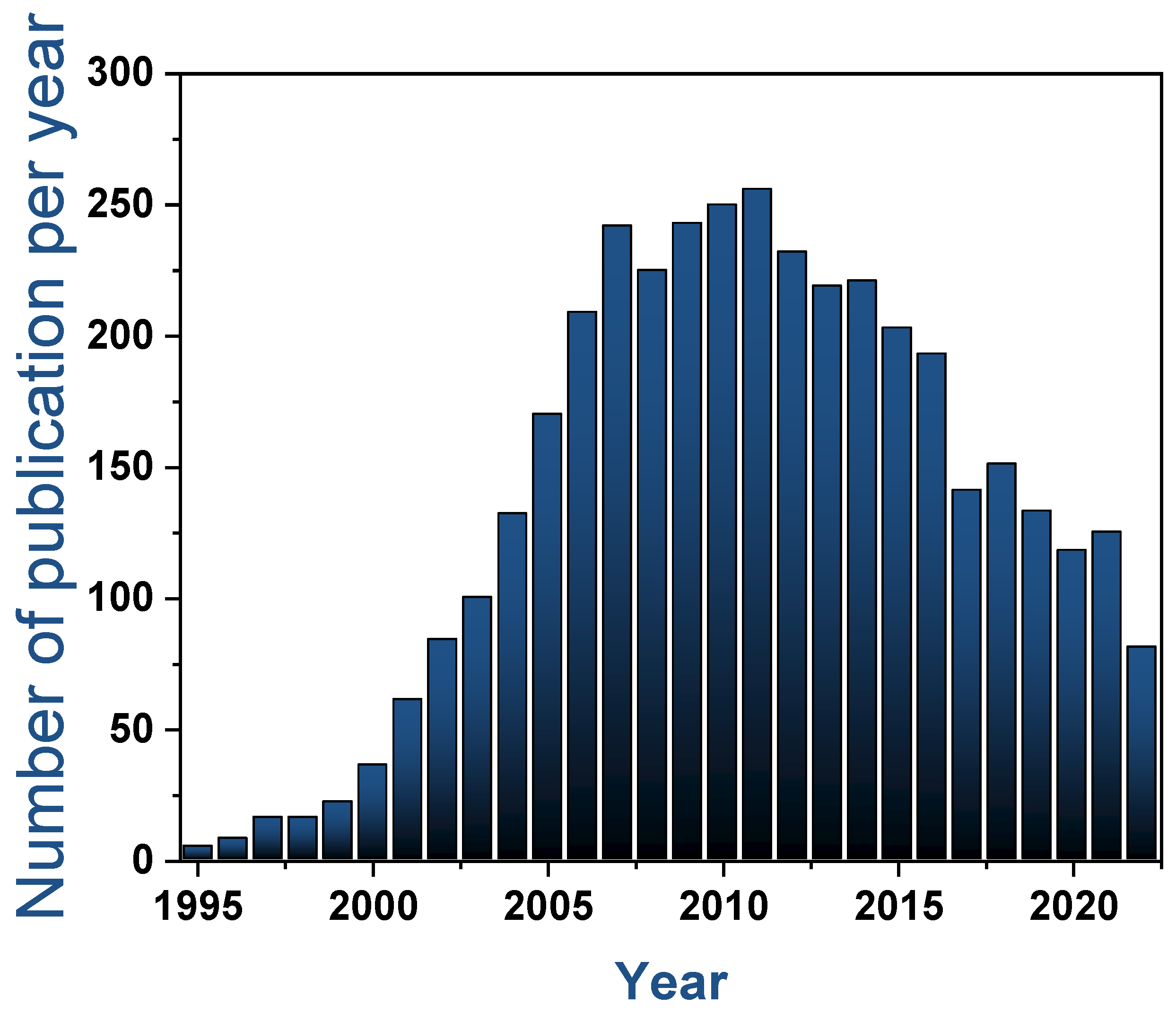
:1. Introduction
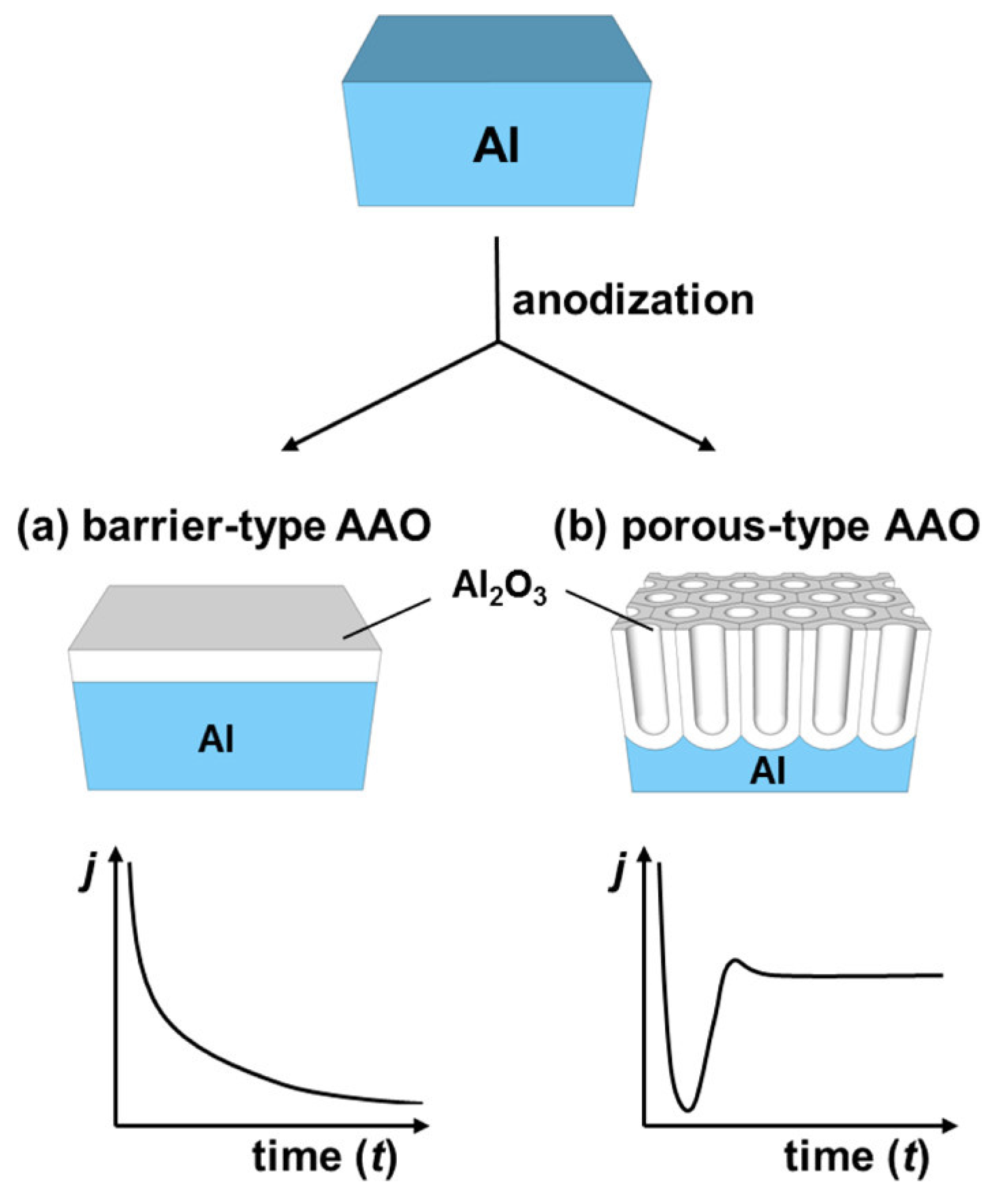
2. Anodized Anodic Alumina
2.1. Types of Anodic Alumina
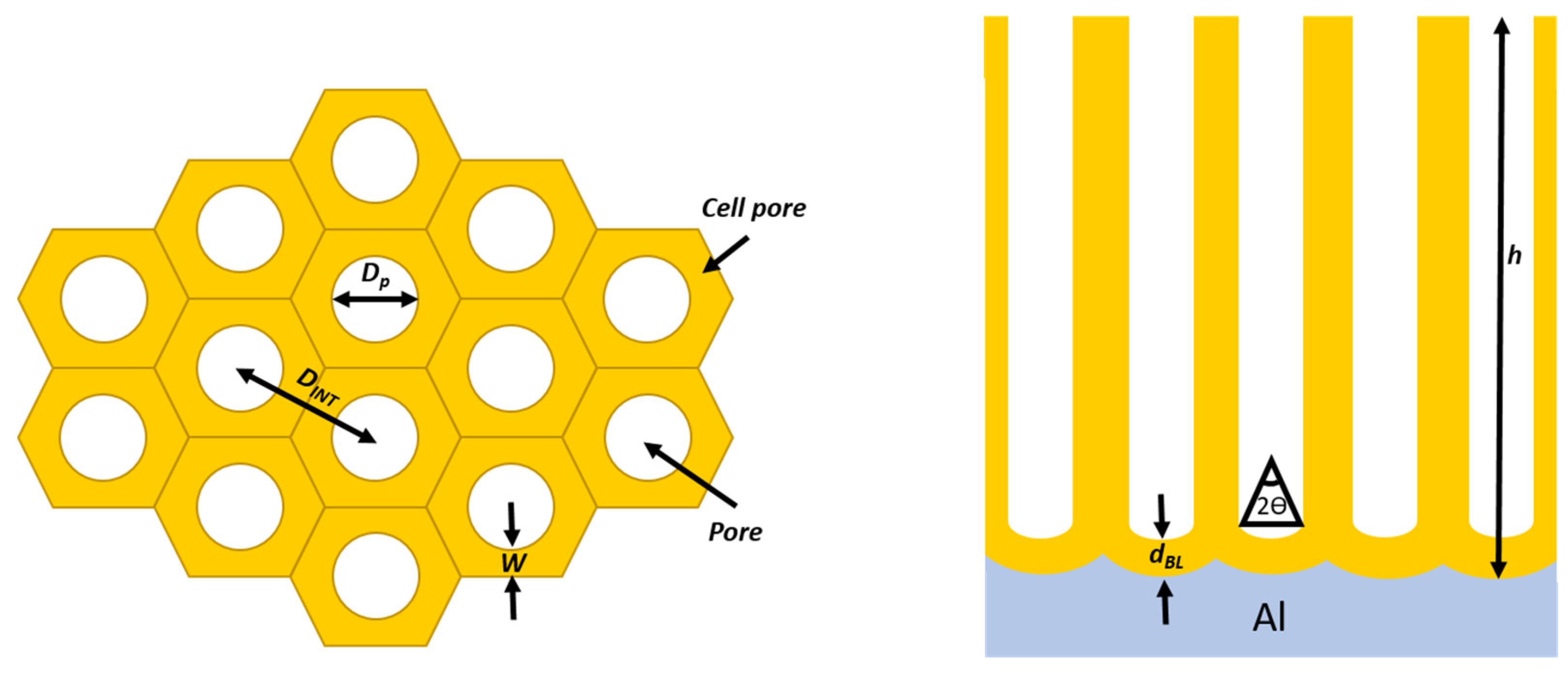
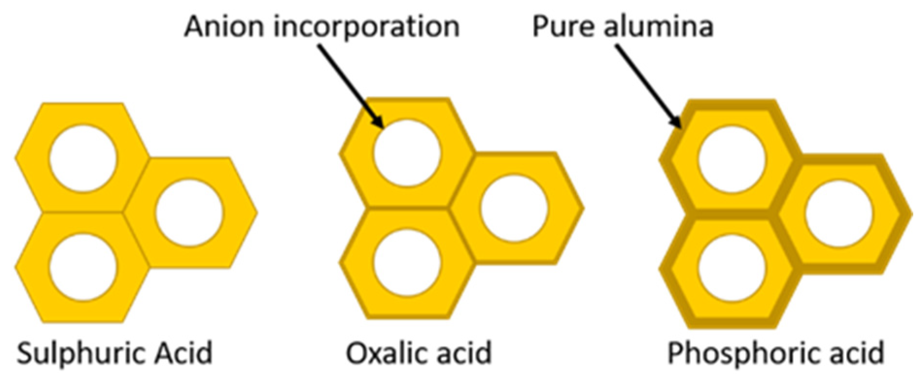
2.2. PAA Templates
2.2.1. Porous Anodic Alumina Formation
2.2.2. PAA Geometrical Features
2.3. Lateral-PAA Template
3. Synthesis of Carbon Nanostructures within PAA Templates
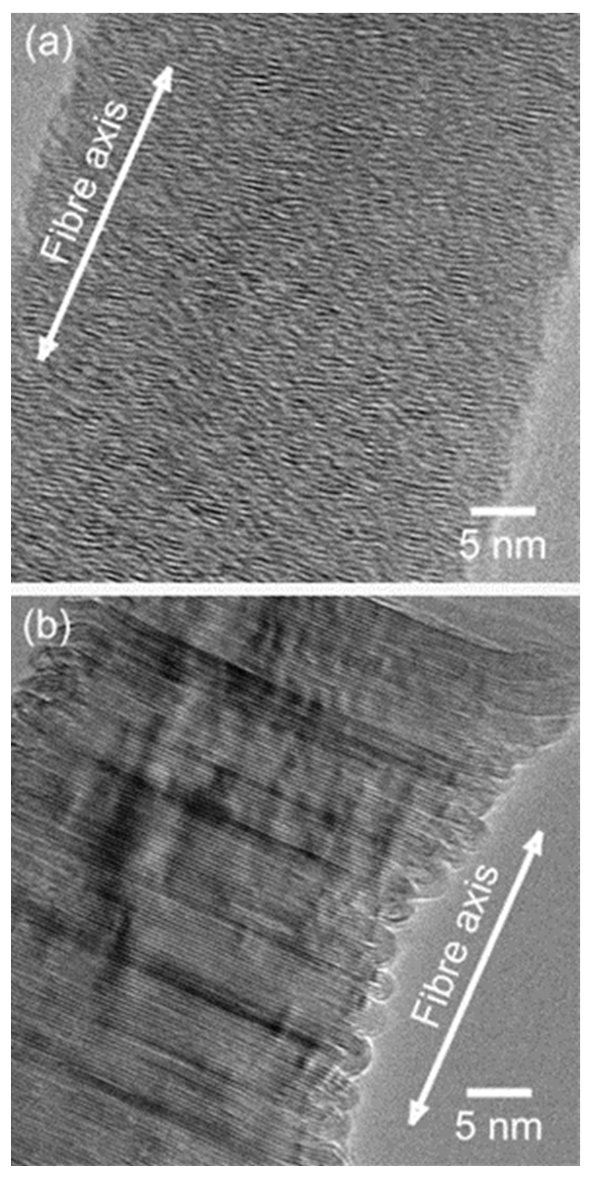
3.1. Carbon Nanotubes (CNTs)
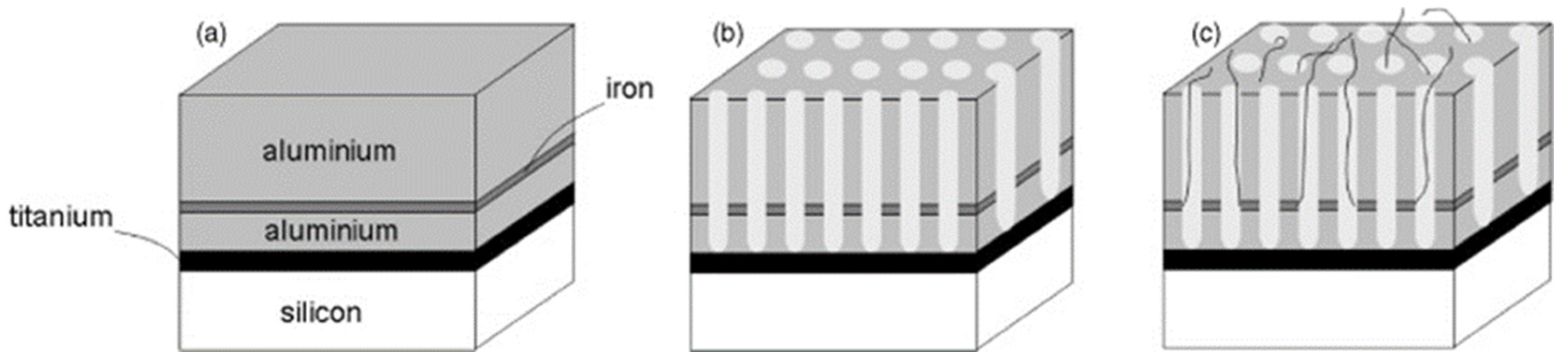
3.1.1. Synthesis of CNTs by the PAA Template Method
3.1.2. Synthesis of CNTs within PAA Templates Using Catalyst NPs
3.2. Graphene and PAA
3.3. Diamond-like Carbon (DLC) and Nanodiamond Synthesis within PAA Templates
3.4. Other Carbon Nanoforms within PAA Templates
4. Applications Based on PAA-Carbon Nanostructures
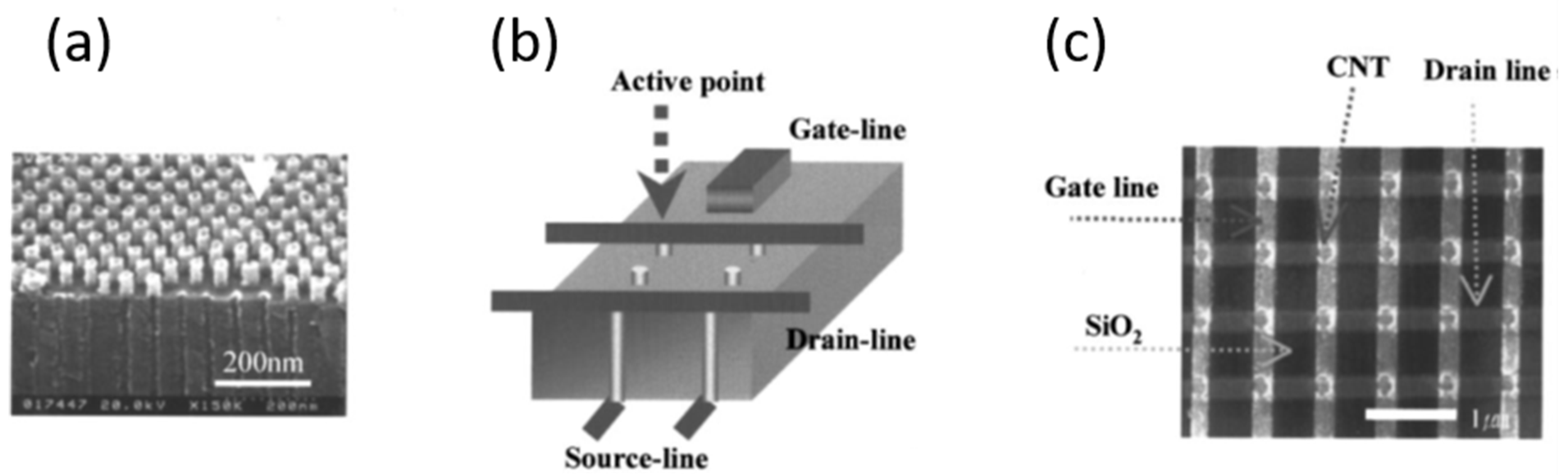
4.1. Electronic Devices Based on PAA/CNTs
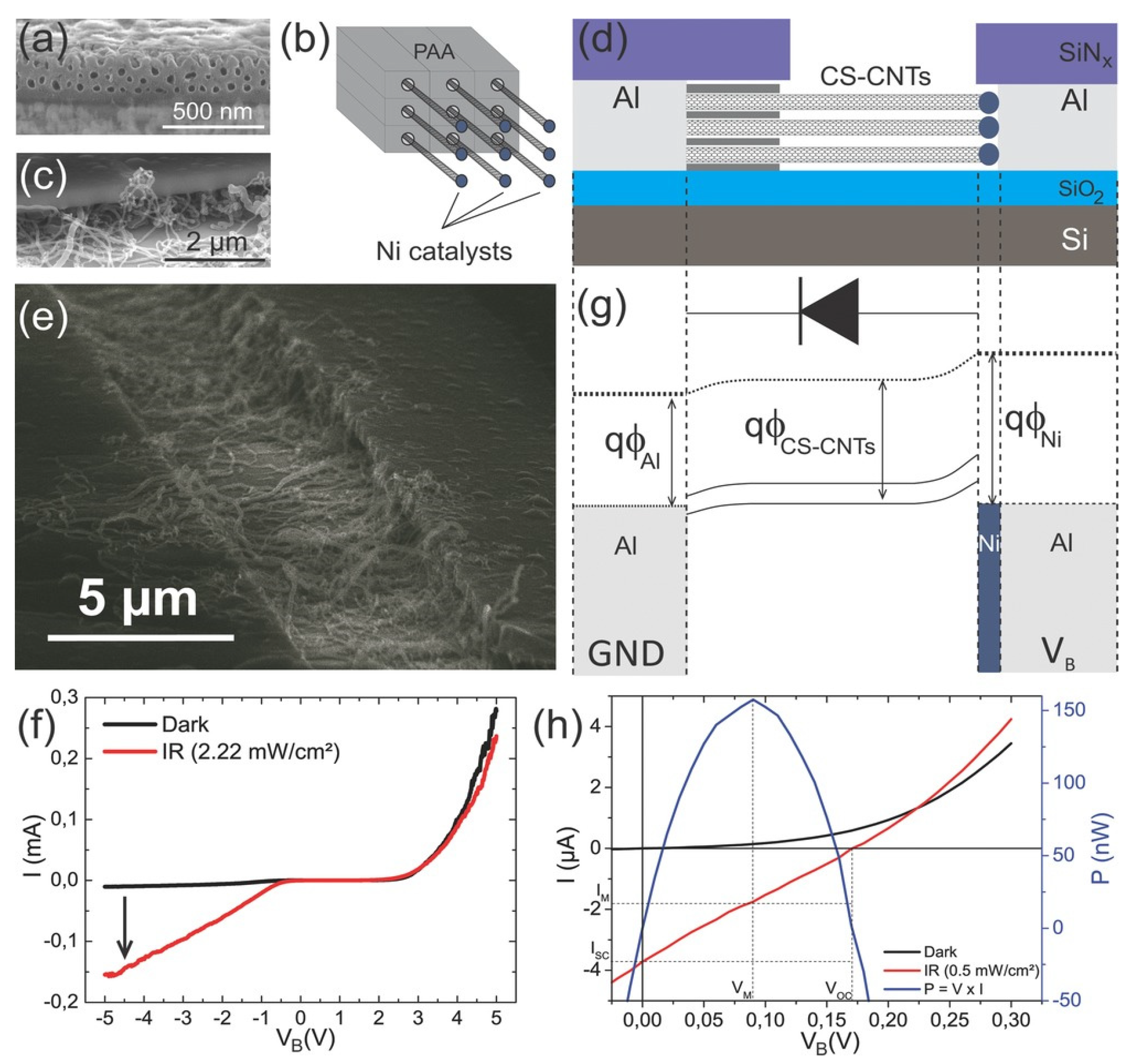
4.2. Energy Conversion and Storage Devices Based on PAA/Carbon Nanostructures Composites
4.3. Molecular Transport within PAA/Carbon Nanostructures
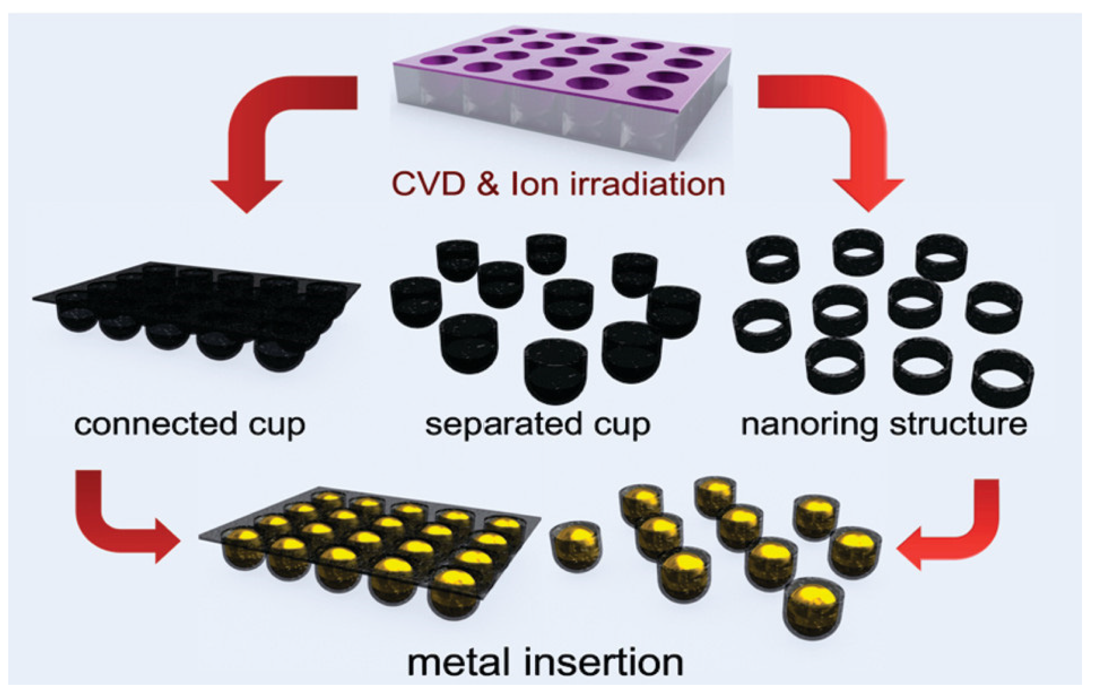
4.4. Photonic Devices Based on Cup-Stacked CNTs Grown inside Lateral-PAA Templates
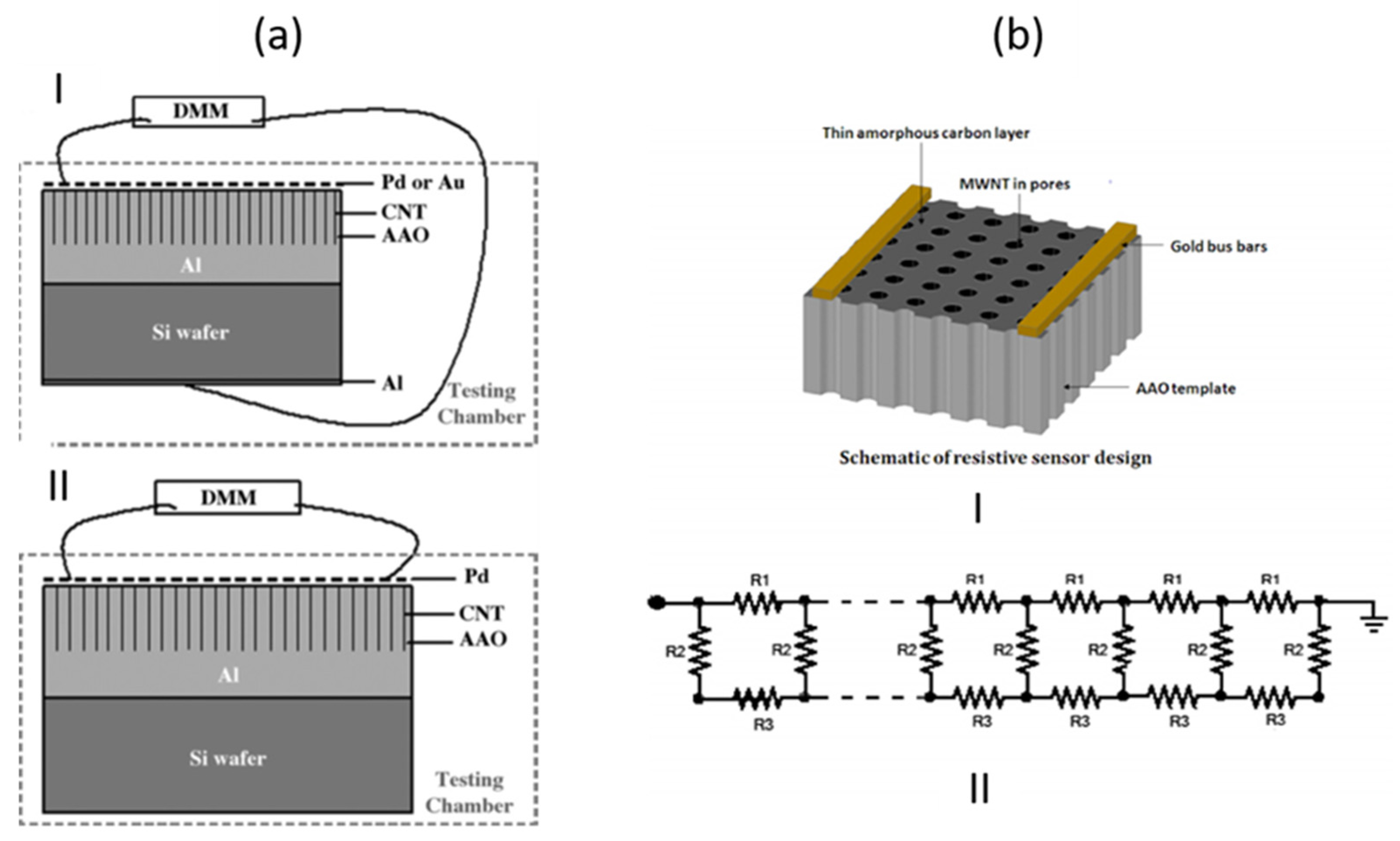
4.5. Gas Sensors Based on PAA/CNTs Devices

4.6. Biosensing and Electrochemical Sensing
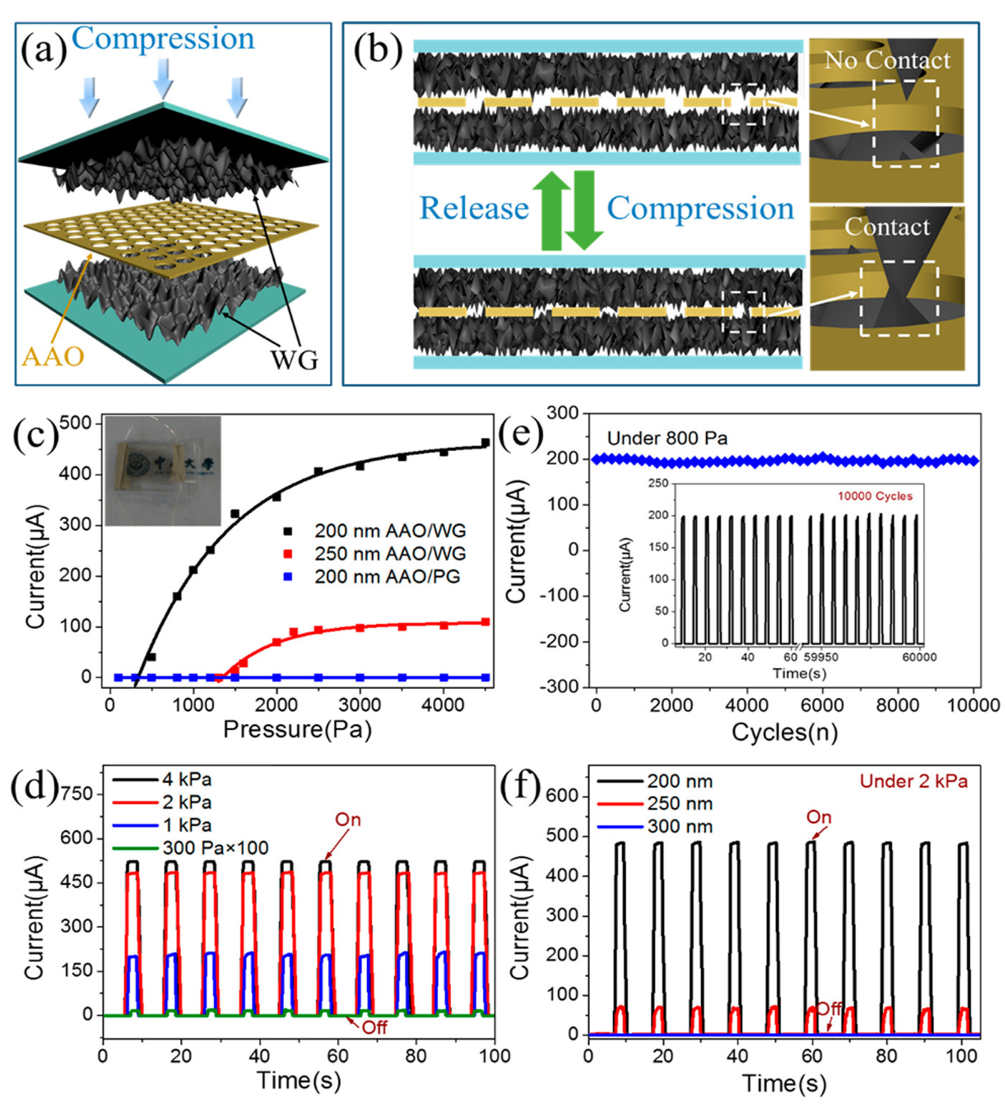
4.7. Pressure Sensor Based on Transferred Wrinkled Graphene
4.8. Composite Materials
5. Final Conclusions and Prospects
Author Contributions
Funding
Institutional Review Board Statement
Informed Consent Statement
Data Availability Statement
Conflicts of Interest
References
- Perevedentseva, E.; Ali, N.; Karmenyan, A.; Skovorodkin, I.; Prunskaite-Hyyryläinen, R.; Vainio, S.; Cheng, C.-L.; Kinnunen, M. Optical Studies of Nanodiamond-Tissue Interaction: Skin Penetration and Localization. Materials 2019, 12, 3762. [Google Scholar] [CrossRef] [PubMed] [Green Version]
- Buron, J.D.; Petersen, D.H.; Bøggild, P.; Cooke, D.G.; Hilke, M.; Sun, J.; Whiteway, E.; Nielsen, P.F.; Hansen, O.; Yurgens, A.; et al. Graphene Conductance Uniformity Mapping. Nano Lett. 2012, 12, 5074–5081. [Google Scholar] [CrossRef] [PubMed]
- Goldsmith, B.R.; Coroneus, J.G.; Khalap, V.R.; Kane, A.A.; Weiss, G.A.; Collins, P.G. Conductance-Controlled Point Functionalization of Single-Walled Carbon Nanotubes. Science 2007, 315, 77–81. [Google Scholar] [CrossRef] [PubMed] [Green Version]
- Felisberto, M.; Tzounis, L.; Sacco, L.; Stamm, M.; Candal, R.; Rubiolo, G.H.; Goyanes, S. Carbon nanotubes grown on carbon fiber yarns by a low temperature CVD method: A significant enhancement of the interfacial adhesion between carbon fiber/epoxy matrix hierarchical composites. Compos. Commun. 2017, 3, 33–37. [Google Scholar] [CrossRef]
- Roman, R.E.; Kwan, K.; Cranford, S.W. Mechanical Properties and Defect Sensitivity of Diamond Nanothreads. Nano Lett. 2015, 15, 1585–1590. [Google Scholar] [CrossRef]
- Che, J.; Çagin, T.; Goddard, W.A. Thermal conductivity of carbon nanotubes. Nanotechnology 2000, 11, 65–69. [Google Scholar] [CrossRef]
- Bressi, V.; Ferlazzo, A.; Iannazzo, D.; Espro, C. Graphene quantum dots by eco-friendly green synthesis for electrochemical sensing: Recent advances and future perspectives. Nanomaterials 2021, 11, 1120. [Google Scholar] [CrossRef]
- Sacco, L.; Forel, S.; Florea, I.; Cojocaru, C.S. Ultra-sensitive NO2 gas sensors based on single-wall carbon nanotube field effect transistors: Monitoring from ppm to ppb level. Carbon 2020, 157, 631–639. [Google Scholar] [CrossRef] [Green Version]
- Maze, J.R.; Stanwix, P.L.; Hodges, J.S.; Hong, S.; Taylor, J.M.; Cappellaro, P.; Jiang, L.; Dutt, M.V.G.; Togan, E.; Zibrov, A.S.; et al. Nanoscale magnetic sensing with an individual electronic spin in diamond. Nature 2008, 455, 644–647. [Google Scholar] [CrossRef]
- Dolleman, R.J.; Hsu, M.; Vollebregt, S.; Sader, J.E.; van der Zant, H.S.J.; Steeneken, P.G.; Ghatkesar, M.K. Mass measurement of graphene using quartz crystal microbalances. Appl. Phys. Lett. 2019, 115, 53102. [Google Scholar] [CrossRef]
- Maschmann, M.R.; Franklin, A.D.; Amama, P.B.; Zakharov, D.N.; Stach, E.A.; Sands, T.D.; Fisher, T.S. Vertical single- and double-walled carbon nanotubes grown from modified porous anodic alumina templates. Nanotechnology 2006, 17, 3925–3929. [Google Scholar] [CrossRef] [Green Version]
- Li, C.; Yang, J.; Zhang, L.; Li, S.; Yuan, Y.; Xiao, X.; Fan, X.; Song, C. Carbon-based membrane materials and applications in water and wastewater treatment: A review. Environ. Chem. Lett. 2021, 19, 1457–1475. [Google Scholar] [CrossRef]
- Li, J.-C.; Hou, P.-X.; Liu, C. Heteroatom-Doped Carbon Nanotube and Graphene-Based Electrocatalysts for Oxygen Reduction Reaction. Small 2017, 13, 1702002. [Google Scholar] [CrossRef] [PubMed] [Green Version]
- Kim, K.H.; Brunel, D.; Gohier, A.; Sacco, L.; Châtelet, M.; Cojocaru, C.S. Cup-stacked carbon nanotube schottky diodes for photovoltaics and photodetectors. Adv. Mater. 2014, 26, 4363–4369. [Google Scholar] [CrossRef]
- Zhong, M.; Zhang, M.; Li, X. Carbon nanomaterials and their composites for supercapacitors. Carbon Energy 2022, 4, 950–985. [Google Scholar] [CrossRef]
- Wang, Y.; Lv, F.; Chen, J.; Huang, Y.; He, S.; Xu, W.; Xu, S.; Wang, W. Evolution of High Symmetry Points of Photonic Alumina Superlattices in a Lithography-Free Approach. ACS Appl. Mater. Interfaces 2021, 13, 47262–47271. [Google Scholar] [CrossRef]
- Meng, F.-L.; Wang, Z.-L.; Zhong, H.-X.; Wang, J.; Yan, J.-M.; Zhang, X.-B. Reactive Multifunctional Template-Induced Preparation of Fe-N-Doped Mesoporous Carbon Microspheres Towards Highly Efficient Electrocatalysts for Oxygen Reduction. Adv. Mater. 2016, 28, 7948–7955. [Google Scholar] [CrossRef]
- Yuan, H.; Zvonkina, I.J.; Al-Enizi, A.M.; Elzatahry, A.A.; Pyun, J.; Karim, A. Facile Assembly of Aligned Magnetic Nanoparticle Chains in Polymer Nanocomposite Films by Magnetic Flow Coating. ACS Appl. Mater. Interfaces 2017, 9, 11290–11298. [Google Scholar] [CrossRef]
- Ma, S.; Tang, Z.; Fan, Y.; Zhao, J.; Meng, X.; Yang, N.; Zhuo, S.; Liu, S. Surfactant-modified graphene oxide membranes with tunable structure for gas separation. Carbon 2019, 152, 144–150. [Google Scholar] [CrossRef]
- Azimi, S.; Dang, Z.; Zhang, C.; Song, J.; Breese, M.B.H.; Sow, C.H.; van Kan, J.A.; van der Maarel, J.R.C. Buried centimeter-long micro- and nanochannel arrays in porous silicon and glass. Lab. A Chip. 2014, 14, 2081–2089. [Google Scholar] [CrossRef]
- Cui, Y.; Duan, W.; Jin, Y.; Wo, F.; Xi, F.; Wu, J. Graphene quantum dot-decorated luminescent porous silicon dressing for theranostics of diabetic wounds. Acta Biomater. 2021, 131, 544–554. [Google Scholar] [CrossRef] [PubMed]
- Eswaramoorthi, I.; Hwang, L.-P. Anodic titanium oxide: A new template for the synthesis of larger diameter multi-walled carbon nanotubes. Diam. Relat. Mater. 2007, 16, 1571–1578. [Google Scholar] [CrossRef]
- Han, Q.; Wang, C.; Chen, H.; Zhao, X.; Wang, J. Porous Tantalum and Titanium in Orthopedics: A Review. ACS Biomater. Sci. Eng. 2019, 5, 5798–5824. [Google Scholar] [CrossRef]
- Apolinário, A.; Sousa, C.T.; Oliveira, G.N.; Lopes, A.M.; Ventura, J.; Andrade, L.; Mendes, A.; Araújo, J.P. Tailoring the anodic hafnium oxide morphology using different organic solvent electrolytes. Nanomaterials 2020, 10, 382. [Google Scholar] [CrossRef] [Green Version]
- Stepniowski, W.J.; Misiolek, W.Z. Review of fabrication methods, physical properties, and applications of nanostructured copper oxides formed via electrochemical oxidation. Nanomaterials 2018, 8, 379. [Google Scholar] [CrossRef] [PubMed] [Green Version]
- Che, G.; Lakshmi, B.B.; Martin, C.R.; Fisher, E.R.; Ruoff, R.S. Chemical Vapor Deposition Based Synthesis of Carbon Nanotubes and Nanofibers Using a Template Method. Chem. Mater. 1998, 10, 260–267. [Google Scholar] [CrossRef]
- Zhou, Z.; Nonnenmann, S.S. Progress in Nanoporous Templates: Beyond Anodic Aluminum Oxide and Towards Functional Complex Materials. Materials 2019, 12, 2535. [Google Scholar] [CrossRef] [Green Version]
- Alsawat, M.; Altalhi, T.; Santos, A.; Losic, D. Carbon Nanotubes–Nanoporous Anodic Alumina Composite Membranes: Influence of Template on Structural, Chemical, and Transport Properties. J. Phys. Chem. C 2017, 121, 13634–13644. [Google Scholar] [CrossRef]
- Stępniowski, W.J.; Moneta, M.; Norek, M.; Michalska-Domańska, M.; Scarpellini, A.; Salerno, M. The influence of electrolyte composition on the growth of nanoporous anodic alumina. Electrochim. Acta 2016, 211, 453–460. [Google Scholar] [CrossRef]
- Lee, W.; Park, S.J. Porous anodic aluminum oxide: Anodization and templated synthesis of functional nanostructures. Chem. Rev. 2014, 114, 7487–7556. [Google Scholar] [CrossRef]
- Resende, P.M.; Martín-González, M. Sub-10 nm porous alumina templates to produce sub-10 nm nanowires. Microporous Mesoporous Mater. 2019, 284, 198–204. [Google Scholar] [CrossRef]
- Bendova, M.; Kolar, J.; Gispert-Guirado, F.; Mozalev, A. Porous-Alumina-Assisted Growth of Nanostructured Anodic Films on Ti−Nb Alloys. ChemElectroChem 2018, 5, 2825–2835. [Google Scholar] [CrossRef]
- Mozalev, A.; Hubalek, J. On-substrate porous-anodic-alumina-assisted gold nanostructure arrays: Meeting the challenges of various sizes and interfaces. Electrochim. Acta 2019, 297, 988–999. [Google Scholar] [CrossRef]
- Zamrik, I.; Bayat, H.; Alhusaini, Q.; Raoufi, M.; Schönherr, H. In situ Study of Layer by Layer Polyelectrolyte Deposition in Nanopores of Anodic Aluminum Oxide by Reflectometric Interference Spectroscopy. Langmuir 2020, 36, 1907–1915. [Google Scholar] [CrossRef] [PubMed]
- Nakajima, D.; Kikuchi, T.; Yoshioka, T.; Matsushima, H.; Ueda, M.; Suzuki, R.O.; Natsui, S. A Superhydrophilic Aluminum Surface with Fast Water Evaporation Based on Anodic Alumina Bundle Structures via Anodizing in Pyrophosphoric Acid. Materials 2019, 12, 3497. [Google Scholar] [CrossRef] [Green Version]
- Kandy, M.M.; Gaikar, V.G. Enhanced photocatalytic reduction of CO2 using CdS/Mn2O3 nanocomposite photocatalysts on porous anodic alumina support with solar concentrators. Renew. Energy 2019, 139, 915–923. [Google Scholar] [CrossRef]
- Lagrichi, O.; Morin, A.; Buttard, D. Platinum-Nickel Nanotubes Array as Cathode for PEMFC. ECS Trans. 2019, 92, 627–633. [Google Scholar] [CrossRef]
- Liu, S.; Tian, J.; Zhang, W. Fabrication and application of nanoporous anodic aluminum oxide: A review. Nanotechnology 2021, 32, 222001. [Google Scholar] [CrossRef]
- Choudhari, K.S.; Choi, C.-H.; Chidangil, S.; George, S.D. Recent Progress in the Fabrication and Optical Properties of Nanoporous Anodic Alumina. Nanomaterials 2022, 12, 444. [Google Scholar] [CrossRef]
- Manzoor, S.; Ashraf, M.W.; Tayyaba, S.; Hossain, M.K. Recent progress of fabrication, characterization, and applications of anodic aluminum oxide (AAO) membrane: A review. arXiv 2021, arXiv:2112.08450. [Google Scholar] [CrossRef]
- Li, C.; Ni, Y.; Gong, J.; Song, Y.; Gong, T.; Zhu, X. A review: Research progress on the formation mechanism of porous anodic oxides. Nanoscale Adv. 2022, 4, 322–333. [Google Scholar] [CrossRef]
- Pashchanka, M. Conceptual progress for explaining and predicting self-organization on anodized aluminum surfaces. Nanomaterials 2021, 11, 2271. [Google Scholar] [CrossRef] [PubMed]
- Ruiz-Clavijo, A.; Caballero-Calero, O.; Martín-González, M. Revisiting anodic alumina templates: From fabrication to applications. Nanoscale 2021, 13, 2227–2265. [Google Scholar] [CrossRef] [PubMed]
- Domagalski, J.T.; Xifre-Perez, E.; Marsal, L.F. Recent advances in nanoporous anodic alumina: Principles, engineering, and applications. Nanomaterials 2021, 11, 430. [Google Scholar] [CrossRef] [PubMed]
- Gorisse, T.; Dupré, L.; Zelsmann, M.; Vlad, A.; Coati, A.; Garreau, Y.; Buttard, D. In Situ Investigation of the Early-Stage Growth of Nanoporous Alumina. J. Nanomater. 2018, 2018, 6428271. [Google Scholar] [CrossRef] [Green Version]
- Evertsson, J.; Vinogradov, N.A.; Harlow, G.S.; Carlà, F.; McKibbin, S.R.; Rullik, L.; Linpé, W.; Felici, R.; Lundgren, E. Self-organization of porous anodic alumina films studied in situ by grazing-incidence transmission small-angle X-ray scattering. RSC Adv. 2018, 8, 18980–18991. [Google Scholar] [CrossRef] [Green Version]
- Linpé, W.; Harlow, G.S.; Evertsson, J.; Hejral, U.; Abbondanza, G.; Lenrick, F.; Seifert, S.; Felici, R.; Vinogradov, N.A.; Lundgren, E. The State of Electrodeposited Sn Nanopillars within Porous Anodic Alumina from in Situ X-ray Observations. ACS Appl. Nano Mater. 2019, 2, 3031–3038. [Google Scholar] [CrossRef]
- Vinogradov, N.A.; Harlow, G.S.; Carlà, F.; Evertsson, J.; Rullik, L.; Linpé, W.; Felici, R.; Lundgren, E. Observation of Pore Growth and Self-Organization in Anodic Alumina by Time-Resolved X-ray Scattering. ACS Appl. Nano Mater. 2018, 1, 1265–1271. [Google Scholar] [CrossRef]
- Heinschke, S.; Schneider, J.J. On the Prediction of Well-Ordered Porous Anodic Alumina Films. J. Phys. Chem. C 2020, 124, 11913–11921. [Google Scholar] [CrossRef]
- Lv, Y. Research progress in formation mechanism of anodizing aluminum oxide. In Proceedings of the IOP Conference Series: Earth and Environmental Science, Sanya, China, 20–22 November 2017; IOP Publishing: Bristol, UK, 2017; Volume 100, p. 12022. [Google Scholar] [CrossRef]
- Keller, F.; Hunter, M.S.; Robinson, D.L. Structural features of oxide coatings on aluminum. J. Electrochem. Soc. 1953, 100, 411–419. [Google Scholar] [CrossRef]
- O’Sullivan, J.P.; Wood, G.C. The Morphology and Mechanism of Formation of Porous Anodic Films on Aluminium. Proc. R. Soc. A Math. Phys. Eng. Sci. 1970, 317, 511–543. [Google Scholar] [CrossRef]
- Masuda, H.; Fukuda, K. Ordered Metal Nanohole Arrays Made by a Two-Step Replication of Honeycomb Structures of Anodic Alumina. Science 1995, 268, 1466–1468. [Google Scholar] [CrossRef] [PubMed]
- Li, A.P.; Müller, F.; Birner, A.; Nielsch, K.; Gösele, U. Hexagonal pore arrays with a 50–420 nm interpore distance formed by self-organization in anodic alumina. J. Appl. Phys. 1998, 84, 6023–6026. [Google Scholar] [CrossRef] [Green Version]
- Stępniowski, W.J.; Norek, M.; Michalska-Domańska, M.; Bojar, Z. Ultra-small nanopores obtained by self-organized anodization of aluminum in oxalic acid at low voltages. Mater. Lett. 2013, 111, 20–23. [Google Scholar] [CrossRef]
- Runge, J.M. The Metallurgy of Anodizing Aluminum; Springer: Berlin/Heidelberg, Germany, 2017. [Google Scholar]
- Yao, M.; Chen, J.; Su, Z.; Peng, Y.; Li, F.; Yao, X. Ionic transport and barrier effect of anodic oxide layer in a solid-state Al2O3 capacitor under high electric field. Electrochim. Acta 2017, 224, 235–242. [Google Scholar] [CrossRef] [Green Version]
- Cancellieri, C.; Evangelisti, F.; Geldmacher, T.; Araullo-Peters, V.; Ott, N.; Chiodi, M.; Döbeli, M.; Schmutz, P. The role of Si incorporation on the anodic growth of barrier-type Al oxide. Mater. Sci. Eng. B 2017, 226, 120–131. [Google Scholar] [CrossRef]
- Chen, J.; Yao, M.; Xiao, R.; Yang, P.; Hu, B.; Yao, X. The application of the barrier-type anodic oxidation method to thickness testing of aluminum films. Rev. Sci. Instrum. 2014, 85, 94101. [Google Scholar] [CrossRef]
- Evangelisti, F.; Stiefel, M.; Guseva, O.; Partovi Nia, R.; Hauert, R.; Hack, E.; Jeurgens, L.P.H.; Ambrosio, F.; Pasquarello, A.; Schmutz, P.; et al. Electronic and structural characterization of barrier-type amorphous aluminium oxide. Electrochim. Acta 2017, 224, 503–516. [Google Scholar] [CrossRef]
- González-Castaño, M.; Cancellieri, C.; Maeder, X.; Hack, E.; Schmutz, P. Enhancing the insulating and dielectric properties of barrier anodic Al2O3 on high purity aluminum. Appl. Surf. Sci. 2020, 505, 144522. [Google Scholar] [CrossRef]
- Ide, S.; Capraz, Ö.Ö.; Shrotriya, P.; Hebert, K.R. Oxide Microstructural Changes Accompanying Pore Formation during Anodic Oxidation of Aluminum. Electrochim. Acta 2017, 232, 303–309. [Google Scholar] [CrossRef]
- Thompson, G.E. Porous anodic alumina: Fabrication, characterization and applications. Thin Solid Film. 1997, 297, 192–201. [Google Scholar] [CrossRef]
- Nielsch, K.; Choi, J.; Schwirn, K.; Wehrspohn, R.B.; Gösele, U. Self-ordering Regimes of Porous Alumina: The 10 Porosity Rule. Nano Lett. 2002, 2, 677–680. [Google Scholar] [CrossRef]
- Thompson, G.E.; Furneaux, R.C.; Wood, G.C.; Richardson, J.A.; Goode, J.S. Nucleation and growth of porous anodic films on aluminium. Nature 1978, 272, 433–435. [Google Scholar] [CrossRef]
- Patermarakis, G. The origin of nucleation and development of porous nanostructure of anodic alumina films. J. Electroanal. Chem. 2009, 635, 39–50. [Google Scholar] [CrossRef]
- Hebert, K.R.; Albu, S.P.; Paramasivam, I.; Schmuki, P. Morphological instability leading to formation of porous anodic oxide films. Nat. Mater. 2012, 11, 162–166. [Google Scholar] [CrossRef]
- Sui, Y.C.; Cui, B.Z.; Martínez, L.; Perez, R.; Sellmyer, D.J. Pore structure, barrier layer topography and matrix alumina structure of porous anodic alumina film. Thin Solid Film. 2002, 406, 64–69. [Google Scholar] [CrossRef] [Green Version]
- Houser, J.E.; Hebert, K.R. The role of viscous flow of oxide in the growth of self-ordered porous anodic alumina films. Nat. Mater. 2009, 8, 415–420. [Google Scholar] [CrossRef]
- Garcia-Vergara, S.J.; Skeldon, P.; Thompson, G.E.; Habazaki, H. A flow model of porous anodic film growth on aluminium. Electrochim. Acta 2006, 52, 681–687. [Google Scholar] [CrossRef]
- Su, Z.; Hähner, G.; Zhou, W. Investigation of the pore formation in anodic aluminium oxide. J. Mater. Chem. 2008, 18, 5787–5795. [Google Scholar] [CrossRef]
- Mirzoev, R.A.; Davydov, A.D.; Vystupov, S.I.; Kabanova, T.B. Conditions for self-ordering of porous structure of anodic aluminum oxide in weak and strong acids. Electrochim. Acta 2019, 294, 276–285. [Google Scholar] [CrossRef]
- Pashchanka, M.; Schneider, J.J. Origin of self-organisation in porous anodic alumina films derived from analogy with Rayleigh–Bénard convection cells. J. Mater. Chem. 2011, 21, 18761–18767. [Google Scholar] [CrossRef]
- Roslyakov, I.V.; Gordeeva, E.O.; Napolskii, K.S. Role of Electrode Reaction Kinetics in Self-Ordering of Porous Anodic Alumina. Electrochim. Acta 2017, 241, 362–369. [Google Scholar] [CrossRef]
- Napolskii, K.S.; Roslyakov, I.V.; Eliseev, A.A.; Byelov, D.V.; Petukhov, A.V.; Grigoryeva, N.A.; Bouwman, W.G.; Lukashin, A.V.; Chumakov, A.P.; Grigoriev, S.V. The Kinetics and Mechanism of Long-Range Pore Ordering in Anodic Films on Aluminum. J. Phys. Chem. C 2011, 115, 23726–23731. [Google Scholar] [CrossRef]
- Mercier, D.; Van Overmeere, Q.; Santoro, R.; Proost, J. In-situ optical emission spectrometry during galvanostatic aluminum anodising. Electrochim. Acta 2011, 56, 1329–1336. [Google Scholar] [CrossRef]
- Veys-Renaux, D.; Chahboun, N.; Rocca, E. Anodizing of multiphase aluminium alloys in sulfuric acid: In-situ electrochemical behaviour and oxide properties. Electrochim. Acta 2016, 211, 1056–1065. [Google Scholar] [CrossRef]
- Kim, H.; Lee, J.T.; Magasinski, A.; Zhao, K.; Liu, Y.; Yushin, G. In Situ TEM Observation of Electrochemical Lithiation of Sulfur Confined within Inner Cylindrical Pores of Carbon Nanotubes. Adv. Energy Mater. 2015, 5, 1501306. [Google Scholar] [CrossRef]
- Huang, X.; Farra, R.; Schlögl, R.; Willinger, M.-G. Growth and Termination Dynamics of Multiwalled Carbon Nanotubes at Near Ambient Pressure: An in Situ Transmission Electron Microscopy Study. Nano Lett. 2019, 19, 5380–5387. [Google Scholar] [CrossRef] [Green Version]
- Bremmer, G.M.; Zacharaki, E.; Sjåstad, A.O.; Navarro, V.; Frenken, J.W.M.; Kooyman, P.J. In situ TEM observation of the Boudouard reaction: Multi-layered graphene formation from CO on cobalt nanoparticles at atmospheric pressure. Faraday Discuss. 2017, 197, 337–351. [Google Scholar] [CrossRef] [Green Version]
- Shiryaev, A.A.; Hinks, J.; Marks, N.; Greaves, G.; Donnelly, S.; Fisenko, A.V.; Kiwi, M. Xenon Implantation in Nanodiamonds: In Situ Transmission Electron Microscopy Study and Molecular Dynamics Simulations. In Proceedings of the 79th Annual Meeting of the Meteoritical Society, Berlin, Germany, 7–12 August 2016. [Google Scholar]
- Huang, X.; Mutlu, H.; Théato, P. The toolbox of porous anodic aluminum oxide–based nanocomposites: From preparation to application. Colloid Polym. Sci. 2020, 299, 325–341. [Google Scholar] [CrossRef]
- Sacco, L.; Florea, I.; Châtelet, M.; Cojocaru, C.-S. Electrical and morphological behavior of carbon nanotubes synthesized within porous anodic alumina templates. J. Phys. Mater. 2018, 1, 015004. [Google Scholar] [CrossRef] [Green Version]
- Stępniowski, W.J.; Bojar, Z. Synthesis of anodic aluminum oxide (AAO) at relatively high temperatures. Study of the influence of anodization conditions on the alumina structural features. Surf. Coat. Technol. 2011, 206, 265–272. [Google Scholar] [CrossRef]
- Reddy, P.R.; Ajith, K.M.; Udayashankar, N.K. Morphology and photoluminescence of nano-porous anodic alumina membranes obtained in oxalic acid at different anodization potentials. Nano Express 2020, 1, 10047. [Google Scholar] [CrossRef]
- Zaraska, L.; Sulka, G.D.; Jaskuła, M. The effect of n-alcohols on porous anodic alumina formed by self-organized two-step anodizing of aluminum in phosphoric acid. Surf. Coat. Technol. 2010, 204, 1729–1737. [Google Scholar] [CrossRef]
- Yi, L.; Zhiyuan, L.; Xing, H.; Yisen, L.; Yi, C. Investigation of intrinsic mechanisms of aluminium anodization processes by analyzing the current density. RSC Adv. 2012, 2, 5164–5171. [Google Scholar] [CrossRef]
- Zaraska, L.; Sulka, G.D.; Jaskuła, M. Porous anodic alumina membranes formed by anodization of AA1050 alloy as templates for fabrication of metallic nanowire arrays. Surf. Coat. Technol. 2010, 205, 2432–2437. [Google Scholar] [CrossRef]
- Friedman, A.L.; Brittain, D.; Menon, L. Roles of pH and acid type in the anodic growth of porous alumina. J. Chem. Phys. 2007, 127, 154717. [Google Scholar] [CrossRef]
- Lee, W.; Ji, R.; Gösele, U.; Nielsch, K. Fast fabrication of long-range ordered porous alumina membranes by hard anodization. Nat. Mater. 2006, 5, 741–747. [Google Scholar] [CrossRef]
- Li, Y.; Zheng, M.; Ma, L.; Shen, W. Fabrication of highly ordered nanoporous alumina films by stable high-field anodization. Nanotechnology 2006, 17, 5101–5105. [Google Scholar] [CrossRef]
- Lozovenko, A.A.; Poznyak, A.A.; Gorokh, G.G. Synthesis of bismuth nanowires for thermoelectric applications. J. Phys. Conf. Ser. 2018, 1124, 22013. [Google Scholar] [CrossRef]
- Stepniowski, W.J.; Moneta, M.; Karczewski, K.; Michalska-Domanska, M.; Czujko, T.; Mol, J.M.C.; Buijnsters, J.G. Fabrication of copper nanowires via electrodeposition in anodic aluminum oxide templates formed by combined hard anodizing and electrochemical barrier layer thinning. J. Electroanal. Chem. 2018, 809, 59–66. [Google Scholar] [CrossRef] [Green Version]
- Mozalev, A.; Magaino, S.; Imai, H. The formation of nanoporous membranes from anodically oxidized aluminium and their application to Li rechargeable batteries. Electrochim. Acta 2001, 46, 2825–2834. [Google Scholar] [CrossRef]
- Santos, A.; Vojkuvka, L.; Pallarés, J.; Ferré-Borrull, J.; Marsal, L.F. In situ electrochemical dissolution of the oxide barrier layer of porous anodic alumina fabricated by hard anodization. J. Electroanal. Chem. 2009, 632, 139–142. [Google Scholar] [CrossRef]
- Furneaux, R.C.; Rigby, W.R.; Davidson, A.P. The formation of controlled-porosity membranes from anodically oxidized aluminium. Nature 1989, 337, 147–149. [Google Scholar] [CrossRef]
- Lillo, M.; Losic, D. Pore opening detection for controlled dissolution of barrier oxide layer and fabrication of nanoporous alumina with through-hole morphology. J. Membr. Sci. 2009, 327, 11–17. [Google Scholar] [CrossRef]
- Ba, L.; Li, W.S. Influence of anodizing conditions on the ordered pore formation in anodic alumina. J. Phys. D Appl. Phys. 2000, 33, 2527–2531. [Google Scholar] [CrossRef]
- Lillo, M.; Losic, D. Ion-beam pore opening of porous anodic alumina: The formation of single nanopore and nanopore arrays. Mater. Lett. 2009, 63, 457–460. [Google Scholar] [CrossRef]
- Sacco, L.; Florea, I.; Cojocaru, C.-S. Fabrication of porous anodic alumina (PAA) templates with straight pores and with hierarchical structures through exponential voltage decrease technique. Surf. Coat. Technol. 2019, 364, 248–255. [Google Scholar] [CrossRef] [Green Version]
- Abd-Elnaiem, A.M.; Gaber, A. Parametric study on the anodization of pure aluminum thin film used in fabricating nano-pores template. Int. J. Electrochem. Sci. 2013, 8, 9741–9751. [Google Scholar]
- Stępniowski, W.J.; Florkiewicz, W.; Michalska-Domańska, M.; Norek, M.; Czujko, T. A comparative study of electrochemical barrier layer thinning for anodic aluminum oxide grown on technical purity aluminum. J. Electroanal. Chem. 2015, 741, 80–86. [Google Scholar] [CrossRef]
- Sheasby, P.G.; Wernick, S.; Pinner, R. Surface Treatment and Finishing of Aluminum and Its Alloys; ASM International: Geauga, OH, USA, 1987; Volumes 1 and 2. [Google Scholar]
- Chong, B.; Yu, D.; Jin, R.; Wang, Y.; Li, D.; Song, Y.; Gao, M.; Zhu, X. Theoretical derivation of anodizing current and comparison between fitted curves and measured curves under different conditions. Nanotechnology 2015, 26, 145603. [Google Scholar] [CrossRef]
- Hunter, M.S.; Fowle, P. Determination of Barrier Layer Thickness of Anodic Oxide Coatings. J. Electrochem. Soc. 1954, 101, 481–485. [Google Scholar] [CrossRef]
- Han, H.; Park, S.-J.; Jang, J.S.; Ryu, H.; Kim, K.J.; Baik, S.; Lee, W. In Situ Determination of the Pore Opening Point during Wet-Chemical Etching of the Barrier Layer of Porous Anodic Aluminum Oxide: Nonuniform Impurity Distribution in Anodic Oxide. ACS Appl. Mater. Interfaces 2013, 5, 3441–3448. [Google Scholar] [CrossRef] [PubMed]
- Li, J.-Y.; Wu, Z.-Q.; Xu, J.-J.; Li, C.-Y.; Chen, H.-Y.; Xia, X.-H. A stochastic route to simulate the growth of porous anodic alumina. RSC Adv. 2014, 4, 45074–45081. [Google Scholar] [CrossRef]
- Sulka, G.D. Highly Ordered Anodic Porous Alumina Formation by Self-Organized Anodizing. In Nanostructured Materials in Electrochemistry; Wiley-VCH: Weinheim, Germany, 2008; Volume 1, pp. 1–116. [Google Scholar]
- Stępniowski, W.J.; Zasada, D.; Bojar, Z. First step of anodization influences the final nanopore arrangement in anodized alumina. Surf. Coat. Technol. 2011, 206, 1416–1422. [Google Scholar] [CrossRef]
- Stępniowski, W.J.; Nowak-Stępniowska, A.; Bojar, Z. Quantitative arrangement analysis of anodic alumina formed by short anodizations in oxalic acid. Mater. Charact. 2013, 78, 79–86. [Google Scholar] [CrossRef]
- Shingubara, S.; Morimoto, K.; Sakaue, H.; Takahagi, T. Self-Organization of a Porous Alumina Nanohole Array Using a Sulfuric/Oxalic Acid Mixture as Electrolyte. Electrochem. Solid-State Lett. 2004, 7, E15–E17. [Google Scholar] [CrossRef]
- Mínguez-Bacho, I.; Rodríguez-López, S.; Asenjo, A.; Vázquez, M.; Hernández-Vélez, M. Self-correlation function for determination of geometrical parameters in Nanoporous Anodic Alumina Films. Appl. Phys. A Mater. Sci. Process. 2012, 106, 105–112. [Google Scholar] [CrossRef]
- Zaraska, L.; Stępniowski, W.J.; Sulka, G.D.; Ciepiela, E.; Jaskuła, M. Analysis of nanopore arrangement and structural features of anodic alumina layers formed by two-step anodizing in oxalic acid using the dedicated executable software. Appl. Phys. A 2014, 114, 571–577. [Google Scholar] [CrossRef] [Green Version]
- Toccafondi, C.; Stȩpniowski, W.J.; Leoncini, M.; Salerno, M. Advanced morphological analysis of patterns of thin anodic porous alumina. Mater. Charact. 2014, 94, 26–36. [Google Scholar] [CrossRef]
- Cojocaru, C.S.; Padovani, J.M.; Wade, T.; Mandoli, C.; Jaskierowicz, G.; Wegrowe, J.E.; i Morral, A.F.; Pribat, D. Conformal Anodic Oxidation of Aluminum Thin Films. Nano Lett. 2005, 5, 675–680. [Google Scholar] [CrossRef]
- Oh, J.; Thompson, C.V. Abnormal Anodic Aluminum Oxide Formation in Confined Structures for Lateral Pore Arrays. J. Electrochem. Soc. 2011, 158, C71. [Google Scholar] [CrossRef]
- Xiang, Y.; Lee, W.; Nielsch, K.; Abstreiter, G.; Fontcuberta i Morral, A. Microstructured horizontal alumina pore arrays as growth templates for large area few and single nanowire devices. Phys. Status Solidi RRL—Rapid Res. Lett. 2008, 2, 59–61. [Google Scholar] [CrossRef]
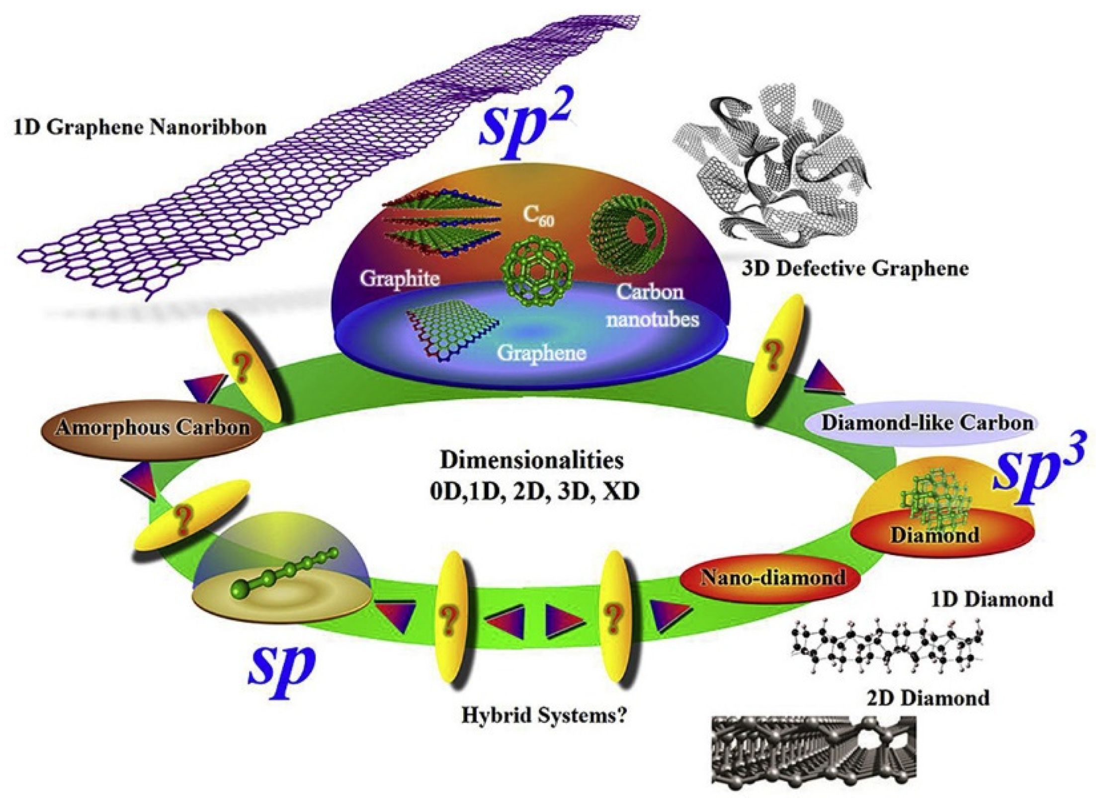
- Bianco, A.; Chen, Y.; Chen, Y.; Ghoshal, D.; Hurt, R.H.; Kim, Y.A.; Koratkar, N.; Meunier, V.; Terrones, M. A carbon science perspective in 2018: Current achievements and future challenges. Carbon 2018, 132, 785–801. [Google Scholar] [CrossRef]
- Nasir, S.; Hussein, Z.M.; Zainal, Z.; Yusof, A.N. Carbon-Based Nanomaterials/Allotropes: A Glimpse of Their Synthesis, Properties and Some Applications. Materials 2018, 11, 295. [Google Scholar] [CrossRef] [PubMed] [Green Version]
- Liu, Y.; Zhan, G.; Wang, Q.; He, D.; Zhang, J.; Liang, A.; Moellendick, T.E.; Zhao, L.; Li, X. Hardness of Polycrystalline Wurtzite Boron Nitride (wBN) Compacts. Sci. Rep. 2019, 9, 10215. [Google Scholar] [CrossRef] [Green Version]
- Georgakilas, V.; Perman, J.A.; Tucek, J.; Zboril, R. Broad Family of Carbon Nanoallotropes: Classification, Chemistry, and Applications of Fullerenes, Carbon Dots, Nanotubes, Graphene, Nanodiamonds, and Combined Superstructures. Chem. Rev. 2015, 115, 4744–4822. [Google Scholar] [CrossRef]
- Zhang, R.-S.; Jiang, J.-W. The art of designing carbon allotropes. Front. Phys. 2019, 14, 13401. [Google Scholar] [CrossRef]
- Madani, S.Y.; Mandel, A.; Seifalian, A.M. A concise review of carbon nanotube’s toxicology. Nano Rev. 2013, 4, 21521. [Google Scholar] [CrossRef] [Green Version]
- Bai, Y.; Yue, H.; Wang, J.; Shen, B.; Sun, S.; Wang, S.; Wang, H.; Li, X.; Xu, Z.; Zhang, R.; et al. Super-durable ultralong carbon nanotubes. Science 2020, 369, 1104–1106. [Google Scholar] [CrossRef]
- Mittal, G.; Dhand, V.; Rhee, K.Y.; Park, S.-J.; Lee, W.R. A review on carbon nanotubes and graphene as fillers in reinforced polymer nanocomposites. J. Ind. Eng. Chem. 2015, 21, 11–25. [Google Scholar] [CrossRef]
- Rahman, G.; Najaf, Z.; Mehmood, A.; Bilal, S.; Mian, S.A.; Ali, G. An overview of the recent progress in the synthesis and applications of carbon nanotubes. C—J. Carbon Res. 2019, 5, 3. [Google Scholar] [CrossRef] [Green Version]
- Gaviria Rojas, W.A.; Hersam, M.C. Chirality-Enriched Carbon Nanotubes for Next-Generation Computing. Adv. Mater. 2020, 32, 1905654. [Google Scholar] [CrossRef] [PubMed]
- Xiang, R. Atomic precision manufacturing of carbon nanotube—A perspective. Int. J. Extrem. Manuf. 2022, 4, 023001. [Google Scholar] [CrossRef]
- Schroeder, V.; Savagatrup, S.; He, M.; Lin, S.; Swager, T.M. Carbon Nanotube Chemical Sensors. Chem. Rev. 2019, 119, 599–663. [Google Scholar] [CrossRef] [PubMed]
- Hong, G.; Diao, S.; Antaris, A.L.; Dai, H. Carbon Nanomaterials for Biological Imaging and Nanomedicinal Therapy. Chem. Rev. 2015, 115, 10816–10906. [Google Scholar] [CrossRef]
- Kour, R.; Arya, S.; Young, S.-J.; Gupta, V.; Bandhoria, P.; Khosla, A. Recent Advances in Carbon Nanomaterials as Electrochemical Biosensors. J. Electrochem. Soc. 2020, 167, 37555. [Google Scholar] [CrossRef]
- Janas, D. Towards monochiral carbon nanotubes: A review of progress in the sorting of single-walled carbon nanotubes. Mater. Chem. Front. 2018, 2, 36–63. [Google Scholar] [CrossRef]
- Garrido, M.; Gualandi, L.; Di Noja, S.; Filippini, G.; Bosi, S.; Prato, M. Synthesis and applications of amino-functionalized carbon nanomaterials. Chem. Commun. 2020, 56, 12698–12716. [Google Scholar] [CrossRef]
- Shi, W.; Plata, D.L. Vertically aligned carbon nanotubes: Production and applications for environmental sustainability. Green Chem. 2018, 20, 5245–5260. [Google Scholar] [CrossRef] [Green Version]
- Gheitaghy, A.M.; Poelma, R.H.; Sacco, L.; Vollebregt, S.; Zhang, G.Q. Vertically-aligned multi-walled carbon nano tube pillars with various diameters under compression: Pristine and nbtin coated. Nanomaterials 2020, 10, 1189. [Google Scholar] [CrossRef]
- Wang, R.; Chen, D.; Wang, Q.; Ying, Y.; Gao, W.; Xie, L. Recent Advances in Applications of Carbon Nanotubes for Desalination: A Review. Nanomaterials 2020, 10, 1203. [Google Scholar] [CrossRef] [PubMed]
- Chen, H.; Roy, A.; Baek, J.-B.; Zhu, L.; Qu, J.; Dai, L. Controlled growth and modification of vertically-aligned carbon nanotubes for multifunctional applications. Mater. Sci. Eng. R Rep. 2010, 70, 63–91. [Google Scholar] [CrossRef]
- Ma, Z.; Zhou, S.; Zhou, C.; Xiao, Y.; Li, S.; Chan, M. Synthesis of Vertical Carbon Nanotube Interconnect Structures Using CMOS-Compatible Catalysts. Nanomaterials 2020, 10, 1918. [Google Scholar] [CrossRef] [PubMed]
- Sacco, L.N.; van Ginkel, H.J.; Vollebregt, S. Synthesis of Carbon nanofibers (CNFs) by PECVD using Ni catalyst printed by spark ablation. In Proceedings of the 2022 IEEE 22nd International Conference on Nanotechnology (NANO), Majorca, Spain, 4–8 July 2022; pp. 128–131. [Google Scholar]
- He, H.-C.; Tu, Y.-H.; Li, J.-W.; Lin, Y.-L.; Chen, J.-T. Porous Polyimide and Carbon Nanotubes: Solvent Vapor–Induced Transformation in the Nanochannels of Anodic Aluminum Oxide Templates. Macromol. Mater. Eng. 2019, 304, 1800700. [Google Scholar] [CrossRef]
- Tu, Y.-H.; Liu, C.-T.; Chu, C.-W.; He, H.-C.; Chang, C.-W.; Chen, J.-T. Bamboo-like nanostructures prepared using template-based wetting methods: Molecular arrangements of polyimide and carbon tubes in cylindrical nanopores. Polymer 2019, 185, 121979. [Google Scholar] [CrossRef]
- Kyotani, T.; Tsai, L.-f.; Tomita, A. Formation of Ultrafine Carbon Tubes by Using an Anodic Aluminum Oxide Film as a Template. Chem. Mater. 1995, 7, 1427–1428. [Google Scholar] [CrossRef]
- Suh, J.S.; Lee, J.S. Highly ordered two-dimensional carbon nanotube arrays. Appl. Phys. Lett. 1999, 75, 2047–2049. [Google Scholar] [CrossRef]
- Schneider, J.J.; Maksimova, N.I.; Engstler, J.; Joshi, R.; Schierholz, R.; Feile, R. Catalyst free growth of a carbon nanotube–alumina composite structure. Inorg. Chim. Acta 2008, 361, 1770–1778. [Google Scholar] [CrossRef]
- Alsawat, M.; Altalhi, T.; Santos, A.; Losic, D. Facile and controllable route for nitrogen doping of carbon nanotubes composite membranes by catalyst-free chemical vapour deposition. Carbon 2016, 106, 295–305. [Google Scholar] [CrossRef]
- Marega, R.; Bonifazi, D. Filling carbon nanotubes for nanobiotechnological applications. New J. Chem. 2014, 38, 22–27. [Google Scholar] [CrossRef]
- Stojak Repa, K.; Israel, D.; Alonso, J.; Phan, M.H.; Palmero, E.M.; Vazquez, M.; Srikanth, H. Superparamagnetic properties of carbon nanotubes filled with NiFe2O4 nanoparticles. J. Appl. Phys. 2015, 117, 17C723. [Google Scholar] [CrossRef]
- Fang, J.; Levchenko, I.; Han, Z.J.; Yick, S.; Ostrikov, K.K. Carbon nanotubes on nanoporous alumina: From surface mats to conformal pore filling. Nanoscale Res. Lett. 2014, 9, 390. [Google Scholar] [CrossRef] [PubMed] [Green Version]
- Jeong, S.-H.; Hwang, H.-Y.; Hwang, S.-K.; Lee, K.-H. Carbon nanotubes based on anodic aluminum oxide nano-template. Carbon 2004, 42, 2073–2080. [Google Scholar] [CrossRef]
- Rochford, C.; Limmer, S.J.; Howell, S.W.; Beechem, T.E.; Siegal, M.P. Planarized arrays of aligned, untangled multiwall carbon nanotubes with Ohmic back contacts. J. Mater. Res. 2015, 30, 315–322. [Google Scholar] [CrossRef]
- Mattia, D.; Rossi, M.P.; Kim, B.M.; Korneva, G.; Bau, H.H.; Gogotsi, Y. Effect of Graphitization on the Wettability and Electrical Conductivity of CVD-Carbon Nanotubes and Films. J. Phys. Chem. B 2006, 110, 9850–9855. [Google Scholar] [CrossRef] [Green Version]
- Alsawat, M.; Altalhi, T.; Kumeria, T.; Santos, A.; Losic, D. Carbon nanotube-nanoporous anodic alumina composite membranes with controllable inner diameters and surface chemistry: Influence on molecular transport and chemical selectivity. Carbon 2015, 93, 681–692. [Google Scholar] [CrossRef]
- Mezni, A.; Altalhi, T.; Saber, N.B.; Aldalbahi, A.; Boulehmi, S.; Santos, A.; Losic, D. Size- and shape-controlled synthesis of well-organised carbon nanotubes using nanoporous anodic alumina with different pore diameters. J. Colloid Interface Sci. 2017, 491, 375–389. [Google Scholar] [CrossRef]
- Ryzhkov, I.I.; Kharchenko, I.A.; Mikhlina, E.V.; Minakov, A.V.; Guzei, D.V.; Nemtsev, I.V.; Volochaev, M.N.; Korobko, A.V.; Simunin, M.M. Growth of carbon nanotubes inside porous anodic alumina membranes: Simulation and experiment. Int. J. Heat Mass Transf. 2021, 176, 121414. [Google Scholar] [CrossRef]
- Gorokh, G.G.; Pashechko, M.I.; Borc, J.T.; Lozovenko, A.A.; Kashko, I.A.; Latos, A.I. Matrix coatings based on anodic alumina with carbon nanostructures in the pores. Appl. Surf. Sci. 2018, 433, 829–835. [Google Scholar] [CrossRef]
- Alizadeh, A.; Razmjou, A.; Ghaedi, M.; Jannesar, R. Nanoporous solid-state membranes modified with multi-wall carbon nanotubes with anti-biofouling property. Int. J. Nanomed. 2019, 14, 1669–1685. [Google Scholar] [CrossRef]
- Jourdain, V.; Bichara, C. Current understanding of the growth of carbon nanotubes in catalytic chemical vapour deposition. Carbon 2013, 58, 2–39. [Google Scholar] [CrossRef] [Green Version]
- Felisberto, M.; Sacco, L.; Mondragon, I.; Rubiolo, G.H.; Candal, R.J.; Goyanes, S. The growth of carbon nanotubes on large areas of silicon substrate using commercial iron oxide nanoparticles as a catalyst. Mater. Lett. 2010, 64, 2188–2190. [Google Scholar] [CrossRef]
- Rümmeli, M.H.; Borowiak-Palen, E.; Gemming, T.; Pichler, T.; Knupfer, M.; Kalbác, M.; Dunsch, L.; Jost, O.; Silva, S.R.P.; Pompe, W.; et al. Novel Catalysts, Room Temperature, and the Importance of Oxygen for the Synthesis of Single-Walled Carbon Nanotubes. Nano Lett. 2005, 5, 1209–1215. [Google Scholar] [CrossRef] [Green Version]
- Yang, F.; Wang, X.; Zhang, D.; Yang, J.; Luo, D.; Xu, Z.; Wei, J.; Wang, J.-Q.; Xu, Z.; Peng, F.; et al. Chirality-specific growth of single-walled carbon nanotubes on solid alloy catalysts. Nature 2014, 510, 522–524. [Google Scholar] [CrossRef] [PubMed]
- Yang, F.; Wang, M.; Zhang, D.; Yang, J.; Zheng, M.; Li, Y. Chirality Pure Carbon Nanotubes: Growth, Sorting, and Characterization. Chem. Rev. 2020, 120, 2693–2758. [Google Scholar] [CrossRef]
- Esteves, L.M.; Oliveira, H.A.; Passos, F.B. Carbon nanotubes as catalyst support in chemical vapor deposition reaction: A review. J. Ind. Eng. Chem. 2018, 65, 1–12. [Google Scholar] [CrossRef]
- Liu, X.; Sun, H.; Wu, C.; Patel, D.; Huang, J. Thermal Chemical Conversion of High-Density Polyethylene for the Production of Valuable Carbon Nanotubes Using Ni/AAO Membrane Catalyst. Energy Fuels 2018, 32, 4511–4520. [Google Scholar] [CrossRef]
- Florea, I.; Sacco, L.N.; Chatelet, M.; Cojocaru, C.-S. 2D-TEM investigations of CNTs synthetized within vertical-PAA templates for devices applications. In European Microscopy Congress 2016: Proceedings; American Cancer Society: Atlanta, GA, USA, 2016; pp. 922–923. [Google Scholar]
- Maschmann, M.R.; Amama, P.B.; Goyal, A.; Iqbal, Z.; Gat, R.; Fisher, T.S. Parametric study of synthesis conditions in plasma-enhanced CVD of high-quality single-walled carbon nanotubes. Carbon 2006, 44, 10–18. [Google Scholar] [CrossRef]
- Diaz, M.C.; Jiang, H.; Kauppinen, E.; Sharma, R.; Balbuena, P.B. Can Single-Walled Carbon Nanotube Diameter Be Defined by Catalyst Particle Diameter? J. Phys. Chem. C 2019, 123, 30305–30317. [Google Scholar] [CrossRef]
- Magrez, A.; Seo, J.W.; Smajda, R.; Mionić, M.; Forró, L. Catalytic CVD synthesis of carbon nanotubes: Towards high yield and low temperature growth. Materials 2010, 3, 4871–4891. [Google Scholar] [CrossRef]
- Maschmann, M.R.; Franklin, A.D.; Sands, T.D.; Fisher, T.S. Optimization of carbon nanotube synthesis from porous anodic Al–Fe–Al templates. Carbon 2007, 45, 2290–2296. [Google Scholar] [CrossRef]
- Lim, J.M.; Swami, A.; Gilson, L.M.; Chopra, S.; Choi, S.; Wu, J.; Langer, R.; Karnik, R.; Farokhzad, O.C. Ultra-high throughput synthesis of nanoparticles with homogeneous size distribution using a coaxial turbulent jet mixer. ACS Nano 2014, 8, 6056–6065. [Google Scholar] [CrossRef] [PubMed] [Green Version]
- Nie, M.; Sun, H.; Gao, Z.D.; Li, Q.; Xue, Z.H.; Luo, J.; Liao, J.M. Co–Ni nanowires supported on porous alumina as an electrocatalyst for the hydrogen evolution reaction. Electrochem. Commun. 2020, 115, 106719. [Google Scholar] [CrossRef]
- Um, J.; Kouhpanji, M.R.Z.; Liu, S.; Porshokouh, Z.N.; Sung, S.; Kosel, J.; Stadler, B. Fabrication of Long-Range Ordered Aluminum Oxide and Fe/Au Multilayered Nanowires for 3-D Magnetic Memory. IEEE Trans. Magn. 2020, 56, 1–6. [Google Scholar] [CrossRef]
- Zheng, M.J.; Zhang, L.D.; Li, G.H.; Shen, W.Z. Fabrication and optical properties of large-scale uniform zinc oxide nanowire arrays by one-step electrochemical deposition technique. Chem. Phys. Lett. 2002, 363, 123–128. [Google Scholar] [CrossRef]
- Date, M.K.; Yang, L.-H.; Yang, T.-Y.; Wang, K.-y.; Su, T.-Y.; Wu, D.-C.; Cheuh, Y.-L. Three-Dimensional CuO/TiO2 Hybrid Nanorod Arrays Prepared by Electrodeposition in AAO Membranes as an Excellent Fenton-Like Photocatalyst for Dye Degradation. Nanoscale Res. Lett. 2020, 15, 45. [Google Scholar] [CrossRef] [Green Version]
- Mallet, J.; Molinari, M.; Martineau, F.; Delavoie, F.; Fricoteaux, P.; Troyon, M. Growth of Silicon Nanowires of Controlled Diameters by Electrodeposition in Ionic Liquid at Room Temperature. Nano Lett. 2008, 8, 3468–3474. [Google Scholar] [CrossRef]
- Zhang, A.; Zhou, J.; Das, P.; Xiao, Y.; Gong, F.; Li, F.; Wang, L.; Zhang, L.; Wang, L.; Cao, Y.; et al. Revisiting Metal Electrodeposition in Porous Anodic Alumina: Toward Tailored Preparation of Metal Nanotube Arrays. J. Electrochem. Soc. 2018, 165, D129–D134. [Google Scholar] [CrossRef]
- Shin, Y.S.; Yang, J.H.; Park, C.-Y.; Kwon, M.H.; Yoo, J.-B.; Yang, C.W. Synthesis of Crystalline Carbon Nanotube Arrays on Anodic Aluminum Oxide Using Catalyst Reduction with Low Pressure Thermal Chemical Vapor Deposition. Jpn. J. Appl. Phys. 2006, 45, 1869–1872. [Google Scholar] [CrossRef]
- Hu, W.; Gong, D.; Chen, Z.; Yuan, L.; Saito, K.; Grimes, C.A.; Kichambare, P. Growth of well-aligned carbon nanotube arrays on silicon substrates using porous alumina film as a nanotemplate. Appl. Phys. Lett. 2001, 79, 3083–3085. [Google Scholar] [CrossRef]
- González-Souto, L.; González-Rovira, L.; Botana, F.J.; Calvino, J.J.; Cauqui, M.Á.; Hernández-Garrido, J.C. The Role of Gold-Alumina Template in the Electrochemical Deposition of CeO2 Nanotubes. Part. Part. Syst. Charact. 2019, 36, 1900168. [Google Scholar] [CrossRef]
- Um, J.; Park, J.J.; Flatau, A.; Zhou, W.; Zhang, Y.; Franklin, R.; Reddy, K.S.M.; Tan, L.; Sharma, A.; Sung, S.-Y.; et al. 22—Template-assisted electrodeposited magnetic nanowires and their properties for applications. In Magnetic Nano-and Microwires; Vázquez, M., Ed.; Woodhead Publishing Series in Electronic and Optical Materials; Woodhead Publishing: Sawston, UK, 2020; pp. 675–695. [Google Scholar]
- Sousa, C.T.; Leitao, D.C.; Proenca, M.P.; Ventura, J.; Pereira, A.M.; Araujo, J.P. Nanoporous alumina as templates for multifunctional applications. Appl. Phys. Rev. 2014, 1, 31102. [Google Scholar] [CrossRef]
- Ivanou, D.K.; Ivanova, Y.A.; Lisenkov, A.D.; Zheludkevich, M.L.; Streltsov, E.A. Electrochemical deposition of lead and tellurium into barrierless nanoporous anodic aluminium oxide. Electrochim. Acta 2012, 77, 65–70. [Google Scholar] [CrossRef]
- Chin, I.K.; Yam, F.K.; Chai, Y.; Hassan, Z. Comparative study of porous anodic alumina: Effects of aluminium deposition methods. Mater. Sci. Technol. 2015, 31, 709–714. [Google Scholar] [CrossRef]
- Gras, R.; Duvail, J.L.; Minéa, T.; Dubosc, M.; Tessier, P.Y.; Cagnon, L.; Coronel, P.; Torres, J. Template synthesis of carbon nanotubes from porous alumina matrix on silicon. Microelectron. Eng. 2006, 83, 2432–2436. [Google Scholar] [CrossRef]
- Zafar, N.; Shamaila, S.; Sharif, R.; Wali, H.; Naseem, S.; Riaz, S.; Khaleeq-Ur-Rahman, M. Effects of pH on the crystallographic structure and magnetic properties of electrodeposited cobalt nanowires. J. Magn. Magn. Mater. 2015, 377, 215–219. [Google Scholar] [CrossRef]
- Xu, D.; Xu, Y.; Chen, D.; Guo, G.; Gui, L.; Tang, Y. Preparation and characterization of CdS nanowire arrays by dc electrodeposit in porous anodic aluminum oxide templates. Chem. Phys. Lett. 2000, 325, 340–344. [Google Scholar] [CrossRef]
- Xu, T.; Zangari, G.; Metzger, R.M. Periodic Holes with 10 nm Diameter Produced by Grazing Ar+ Milling of the Barrier Layer in Hexagonally Ordered Nanoporous Alumina. Nano Lett. 2002, 2, 37–41. [Google Scholar] [CrossRef]
- Gianneta, V.; Olziersky, A.; Nassiopoulou, A.G. Si nanopatterning by reactive ion etching through an on-chip self-assembled porous anodic alumina mask. Nanoscale Res. Lett. 2013, 8, 71. [Google Scholar] [CrossRef] [Green Version]
- Cheng, W.; Steinhart, M.; Gösele, U.; Wehrspohn, R.B. Tree-like alumina nanopores generated in a non-steady-state anodization. J. Mater. Chem. 2007, 17, 3493. [Google Scholar] [CrossRef]
- Sousa, C.T.; Leitão, D.C.; Proença, M.P.; Apolinário, A.; Correia, J.G.; Ventura, J.; Araújo, J.P. Tunning pore filling of anodic alumina templates by accurate control of the bottom barrier layer thickness. Nanotechnology 2011, 22, 315602. [Google Scholar] [CrossRef] [PubMed]
- Chen, B.; Xu, Q.; Zhao, X.; Zhu, X.; Kong, M.; Meng, G. Branched silicon nanotubes and metal nanowires via AAO-template-assistant approach. Adv. Funct. Mater. 2010, 20, 3791–3796. [Google Scholar] [CrossRef]
- Ou, F.S.; Shaijumon, M.M.; Ci, L.; Benicewicz, D.; Vajtai, R.; Ajayan, P.M. Multisegmented one-dimensional hybrid structures of carbon nanotubes and metal nanowires. Appl. Phys. Lett. 2006, 89, 243122. [Google Scholar] [CrossRef]
- Im, W.S.; Cho, Y.S.; Choi, G.S.; Yu, F.C.; Kim, D.J. Stepped carbon nanotubes synthesized in anodic aluminum oxide templates. Diam. Relat. Mater. 2004, 13, 1214–1217. [Google Scholar] [CrossRef]
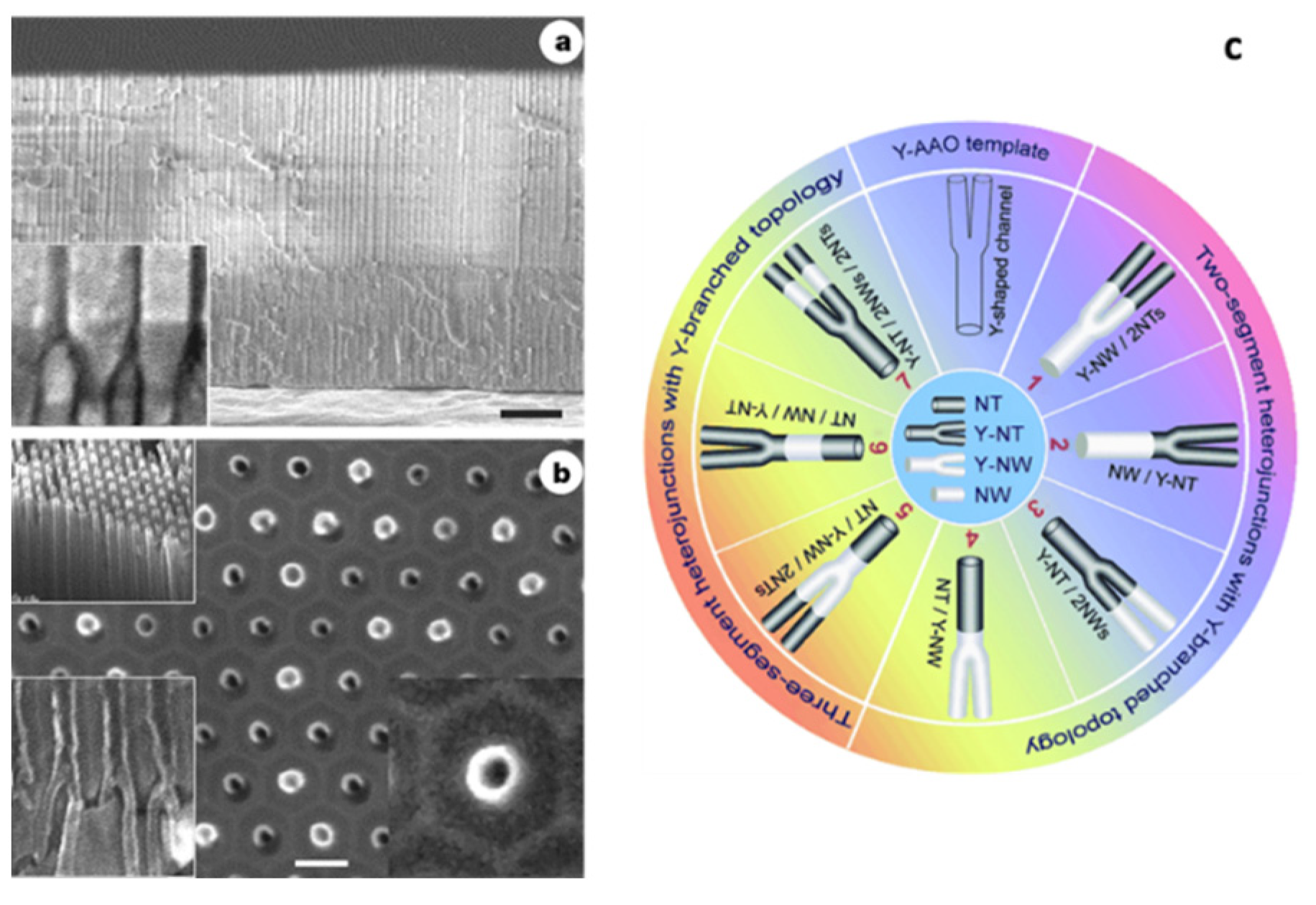
- Meng, G.; Han, F.; Zhao, X.; Chen, B.; Yang, D.; Liu, J.; Xu, Q.; Kong, M.; Zhu, X.; Jung, Y.J. A general synthetic approach to interconnected nanowire/nanotube and nanotube/nanowire/nanotube heterojunctions with branched topology. Angew. Chem. 2009, 121, 7302–7306. [Google Scholar] [CrossRef]
- Li, J.; Papadopoulos, C.; Xu, J. Growing Y-junction carbon nanotubes. Nature 1999, 402, 253–254. [Google Scholar] [CrossRef]
- Stępniowski, W.J.; Salerno, M. Fabrication of nanowires and nanotubes by anodic alumina template-assisted electrodeposition. Manuf. Nanostruct. 2014, 12, 321–357. [Google Scholar]
- Ke, N.J.; Downard, A.J.; Golovko, V.B. Carbon nanotube diameter control via catalytic Co nanoparticles electrodeposited in porous alumina membranes. RSC Adv. 2015, 5, 25747–25754. [Google Scholar] [CrossRef] [Green Version]
- Zhao, X.; Seo, S.-K.; Lee, U.-J.; Lee, K.-H. Controlled Electrochemical Dissolution of Anodic Aluminum Oxide for Preparation of Open-Through Pore Structures. J. Electrochem. Soc. 2007, 154, C553–C557. [Google Scholar] [CrossRef] [Green Version]
- Novoselov, K.S.; Jiang, D.; Schedin, F.; Booth, T.J.; Khotkevich, V.V.; Morozov, S.V.; Geim, A.K. Two-dimensional atomic crystals. Proc. Natl. Acad. Sci. USA 2005, 102, 10451–10453. [Google Scholar] [CrossRef] [Green Version]
- Zhan, H.; Garrett, D.J.; Apollo, N.V.; Ganesan, K.; Lau, D.; Prawer, S.; Cervenka, J. Direct fabrication of 3D graphene on nanoporous anodic alumina by plasma-enhanced chemical vapor deposition. Sci. Rep. 2016, 6, 19822. [Google Scholar] [CrossRef] [PubMed] [Green Version]
- Zhou, M.; Lin, T.; Huang, F.; Zhong, Y.; Wang, Z.; Tang, Y.; Bi, H.; Wan, D.; Lin, J. Highly Conductive Porous Graphene/Ceramic Composites for Heat Transfer and Thermal Energy Storage. Adv. Funct. Mater. 2013, 23, 2263–2269. [Google Scholar] [CrossRef]
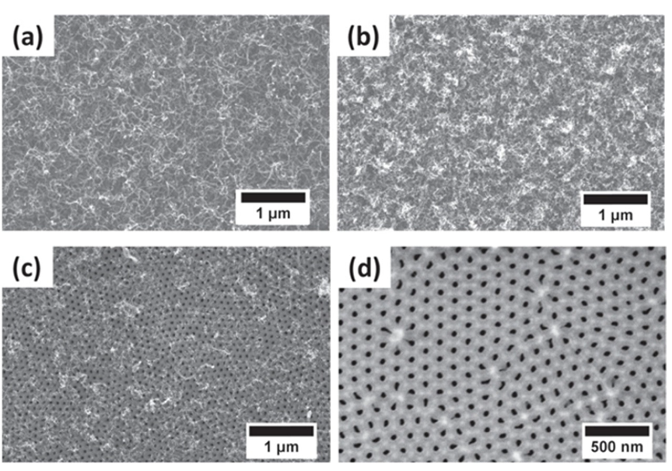
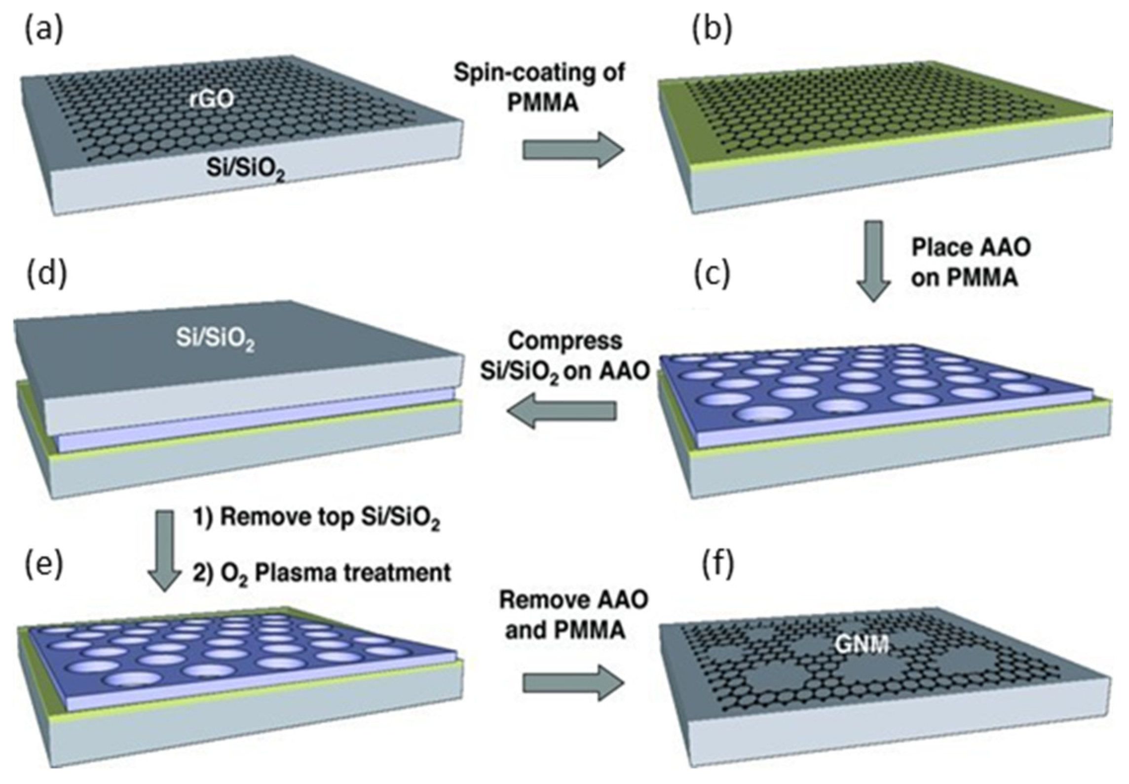
- Zeng, Z.; Huang, X.; Yin, Z.; Li, H.; Chen, Y.; Li, H.; Zhang, Q.; Ma, J.; Boey, F.; Zhang, H. Fabrication of Graphene Nanomesh by Using an Anodic Aluminum Oxide Membrane as a Template. Adv. Mater. 2012, 24, 4138–4142. [Google Scholar] [CrossRef] [PubMed]
- Lee, J.-H.; Jang, Y.; Heo, K.; Lee, J.-M.; Choi, S.H.; Joo, W.-J.; Hwang, S.W.; Whang, D. Large-scale fabrication of 2-D nanoporous graphene using a thin anodic aluminum oxide etching mask. J. Nanosci. Nanotechnol. 2013, 13, 7401–7405. [Google Scholar] [CrossRef]
- Kaur, G.; Kavitha, K.; Lahiri, I. Transfer-Free Graphene Growth on Dielectric Substrates: A Review of the Growth Mechanism. Crit. Rev. Solid State Mater. Sci. 2019, 44, 157–209. [Google Scholar] [CrossRef]
- Vollebregt, S.; Alfano, B.; Ricciardella, F.; Giesbers, A.J.M.; Grachova, Y.; Zeijl, H.W.v.; Polichetti, T.; Sarro, P.M. A transfer-free wafer-scale CVD graphene fabrication process for MEMS/NEMS sensors. In Proceedings of the 2016 IEEE 29th International Conference on Micro Electro Mechanical Systems (MEMS), Shanghai, China, 24–28 January 2016; pp. 17–20. [Google Scholar]
- Ricciardella, F.; Vollebregt, S.; Boshuizen, B.; Danzl, F.J.K.; Cesar, I.; Spinelli, P.; Sarro, P.M. Wafer-scale transfer-free process of multi-layered graphene grown by chemical vapor deposition. Mater. Res. Express 2020, 7, 35001. [Google Scholar] [CrossRef]
- Akhtar, S.; Ali, S.; Kafiah, F.M.; Ibrahim, A.; Matin, A.; Laoui, T. Preparation of graphene-coated anodic alumina substrates for selective molecular transport. Carbon Lett. 2020, 30, 23–33. [Google Scholar] [CrossRef]
- Zhang, Y.; Liu, Z.; Chen, A.; Wang, Q.; Zhang, J.; Zhao, C.; Xu, J.; Yang, W.; Peng, Y.; Zhang, Z. Fabrication of Micro-/Submicro-/Nanostructured Polypropylene/Graphene Superhydrophobic Surfaces with Extreme Dynamic Pressure Resistance Assisted by Single Hierarchically Porous Anodic Aluminum Oxide Template. J. Phys. Chem. C 2020, 124, 6197–6205. [Google Scholar] [CrossRef]
- Chen, W.; Gui, X.; Liang, B.; Yang, R.; Zheng, Y.; Zhao, C.; Li, X.; Zhu, H.; Tang, Z. Structural Engineering for High Sensitivity, Ultrathin Pressure Sensors Based on Wrinkled Graphene and Anodic Aluminum Oxide Membrane. ACS Appl. Mater. Interfaces 2017, 9, 24111–24117. [Google Scholar] [CrossRef]
- Petukhov, D.I.; Chernova, E.A.; Kapitanova, O.O.; Boytsova, O.V.; Valeev, R.G.; Chumakov, A.P.; Konovalov, O.V.; Eliseev, A.A. Thin graphene oxide membranes for gas dehumidification. J. Membr. Sci. 2019, 577, 184–194. [Google Scholar] [CrossRef]
- Tyagi, A.; Walia, R.S.; Murtaza, Q.; Pandey, S.M.; Tyagi, P.K.; Bajaj, B. A critical review of diamond like carbon coating for wear resistance applications. Int. J. Refract. Met. Hard Mater. 2019, 78, 107–122. [Google Scholar] [CrossRef]
- Liao, T.T.; Zhang, T.F.; Li, S.S.; Deng, Q.Y.; Wu, B.J.; Zhang, Y.Z.; Zhou, Y.J.; Guo, Y.B.; Leng, Y.X.; Huang, N. Biological responses of diamond-like carbon (DLC) films with different structures in biomedical application. Mater. Sci. Eng. C 2016, 69, 751–759. [Google Scholar] [CrossRef] [PubMed]
- Davoodi, E.; Zhianmanesh, M.; Montazerian, H.; Milani, A.S.; Hoorfar, M. Nano-porous anodic alumina: Fundamentals and applications in tissue engineering. J. Mater. Sci. Mater. Med. 2020, 31, 60. [Google Scholar] [CrossRef]
- Masuda, H.; Yanagishita, T.; Yasui, K.; Nishio, K.; Yagi, I.; Rao, T.N.; Fujishima, A. Synthesis of Well-Aligned Diamond Nanocylinders. Adv. Mater. 2001, 13, 247–249. [Google Scholar] [CrossRef]
- Yanagishita, T.; Nishio, K.; Nakao, M.; Fujishima, A.; Masuda, H. Synthesis of Diamond Cylinders with Triangular and Square Cross Sections Using Anodic Porous Alumina Templates. Chem. Lett. 2002, 31, 976–977. [Google Scholar] [CrossRef]
- Aramesh, M.; Fox, K.; Lau, D.W.M.; Fang, J.; Ostrikov, K.; Prawer, S.; Cervenka, J. Multifunctional three-dimensional nanodiamond-nanoporous alumina nanoarchitectures. Carbon 2014, 75, 452–464. [Google Scholar] [CrossRef]
- Alexander, M.R.; Beamson, G.; Bailey, P.; Noakes, T.C.Q.; Skeldon, P.; Thompson, G.E. The distribution of hydroxyl ions at the surface of anodic alumina. Surf. Interface Anal. 2003, 35, 649–657. [Google Scholar] [CrossRef]
- Aramesh, M.; Tong, W.; Fox, K.; Turnley, A.; Seo, D.H.; Prawer, S.; Ostrikov, K.K. Nanocarbon-coated porous anodic alumina for bionic devices. Materials 2015, 8, 4992–5006. [Google Scholar] [CrossRef] [Green Version]
- Karan, S.; Samitsu, S.; Peng, X.; Kurashima, K.; Ichinose, I. Ultrafast viscous permeation of organic solvents through diamond-like carbon nanosheets. Science 2012, 335, 444–447. [Google Scholar] [CrossRef]
- Tsai, H.-Y.; Tseng, P.-T. Field emission characteristics of diamond nano-tip array fabricated by anodic aluminum oxide template with nano-conical holes. Appl. Surf. Sci. 2015, 351, 1004–1010. [Google Scholar] [CrossRef]
- Zheng, J.; Lienhard, B.; Doerk, G.; Cotlet, M.; Bersin, E.; Kim, H.S.; Byun, Y.-C.; Nam, C.-Y.; Kim, J.; Black, C.T.; et al. Top-down fabrication of high-uniformity nanodiamonds by self-assembled block copolymer masks. Sci. Rep. 2019, 9, 6914. [Google Scholar] [CrossRef] [PubMed]
- Lin, C.-T.; Chen, W.-C.; Yen, M.-Y.; Wang, L.-S.; Lee, C.-Y.; Chin, T.-S.; Chiu, H.-T. Cone-stacked carbon nanofibers with cone angle increasing along the longitudinal axis. Carbon 2007, 45, 411–415. [Google Scholar] [CrossRef] [Green Version]
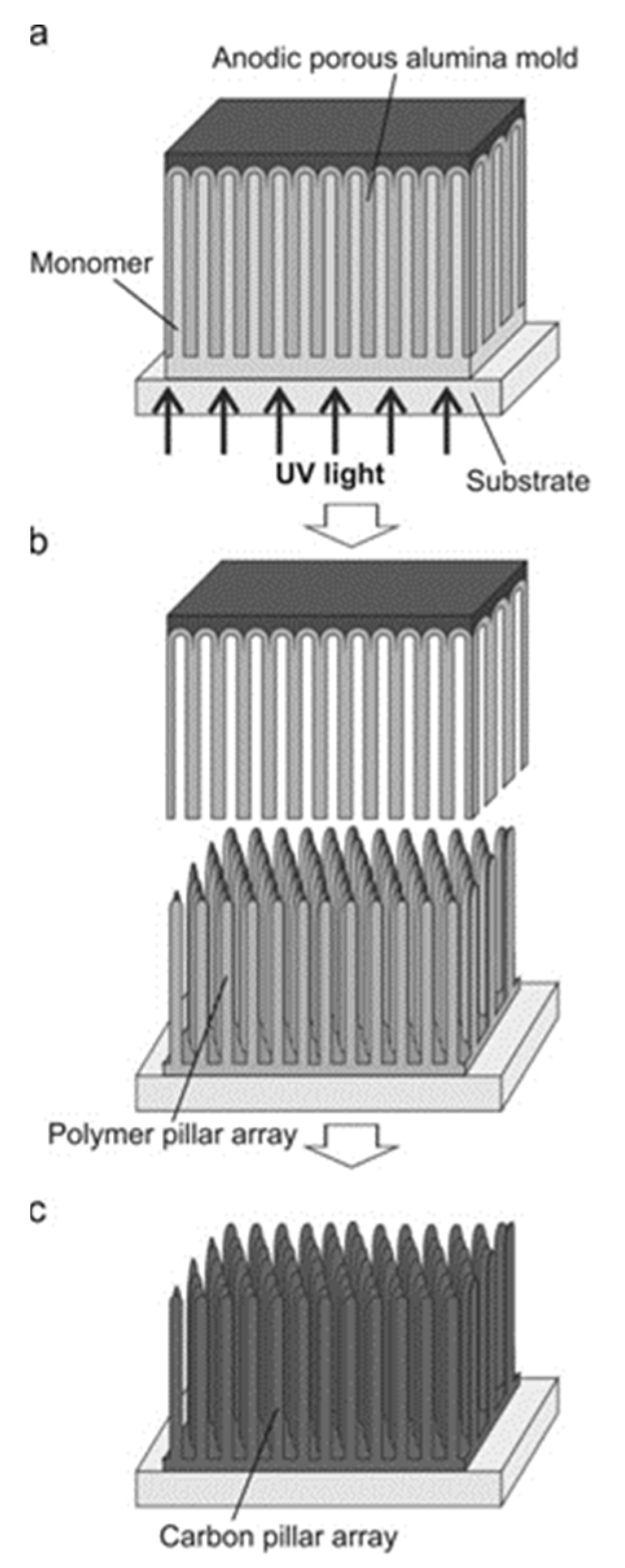
- Yanagishita, T.; Masuda, H. Carbon nanofiber arrays from high-aspect ratio polymer pillar prepared by nanoimprinting using anodic porous alumina. Mater. Lett. 2015, 160, 235–237. [Google Scholar] [CrossRef]
- Zhao, Y.; Chen, M.; Liu, W.; Liu, X.; Xue, Q. Preparation and self-lubrication treatment of ordered porous anodic alumina film. Mater. Chem. Phys. 2003, 82, 370–374. [Google Scholar] [CrossRef]
- Sui, Y.C.; Cui, B.Z.; Guardián, R.; Acosta, D.R.; Martínez, L.; Perez, R. Growth of carbon nanotubes and nanofibres in porous anodic alumina film. Carbon 2002, 40, 1011–1016. [Google Scholar] [CrossRef]
- Chun, H.; Hahm, M.G.; Homma, Y.; Meritz, R.; Kuramochi, K.; Menon, L.; Ci, L.; Ajayan, P.M.; Jung, Y.J. Engineering low-aspect ratio carbon nanostructures: Nanocups, nanorings, and nanocontainers. ACS Nano 2009, 3, 1274–1278. [Google Scholar] [CrossRef]
- Matthews, M.J.; Pimenta, M.A.; Dresselhaus, G.; Dresselhaus, M.S.; Endo, M. Origin of dispersive effects of the Raman D band in carbon materials. Phys. Rev. B 1999, 59, R6585–R6588. [Google Scholar] [CrossRef]
- Habazaki, H.; Kiriu, M.; Konno, H. High rate capability of carbon nanofilaments with platelet structure as anode materials for lithium ion batteries. Electrochem. Commun. 2006, 8, 1275–1279. [Google Scholar] [CrossRef] [Green Version]
- Habazaki, H.; Kiriu, M.; Hayashi, M.; Konno, H. Structure of the carbon nanofilaments formed by liquid phase carbonization in porous anodic alumina template. Mater. Chem. Phys. 2007, 105, 367–372. [Google Scholar] [CrossRef] [Green Version]
- Tsuji, E.; Yamasaki, T.; Aoki, Y.; Park, S.-G.; Shimizu, K.-i.; Habazaki, H. Highly durable platelet carbon nanofiber-supported platinum catalysts for the oxygen reduction reaction. Carbon 2015, 87, 1–9. [Google Scholar] [CrossRef]
- Sato, Y.; Kowalski, D.; Aoki, Y.; Habazaki, H. Long-term durability of platelet-type carbon nanofibers for OER and ORR in highly alkaline media. Appl. Catal. A Gen. 2020, 597, 117555. [Google Scholar] [CrossRef]
- Lin, C.-T.; Chen, T.-H.; Chin, T.-S.; Lee, C.-Y.; Chiu, H.-T. Quasi two-dimensional carbon nanobelts synthesized using a template method. Carbon 2008, 46, 741–746. [Google Scholar] [CrossRef]
- Xu, L.; Li, S.; Wu, Z.; Li, H.; Yan, D.; Zhang, C.; Zhang, P.; Yan, P.; Li, X. Growth and field emission properties of nanotip arrays of amorphous carbon with embedded hexagonal diamond nanoparticles. Appl. Phys. A 2011, 103, 59–65. [Google Scholar] [CrossRef]
- Zhang, P.J.; Chen, J.T.; Zhuo, R.F.; Xu, L.; Lu, Q.H.; Ji, X.; Yan, P.X.; Wu, Z.G. Carbon nanodot arrays grown as replicas of specially widened anodic aluminum oxide pore arrays. Appl. Surf. Sci. 2009, 255, 4456–4460. [Google Scholar] [CrossRef]
- Wu, Z.; Li, W.; Xu, L.; Li, S.; Zhang, C.; Yan, P. The preparation of Al-containing amorphous carbon nanotip arrays and their excellent field emission properties. Appl. Surf. Sci. 2012, 258, 7918–7921. [Google Scholar] [CrossRef]
- Fan, D.H.; Ding, G.Q.; Shen, W.Z.; Zheng, M.J. Anion impurities in porous alumina membranes: Existence and functionality. Microporous Mesoporous Mater. 2007, 100, 154–159. [Google Scholar] [CrossRef]
- Kumeria, T.; Santos, A.; Losic, D. Nanoporous Anodic Alumina Platforms: Engineered Surface Chemistry and Structure for Optical Sensing Applications. Sensors 2014, 14, 11878–11918. [Google Scholar] [CrossRef] [Green Version]
- Alekseev, N.I.; Filippov, B.M.; Basargin, I.V.; Sedov, A.I. Investigation of semicommercial arc plants for fullerene-production. J. Eng. Phys. Thermophys. 2011, 84, 1087–1098. [Google Scholar] [CrossRef]
- Mojica, M.; Alonso, J.A.; Méndez, F. Synthesis of fullerenes. J. Phys. Org. Chem. 2013, 26, 526–539. [Google Scholar] [CrossRef]
- Tao, F.; Liang, Y.; Yin, G.; Xu, D.; Jiang, Z.; Li, H.; Han, M.; Song, Y.; Xie, Z.; Xue, Z.; et al. Concentric Sub-micrometer-Sized Cables Composed of Ni Nanowires and Sub-micrometer-Sized Fullerene Tubes. Adv. Funct. Mater. 2007, 17, 1124–1130. [Google Scholar] [CrossRef]
- Guo, Y.G.; Li, C.J.; Wan, L.J.; Chen, D.M.; Wang, C.R.; Bai, C.L.; Wang, Y.G. Well-Defined Fullerene Nanowire Arrays. Adv. Funct. Mater. 2003, 13, 626–630. [Google Scholar] [CrossRef]
- Ringor, C.L.; Miyazawa, K. Synthesis of C60 nanotubes by liquid–liquid interfacial precipitation method: Influence of solvent ratio, growth temperature, and light illumination. Diam. Relat. Mater. 2008, 17, 529–534. [Google Scholar] [CrossRef]
- Miyazawa, K.i.; Kuriyama, R.; Shimomura, S.; Wakahara, T.; Tachibana, M. Growth and FIB-SEM analyses of C60 microtubes vertically synthesized on porous alumina membranes. J. Cryst. Growth 2014, 388, 5–11. [Google Scholar] [CrossRef]
- Zhao, H.; Zhou, M.; Wen, L.; Lei, Y. Template-directed construction of nanostructure arrays for highly-efficient energy storage and conversion. Nano Energy 2015, 13, 790–813. [Google Scholar] [CrossRef]
- Niu, T. Carbon nanotubes advance next-generation electronics. Nano Today 2020, 35, 100992. [Google Scholar] [CrossRef]
- Choi, W.B.; Chu, J.U.; Jeong, K.S.; Bae, E.J.; Lee, J.-W.; Kim, J.-J.; Lee, J.-O. Ultrahigh-density nanotransistors by using selectively grown vertical carbon nanotubes. Appl. Phys. Lett. 2001, 79, 3696–3698. [Google Scholar] [CrossRef]
- Franklin, A.D.; Sayer, R.A.; Sands, T.D.; Janes, D.B.; Fisher, T.S. Vertical Carbon Nanotube Devices With Nanoscale Lengths Controlled Without Lithography. IEEE Trans. Nanotechnol. 2009, 8, 469–476. [Google Scholar] [CrossRef] [Green Version]
- Collins, P.G.; Arnold, M.S.; Avouris, P. Engineering carbon nanotubes and nanotube circuits using electrical breakdown. Science 2001, 292, 706–709. [Google Scholar] [CrossRef]
- Kim, H.; Gao, S.; Hahm, M.G.; Ahn, C.W.; Jung, H.Y.; Jung, Y.J. Graphitic Nanocup Architectures for Advanced Nanotechnology Applications. Nanomaterials 2020, 10, 1862. [Google Scholar] [CrossRef]
- Jung, H.Y.; Karimi, M.B.; Hahm, M.G.; Ajayan, P.M.; Jung, Y.J. Transparent, flexible supercapacitors from nano-engineered carbon films. Sci. Rep. 2012, 2, 773. [Google Scholar] [CrossRef] [Green Version]
- Hahm, M.G.; Leela Mohana Reddy, A.; Cole, D.P.; Rivera, M.; Vento, J.A.; Nam, J.; Jung, H.Y.; Kim, Y.L.; Narayanan, N.T.; Hashim, D.P.; et al. Carbon Nanotube–Nanocup Hybrid Structures for High Power Supercapacitor Applications. Nano Lett. 2012, 12, 5616–5621. [Google Scholar] [CrossRef] [PubMed]
- Jung, H.Y.; Chun, H.; Park, S.; Kang, S.-H.; Ahn, C.W.; Kwon, Y.-K.; Upmanyu, M.; Ajayan, P.M.; Jung, Y.J. Liquid metal nanodroplet dynamics inside nanocontainers. Sci. Rep. 2013, 3, 2588. [Google Scholar] [CrossRef] [PubMed] [Green Version]
- Palneedi, H.; Peddigari, M.; Hwang, G.-T.; Jeong, D.-Y.; Ryu, J. High-Performance Dielectric Ceramic Films for Energy Storage Capacitors: Progress and Outlook. Adv. Funct. Mater. 2018, 28, 1803665. [Google Scholar] [CrossRef]
- Han, F.; Meng, G.; Zhou, F.; Song, L.; Li, X.; Hu, X.; Zhu, X.; Wu, B.; Wei, B. Dielectric capacitors with three-dimensional nanoscale interdigital electrodes for energy storage. Sci. Adv. 2015, 1, e1500605. [Google Scholar] [CrossRef] [PubMed] [Green Version]
- Hu, J.; Zhang, S.; Tang, B. Rational design of nanomaterials for high energy density dielectric capacitors via electrospinning. Energy Storage Mater. 2021, 37, 530–555. [Google Scholar] [CrossRef]
- Zheng, G.; Yang, Y.; Cha, J.J.; Hong, S.S.; Cui, Y. Hollow Carbon Nanofiber-Encapsulated Sulfur Cathodes for High Specific Capacity Rechargeable Lithium Batteries. Nano Lett. 2011, 11, 4462–4467. [Google Scholar] [CrossRef]
- Chung, S.-H.; Manthiram, A. Current Status and Future Prospects of Metal–Sulfur Batteries. Adv. Mater. 2019, 31, 1901125. [Google Scholar] [CrossRef]
- Zheng, G.; Zhang, Q.; Cha, J.J.; Yang, Y.; Li, W.; Seh, Z.W.; Cui, Y. Amphiphilic Surface Modification of Hollow Carbon Nanofibers for Improved Cycle Life of Lithium Sulfur Batteries. Nano Lett. 2013, 13, 1265–1270. [Google Scholar] [CrossRef]
- Gibot, P.; Casas-Cabanas, M.; Laffont, L.; Levasseur, S.; Carlach, P.; Hamelet, S.; Tarascon, J.-M.; Masquelier, C. Room-temperature single-phase Li insertion/extraction in nanoscale LixFePO4. Nat. Mater. 2008, 7, 741–747. [Google Scholar] [CrossRef]
- Peng, X.-X.; Lu, Y.-Q.; Zhou, L.-L.; Sheng, T.; Shen, S.-Y.; Liao, H.-G.; Huang, L.; Li, J.-T.; Sun, S.-G. Graphitized porous carbon materials with high sulfur loading for lithium-sulfur batteries. Nano Energy 2017, 32, 503–510. [Google Scholar] [CrossRef]
- Liu, Y.; Elias, Y.; Meng, J.; Aurbach, D.; Zou, R.; Xia, D.; Pang, Q. Electrolyte solutions design for lithium-sulfur batteries. Joule 2021, 5, 2323–2364. [Google Scholar] [CrossRef]
- Cheng, Y.; Jiang, S.P. Advances in electrocatalysts for oxygen evolution reaction of water electrolysis-from metal oxides to carbon nanotubes. Prog. Nat. Sci. Mater. Int. 2015, 25, 545–553. [Google Scholar] [CrossRef] [Green Version]
- Mohideen, M.M.; Liu, Y.; Ramakrishna, S. Recent progress of carbon dots and carbon nanotubes applied in oxygen reduction reaction of fuel cell for transportation. Appl. Energy 2020, 257, 114027. [Google Scholar] [CrossRef]
- Zhao, X.; Li, F.; Wang, R.; Seo, J.-M.; Choi, H.-J.; Jung, S.-M.; Mahmood, J.; Jeon, I.-Y.; Baek, J.-B. Controlled Fabrication of Hierarchically Structured Nitrogen-Doped Carbon Nanotubes as a Highly Active Bifunctional Oxygen Electrocatalyst. Adv. Funct. Mater. 2017, 27, 1605717. [Google Scholar] [CrossRef]
- Liang, Y.; Wang, H.; Diao, P.; Chang, W.; Hong, G.; Li, Y.; Gong, M.; Xie, L.; Zhou, J.; Wang, J.; et al. Oxygen Reduction Electrocatalyst Based on Strongly Coupled Cobalt Oxide Nanocrystals and Carbon Nanotubes. J. Am. Chem. Soc. 2012, 134, 15849–15857. [Google Scholar] [CrossRef]
- Tao, L.; Wang, Q.; Dou, S.; Ma, Z.; Huo, J.; Wang, S.; Dai, L. Edge-rich and dopant-free graphene as a highly efficient metal-free electrocatalyst for the oxygen reduction reaction. Chem. Commun. 2016, 52, 2764–2767. [Google Scholar] [CrossRef]
- Altalhi, T.; Kumeria, T.; Santos, A.; Losic, D. Synthesis of well-organised carbon nanotube membranes from non-degradable plastic bags with tuneable molecular transport: Towards nanotechnological recycling. Carbon 2013, 63, 423–433. [Google Scholar] [CrossRef]
- Altalhi, T.; Ginic-Markovic, M.; Han, N.; Clarke, S.; Losic, D. Synthesis of carbon nanotube (CNT) composite membranes. Membranes 2011, 1, 37–47. [Google Scholar] [CrossRef] [Green Version]
- Mattia, D.; Leese, H.; Lee, K.P. Carbon nanotube membranes: From flow enhancement to permeability. J. Membr. Sci. 2015, 475, 266–272. [Google Scholar] [CrossRef] [Green Version]
- Rana, K.; Kucukayan-Dogu, G.; Bengu, E. Growth of vertically aligned carbon nanotubes over self-ordered nano-porous alumina films and their surface properties. Appl. Surf. Sci. 2012, 258, 7112–7117. [Google Scholar] [CrossRef]
- Jafari, A.; Mahvi, A.H.; Nasseri, S.; Rashidi, A.; Nabizadeh, R.; Rezaee, R. Ultrafiltration of natural organic matter from water by vertically aligned carbon nanotube membrane. J. Environ. Health Sci. Eng. 2015, 13, 51. [Google Scholar] [CrossRef] [PubMed]
- Zhang, R.; Zhang, Y.; Wei, F. Horizontally aligned carbon nanotube arrays: Growth mechanism, controlled synthesis, characterization, properties and applications. Chem. Soc. Rev. 2017, 46, 3661–3715. [Google Scholar] [CrossRef]
- He, M.; Zhang, S.; Zhang, J. Horizontal Single-Walled Carbon Nanotube Arrays: Controlled Synthesis, Characterizations, and Applications. Chem. Rev. 2020, 120, 12592–12684. [Google Scholar] [CrossRef]
- Hoa, N.D.; Van Quy, N.; Cho, Y.; Kim, D. An ammonia gas sensor based on non-catalytically synthesized carbon nanotubes on an anodic aluminum oxide template. Sens. Actuators B Chem. 2007, 127, 447–454. [Google Scholar] [CrossRef]
- Ding, D.; Chen, Z.; Rajaputra, S.; Singh, V. Hydrogen sensors based on aligned carbon nanotubes in an anodic aluminum oxide template with palladium as a top electrode. Sens. Actuators B Chem. 2007, 124, 12–17. [Google Scholar] [CrossRef]
- Rajaputra, S.; Mangu, R.; Clore, P.; Qian, D.; Andrews, R.; Singh, V.P. Multi-walled carbon nanotube arrays for gas sensing applications. Nanotechnology 2008, 19, 345502. [Google Scholar] [CrossRef]
- Mangu, R.; Rajaputra, S.; Clore, P.; Qian, D.; Andrews, R.; Singh, V.P. Ammonia sensing properties of multiwalled carbon nanotubes embedded in porous alumina templates. Mater. Sci. Eng. B 2010, 174, 2–8. [Google Scholar] [CrossRef]
- Dhall, S.; Jaggi, N.; Nathawat, R. Functionalized multiwalled carbon nanotubes based hydrogen gas sensor. Sens. Actuators A Phys. 2013, 201, 321–327. [Google Scholar] [CrossRef]
- Tang, H.; Li, Y.; Sokolovskij, R.; Sacco, L.; Zheng, H.; Ye, H.; Yu, H.; Fan, X.; Tian, H.; Ren, T.L.; et al. Ultra-High Sensitive NO2 Gas Sensor Based on Tunable Polarity Transport in CVD-WS2/IGZO p-N Heterojunction. ACS Appl. Mater. Interfaces 2019, 11, 40850–40859. [Google Scholar] [CrossRef]
- Chen, Y.; Meng, F.; Li, M.; Liu, J. Novel capacitive sensor: Fabrication from carbon nanotube arrays and sensing property characterization. Sens. Actuators B Chem. 2009, 140, 396–401. [Google Scholar] [CrossRef]
- Tang, H.; Sacco, L.N.; Vollebregt, S.; Ye, H.; Fan, X.; Zhang, G. Recent advances in 2D/nanostructured metal sulfides-based gas sensors: Mechanisms, applications, and perspectives. J. Mater. Chem. A 2020, 8, 24943–24976. [Google Scholar] [CrossRef]
- Kwak, D.; Lei, Y.; Maric, R. Ammonia gas sensors: A comprehensive review. Talanta 2019, 204, 713–730. [Google Scholar] [CrossRef] [PubMed]
- Penza, M.; Rossi, R.; Alvisi, M.; Serra, E. Metal-modified and vertically aligned carbon nanotube sensors array for landfill gas monitoring applications. Nanotechnology 2010, 21, 105501. [Google Scholar] [CrossRef] [PubMed] [Green Version]
- Tian, Y.; Zhang, L.; Wang, L. DNA-Functionalized Plasmonic Nanomaterials for Optical Biosensing. Biotechnol. J. 2020, 15, e1800741. [Google Scholar] [CrossRef] [PubMed]
- Purohit, B.; Vernekar, P.R.; Shetti, N.P.; Chandra, P. Biosensor nanoengineering: Design, operation, and implementation for biomolecular analysis. Sens. Int. 2020, 1, 100040. [Google Scholar] [CrossRef]
- Claussen, J.C.; Franklin, A.D.; ul Haque, A.; Porterfield, D.M.; Fisher, T.S. Electrochemical Biosensor of Nanocube-Augmented Carbon Nanotube Networks. ACS Nano 2009, 3, 37–44. [Google Scholar] [CrossRef]
- Claussen, J.C.; Artiles, M.S.; McLamore, E.S.; Mohanty, S.; Shi, J.; Rickus, J.L.; Fisher, T.S.; Porterfield, D.M. Electrochemical glutamate biosensing with nanocube and nanosphere augmented single-walled carbon nanotube networks: A comparative study. J. Mater. Chem. 2011, 21, 11224–11231. [Google Scholar] [CrossRef]
- Zhou, Y.; Danbolt, N.C. Glutamate as a neurotransmitter in the healthy brain. J. Neural Transm. 2014, 121, 799–817. [Google Scholar] [CrossRef] [Green Version]
- Schultz, J.; Uddin, Z.; Singh, G.; Howlader, M.M.R. Glutamate sensing in biofluids: Recent advances and research challenges of electrochemical sensors. Analyst 2020, 145, 321–347. [Google Scholar] [CrossRef]
- Qiao, Z.; Zhang, H.; Zhou, Y.; Zheng, J. C60 Mediated Ion Pair Interaction for Label-Free Electrochemical Immunosensing with Nanoporous Anodic Alumina Nanochannels. Anal. Chem. 2019, 91, 5125–5132. [Google Scholar] [CrossRef]
- Rajeev, G.; Prieto Simon, B.; Marsal, L.F.; Voelcker, N.H. Advances in Nanoporous Anodic Alumina-Based Biosensors to Detect Biomarkers of Clinical Significance: A Review. Adv. Healthc. Mater. 2018, 7, 1700904. [Google Scholar] [CrossRef] [PubMed]
- Han, J.; Zhuo, Y.; Chai, Y.-Q.; Xiang, Y.; Yuan, R. New Type of Redox Nanoprobe: C60-Based Nanomaterial and Its Application in Electrochemical Immunoassay for Doping Detection. Anal. Chem. 2015, 87, 1669–1675. [Google Scholar] [CrossRef]
- Yu, J.; Luo, P.; Xin, C.; Cao, X.; Zhang, Y.; Liu, S. Quantitative Evaluation of Biological Reaction Kinetics in Confined Nanospaces. Anal. Chem. 2014, 86, 8129–8135. [Google Scholar] [CrossRef] [PubMed]
- Kim, J.; Liu, Q.; Cui, T. Graphene-Based Ion Sensitive-FET Sensor With Porous Anodic Aluminum Oxide Substrate for Nitrate Detection. J. Microelectromech. Syst. 2020, 29, 966–971. [Google Scholar] [CrossRef]
- Jackson, D.T.; Nelson, P.N. Preparation and properties of some ion selective membranes: A review. J. Mol. Struct. 2019, 1182, 241–259. [Google Scholar] [CrossRef]
- Daniel, W.L.; Han, M.S.; Lee, J.-S.; Mirkin, C.A. Colorimetric Nitrite and Nitrate Detection with Gold Nanoparticle Probes and Kinetic End Points. J. Am. Chem. Soc. 2009, 131, 6362–6363. [Google Scholar] [CrossRef]
- He, J.; Xiao, P.; Lu, W.; Shi, J.; Zhang, L.; Liang, Y.; Pan, C.; Kuo, S.-W.; Chen, T. A Universal high accuracy wearable pulse monitoring system via high sensitivity and large linearity graphene pressure sensor. Nano Energy 2019, 59, 422–433. [Google Scholar] [CrossRef]
- Chen, K.-Y.; Xu, Y.-T.; Zhao, Y.; Li, J.-K.; Wang, X.-P.; Qu, L.-T. Recent progress in graphene-based wearable piezoresistive sensors: From 1D to 3D device geometries. Nano Mater. Sci. 2022; in press. [Google Scholar] [CrossRef]
- Santos, J.S.; Araújo, P.d.S.; Pissolitto, Y.B.; Lopes, P.P.; Simon, A.P.; Sikora, M.d.S.; Trivinho-Strixino, F. The Use of Anodic Oxides in Practical and Sustainable Devices for Energy Conversion and Storage. Materials 2021, 14, 383. [Google Scholar] [CrossRef] [PubMed]
- Kothari, A.K.; Konca, E.; Sheldon, B.W.; Jian, K.; Li, H.; Xia, Z.; Ni, W.; Hurt, R. Mechanical behavior of anodic alumina coatings reinforced with carbon nanofibers. J. Mater. Sci. 2009, 44, 6020–6027. [Google Scholar] [CrossRef]
- Aramesh, M.; Cervenka, J. Surface modification of porous anodic alumina for medical and biological applications. Nanomedicine 2014, 438, 438. [Google Scholar]
- Fischer, N.; Claeys, M. In situ characterization of Fischer–Tropsch catalysts: A review. J. Phys. D Appl. Phys. 2020, 53, 293001. [Google Scholar] [CrossRef]
- Martín, J.; Martín-González, M.; Francisco Fernández, J.; Caballero-Calero, O. Ordered three-dimensional interconnected nanoarchitectures in anodic porous alumina. Nat. Commun. 2014, 5, 5130. [Google Scholar] [CrossRef] [PubMed] [Green Version]
- Meier, L.A.; Alvarez, A.E.; Salinas, D.R.; del Barrio, M.C. A clean method to obtain a porous alumina template. Mater. Lett. 2012, 70, 119–121. [Google Scholar] [CrossRef]
- Zhang, H.; Zhou, M.; Zhao, H.; Lei, Y. Ordered nanostructures arrays fabricated by anodic aluminum oxide (AAO) template-directed methods for energy conversion. Nanotechnology 2021, 32, 502006. [Google Scholar] [CrossRef] [PubMed]
- Makgabutlane, B.; Nthunya, L.N.; Maubane-Nkadimeng, M.S.; Mhlanga, S.D. Green synthesis of carbon nanotubes to address the water-energy-food nexus: A critical review. J. Environ. Chem. Eng. 2021, 9, 104736. [Google Scholar] [CrossRef]
- Bakierska, M.; Lis, M.; Pacek, J.; Świętosławski, M.; Gajewska, M.; Tąta, A.; Proniewicz, E.; Molenda, M. Bio-derived carbon nanostructures for high-performance lithium-ion batteries. Carbon 2019, 145, 426–432. [Google Scholar] [CrossRef]
- Gao, Z.; Zhao, M.-Q.; Alam Ashik, M.M.; Johnson, A.T.C. Recentadvances in the propertiesand synthesis of bilayer graphene and transition metal dichalcogenides. J. Phys. Mater. 2020, 3, 42003. [Google Scholar] [CrossRef]
- Gross, S.; Vittadini, A.; Dengo, N. Functionalisation of Colloidal Transition Metal Sulphides Nanocrystals: A Fascinating and Challenging Playground for the Chemist. Crystals 2017, 7, 110. [Google Scholar] [CrossRef] [Green Version]
- Valeev, R.; Romanov, E.; Beltukov, A.; Mukhgalin, V.; Roslyakov, I.; Eliseev, A. Structure and luminescence characteristics of ZnS nanodot array in porous anodic aluminum oxide. Phys. Status Solidi C 2012, 9, 1462–1465. [Google Scholar] [CrossRef]
- Valeev, R.G.; Trigub, A.L.; Beltiukov, A.N.; Petukhov, D.I.; El’kin, I.A.; Stashkova, V.V. Nanostructured ZnS: Cu(Mn) Coatings on the Surface of Porous Anodic Alumina for Optical Applications. J. Surf. Investig. X-Ray Synchrotron Neutron Tech. 2019, 13, 92–100. [Google Scholar] [CrossRef]
- Demchyshyn, S.; Roemer, J.M.; Groiß, H.; Heilbrunner, H.; Ulbricht, C.; Apaydin, D.; Böhm, A.; Rütt, U.; Bertram, F.; Hesser, G.; et al. Confining metal-halide perovskites in nanoporous thin films. Sci. Adv. 2017, 3, e1700738. [Google Scholar] [CrossRef] [PubMed]
- Liu, C.; Hong, H.; Wang, Q.; Liu, P.; Zuo, Y.; Liang, J.; Cheng, Y.; Zhou, X.; Wang, J.; Zhao, Y. Strong-coupled hybrid structure of carbon nanotube and MoS 2 monolayer with ultrafast interfacial charge transfer. Nanoscale 2019, 11, 17195–17200. [Google Scholar] [CrossRef] [PubMed]
- Luo, Q.; Wu, R.; Ma, L.; Wang, C.; Liu, H.; Lin, H.; Wang, N.; Chen, Y.; Guo, Z. Recent Advances on Carbon Nanotube Utilizations in Perovskite Solar Cells. Adv. Funct. Mater. 2020, 31, 2004765. [Google Scholar] [CrossRef]
- Pomerantseva, E.; Bonaccorso, F.; Feng, X.; Cui, Y.; Gogotsi, Y. Energy storage: The future enabled by nanomaterials. Science 2019, 366, eaan8285. [Google Scholar] [CrossRef] [Green Version]
- Wei, Q.; Fu, Y.; Zhang, G.; Yang, D.; Meng, G.; Sun, S. Rational design of novel nanostructured arrays based on porous AAO templates for electrochemical energy storage and conversion. Nano Energy 2019, 55, 234–259. [Google Scholar] [CrossRef]
- Dong, Y.; Xie, Y.; Xu, C.; Fu, Y.; Fan, X.; Li, X.; Wang, L.; Xiong, F.; Guo, W.; Pan, G.; et al. Transfer-free, lithography-free and fast growth of patterned CVD graphene directly on insulators by using sacrificial metal catalyst. Nanotechnology 2018, 29, 365301. [Google Scholar] [CrossRef]
- Vasiliev, A.A.; Pisliakov, A.V.; Sokolov, A.V.; Samotaev, N.N.; Soloviev, S.A.; Oblov, K.; Guarnieri, V.; Lorenzelli, L.; Brunelli, J.; Maglione, A.; et al. Non-silicon MEMS platforms for gas sensors. Sens. Actuators B Chem. 2016, 224, 700–713. [Google Scholar] [CrossRef]
- Srivastava, A.K.; Dwivedi, N.; Dhand, C.; Khan, R.; Sathish, N.; Gupta, M.K.; Kumar, R.; Kumar, S. Potential of graphene-based materials to combat COVID-19: Properties, perspectives, and prospects. Mater. Today Chem. 2020, 18, 100385. [Google Scholar] [CrossRef]
- Welch, E.C.; Powell, J.M.; Clevinger, T.B.; Fairman, A.E.; Shukla, A. Advances in Biosensors and Diagnostic Technologies Using Nanostructures and Nanomaterials. Adv. Funct. Mater. 2021, 31, 2104126. [Google Scholar] [CrossRef]
- Ye, W.; Zhang, Y.; Hu, W.; Wang, L.; Wang, P. A Sensitive FRET Biosensor Based on Carbon Dots-Modified Nanoporous Membrane for 8-hydroxy-2′-Deoxyguanosine (8-OHdG) Detection with Au@ ZIF-8 Nanoparticles as Signal Quenchers. Nanomaterials 2020, 10, 2044. [Google Scholar] [CrossRef] [PubMed]
- Guo, Y.; Gao, S.; Yue, W.; Zhang, C.; Li, Y. Anodized Aluminum Oxide-Assisted Low-Cost Flexible Capacitive Pressure Sensors Based on Double-Sided Nanopillars by a Facile Fabrication Method. ACS Appl. Mater. Interfaces 2019, 11, 48594–48603. [Google Scholar] [CrossRef] [PubMed]
- Drozdova, M.; Hussainova, I.; Pérez-Coll, D.; Aghayan, M.; Ivanov, R.; Rodríguez, M.A. A novel approach to electroconductive ceramics filled by graphene covered nanofibers. Mater. Des. 2016, 90, 291–298. [Google Scholar] [CrossRef]


| Application | Strength | Weakness | Perspective/Opportunity |
|---|---|---|---|
| Electronic devices | PAA can offer a collective organization and individual electronic units in each nanopore. The dielectric properties of the alumina can be useful to use as an insulator layer. | The synthesis of semi-conductive carbon nanomaterials is very complicated to precisely control. | Few publications were devoted to these kinds of devices the recent years. Transfer-free graphene nanoribbons or graphene nanodots as proposed in this review can revitalize the electronic applications based on PAA/graphene-based assemblies. |
| Energy conversion and storage devices | The PAA easily tailored structure and the facility to functionalize the carbon nanostructures leads to already efficient energy storage devices without the utilization of precious metals, generally used as electrodes. | Much progress has been achieved in laboratory research but no commercial products were reported. | More complex PAA nano-architectures needs to be explored to improve the energy storage and conversion technologies [315]. |
| Molecular Transport | The structural and geometrical features are easy to control on the development of a template-assisted catalyst-free CVD approach. | Catalytic synthesis of carbon excludes in this kind of application since the PAA needs to be open from both sides [267]. | A graphene transfer-free process can be interesting to fabricate PAA/graphene membranes avoiding the defects that can induce the transferring process, such as wrinkles, holes or contaminants [316]. |
| Photonic devices | Carbon nanostructures can be easily functionalized by the electrodeposition process. | To expose the carbon materials to the environment Lateral-PAA are required and carbon nanostructures emerge from the pores. This horizontal geometry is much complex to precisely control. | Fabrication of 3D-PAA architectures can be interesting to increase the exposure of carbon nanostructures within the host PAA matrix [302]. |
| Gas sensors | Easy implementation and cost-competitive price make PAA/Carbon-based gas sensors an attractive platform to develop the applications. | The electrode configuration is crucial for the interaction between the carbon nanostructure and the gas molecule. Also, in a chemiresitor configuration, the PAA walls can absorb gas analytes decreasing the sensor sensitivity and gas desorption. | The chemical stability of PAA/Carbon nanostructures can be attractive to operate under harsh environments [317]. |
| Biosensing and electrochemical sensing | PAA membrane and graphitic structures both have an extensive surface area that creates additional binding sites to immobilize bioreceptor molecules [318]. | Bridging between research lab to real-life applications is still an issue [319]. | Further functionalization of PAA/Carbon-based structures can be useful to expand the optical measurement of biomarkers [320]. |
| Pressure sensor | High optical transmittance of PAA and graphene are interesting to develop transparent sensors. | CNTs growth inside PAA templates can be difficultly implemented to develop this kind of application. | Flexible pressure sensors can be explored [321]. |
| Composite materials | The PAA coated carbon can increase the mechanical and tribological characteristics [155]. | The catalyst-free template approach used to fabricate PAA/Carbon-based composites leads to carbon nanostructures with more crystal lattice defects. | Electroconductive alumina can be an easily up-scalable method [322]. The bio-compatibility needs to be further studied. |
Disclaimer/Publisher’s Note: The statements, opinions and data contained in all publications are solely those of the individual author(s) and contributor(s) and not of MDPI and/or the editor(s). MDPI and/or the editor(s) disclaim responsibility for any injury to people or property resulting from any ideas, methods, instructions or products referred to in the content. |
© 2023 by the authors. Licensee MDPI, Basel, Switzerland. This article is an open access article distributed under the terms and conditions of the Creative Commons Attribution (CC BY) license (https://creativecommons.org/licenses/by/4.0/).
Share and Cite
Sacco, L.N.; Vollebregt, S. Overview of Engineering Carbon Nanomaterials Such As Carbon Nanotubes (CNTs), Carbon Nanofibers (CNFs), Graphene and Nanodiamonds and Other Carbon Allotropes inside Porous Anodic Alumina (PAA) Templates. Nanomaterials 2023, 13, 260. https://0-doi-org.brum.beds.ac.uk/10.3390/nano13020260
Sacco LN, Vollebregt S. Overview of Engineering Carbon Nanomaterials Such As Carbon Nanotubes (CNTs), Carbon Nanofibers (CNFs), Graphene and Nanodiamonds and Other Carbon Allotropes inside Porous Anodic Alumina (PAA) Templates. Nanomaterials. 2023; 13(2):260. https://0-doi-org.brum.beds.ac.uk/10.3390/nano13020260
Chicago/Turabian StyleSacco, Leandro Nicolás, and Sten Vollebregt. 2023. "Overview of Engineering Carbon Nanomaterials Such As Carbon Nanotubes (CNTs), Carbon Nanofibers (CNFs), Graphene and Nanodiamonds and Other Carbon Allotropes inside Porous Anodic Alumina (PAA) Templates" Nanomaterials 13, no. 2: 260. https://0-doi-org.brum.beds.ac.uk/10.3390/nano13020260