
X-ray Investigation of CsPbI3:EuCl3 Infiltrated into Gig-Lox TiO2 Spongy Layers for Perovskite Solar Cells Applications

 ,
,  ,
,  , ,
, ,  , , , , and
Abstract
:1. Introduction
2. Materials and Methods
2.1. Gig-Lox TiO Deposition
2.2. Eu-Doped CsPbI Deposition
2.3. Blended Material Characterization
2.3.1. Spectroscopic Ellipsometry Analysis
2.3.2. X-ray Diffraction and X-ray Reflection Analysis
2.3.3. Photoluminescence Spectroscopy Analysis
3. Results and Discussion
3.1. X-ray Reflection
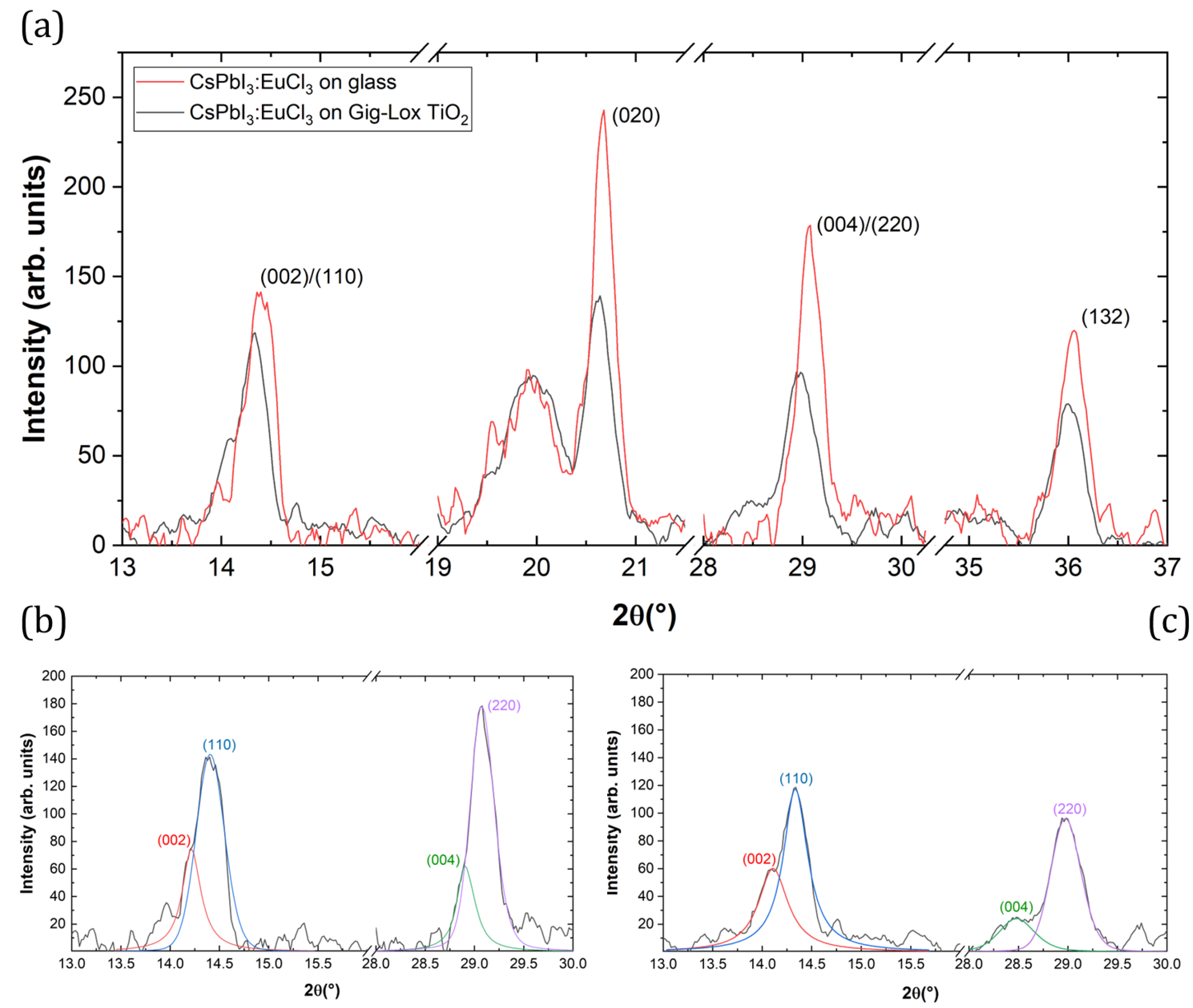
3.2. X-ray Diffraction
3.2.1. Grazing Incidence XRD
3.2.2. Scan
3.3. Spectroscopic Ellipsometry
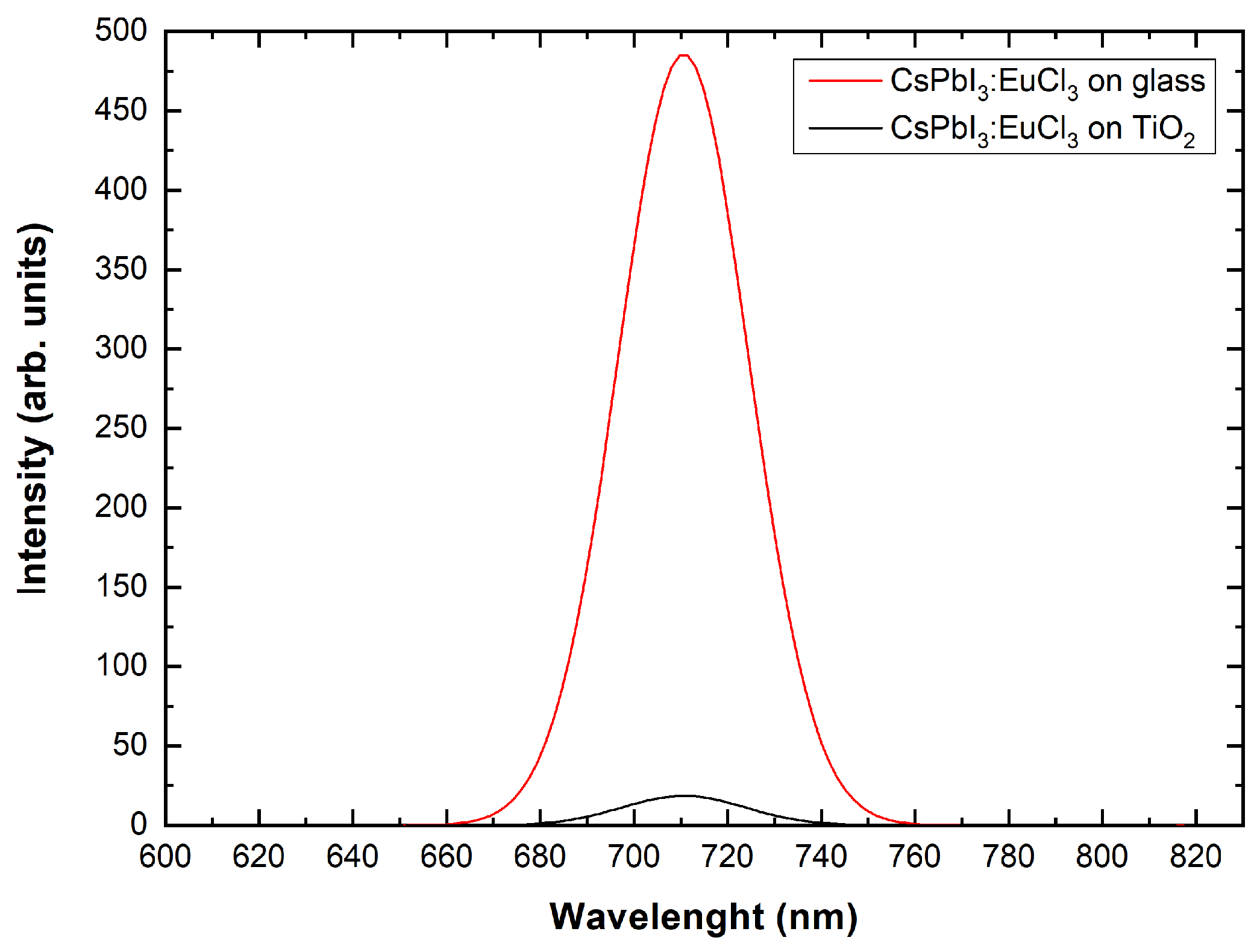
3.4. Photoluminescence Spectroscopy
4. Conclusions
Author Contributions
Funding
Data Availability Statement
Conflicts of Interest
Sample Availability
Abbreviations
| ETL | Electron-transport layer |
| HTL | Hole-transport layer |
| Titanium dioxide | |
| XRD | X-ray diffraction |
| XRR | X-ray reflection |
| GIXRD | Grazing incidence X-ray diffraction |
| DFT | Density functional theory |
| PL | Photoluminescence spectroscopy |
References
- Lenssen, N.J.; Schmidt, G.A.; Hansen, J.E.; Menne, M.J.; Persin, A.; Ruedy, R.; Zyss, D. Improvements in the GISTEMP uncertainty model. J. Geophys. Res. Atmos. 2019, 124, 6307–6326. [Google Scholar] [CrossRef]
- Jain, P. Greenhouse effect and climate change: Scientific basis and overview. Renew. Energy 1993, 3, 403–420. [Google Scholar] [CrossRef]
- The European Commission. REPowerEU Plan; The European Commission: Brussels, Belgium, 2022.
- Čulík, P.; Brooks, K.; Momblona, C.; Adams, M.; Kinge, S.; Maréchal, F.; Dyson, P.J.; Nazeeruddin, M.K. Design and Cost Analysis of 100 MW Perovskite Solar Panel Manufacturing Process in Different Locations. ACS Energy Lett. 2022, 7, 3039–3044. [Google Scholar] [CrossRef]
- National Renewable Energy Laboratory. Best Research-Cell Efficiency Chart. Available online: https://www.nrel.gov/pv/cell-efficiency.html (accessed on 1 November 2023).
- Raval, P.; Kennard, R.M.; Vasileiadou, E.S.; Dahlman, C.J.; Spanopoulos, I.; Chabinyc, M.L.; Kanatzidis, M.; Manjunatha Reddy, G. Understanding instability in formamidinium lead halide perovskites: Kinetics of transformative reactions at grain and subgrain boundaries. ACS Energy Lett. 2022, 7, 1534–1543. [Google Scholar] [CrossRef]
- Lau, C.F.J.; Wang, Z.; Sakai, N.; Zheng, J.; Liao, C.H.; Green, M.; Huang, S.; Snaith, H.J.; Ho-Baillie, A. Fabrication of efficient and stable CsPbI3 perovskite solar cells through cation exchange process. Adv. Energy Mater. 2019, 9, 1901685. [Google Scholar] [CrossRef]
- Montecucco, R.; Quadrivi, E.; Po, R.; Grancini, G. All-inorganic cesium-based hybrid perovskites for efficient and stable solar cells and modules. Adv. Energy Mater. 2021, 11, 2100672. [Google Scholar] [CrossRef]
- Duan, L.; Zhang, H.; Liu, M.; Grätzel, M.; Luo, J. Phase-Pure γ-CsPbI3 for Efficient Inorganic Perovskite Solar Cells. ACS Energy Lett. 2022, 7, 2911–2918. [Google Scholar] [CrossRef]
- Wang, B.; Novendra, N.; Navrotsky, A. Energetics, structures, and phase transitions of cubic and orthorhombic cesium lead iodide (CsPbI3) polymorphs. J. Am. Chem. Soc. 2019, 141, 14501–14504. [Google Scholar] [CrossRef]
- Deretzis, I.; Bongiorno, C.; Mannino, G.; Smecca, E.; Sanzaro, S.; Valastro, S.; Fisicaro, G.; La Magna, A.; Alberti, A. Exploring the structural competition between the black and the yellow phase of CsPbI3. Nanomaterials 2021, 11, 1282. [Google Scholar] [CrossRef]
- Zhang, X.; Yu, Z.; Zhang, D.; Tai, Q.; Zhao, X.Z. Recent Progress of Carbon-Based Inorganic Perovskite Solar Cells: From Efficiency to Stability. Adv. Energy Mater. 2023, 13, 2201320. [Google Scholar] [CrossRef]
- Alberti, A.; Smecca, E.; Deretzis, I.; Mannino, G.; Bongiorno, C.; Valastro, S.; Sanzaro, S.; Fisicaro, G.; Jena, A.K.; Numata, Y.; et al. Formation of CsPbI3γ-Phase at 80 °C by Europium-Assisted Snowplow Effect. Adv. Energy Sustain. Res. 2021, 2, 2100091. [Google Scholar] [CrossRef]
- Valastro, S.; Mannino, G.; Smecca, E.; Sanzaro, S.; Deretzis, I.; La Magna, A.; Jena, A.K.; Miyasaka, T.; Alberti, A. Optical behaviour of γ-black CsPbI3 phases formed by quenching from 80 °C and 325 °C. J. Phys. Mater. 2021, 4, 034011. [Google Scholar] [CrossRef]
- Valastro, S.; Smecca, E.; Bongiorno, C.; Spampinato, C.; Mannino, G.; Biagi, S.; Deretzis, I.; Giannazzo, F.; Jena, A.K.; Miyasaka, T.; et al. Out-of-Glovebox Integration of Recyclable Europium-Doped CsPbI3 in Triple-Mesoscopic Carbon-Based Solar Cells Exceeding 9% Efficiency. Solar RRL 2022, 6, 2200267. [Google Scholar] [CrossRef]
- Cheng, M.; Zuo, C.; Wu, Y.; Li, Z.; Xu, B.; Hua, Y.; Ding, L. Charge-transport layer engineering in perovskite solar cells. Sci. Bull. 2020, 65, 1237–1241. [Google Scholar] [CrossRef]
- Wei, H.; Luo, J.W.; Li, S.S.; Wang, L.W. Revealing the origin of fast electron transfer in TiO2-based dye-sensitized solar cells. J. Am. Chem. Soc. 2016, 138, 8165–8174. [Google Scholar] [CrossRef]
- Chen, K.; Jin, W.; Zhang, Y.; Yang, T.; Reiss, P.; Zhong, Q.; Bach, U.; Li, Q.; Wang, Y.; Zhang, H.; et al. High efficiency mesoscopic solar cells using CsPbI3 perovskite quantum dots enabled by chemical interface engineering. J. Am. Chem. Soc. 2020, 142, 3775–3783. [Google Scholar] [CrossRef] [PubMed]
- Miyasaka, T. Perovskite photovoltaics: Rare functions of organo lead halide in solar cells and optoelectronic devices. Chem. Lett. 2015, 44, 720–729. [Google Scholar] [CrossRef]
- Pihosh, Y.; Turkevych, I.; Ye, J.; Goto, M.; Kasahara, A.; Kondo, M.; Tosa, M. Photocatalytic properties of TiO2 nanostructures fabricated by means of glancing angle deposition and anodization. J. Electrochem. Soc. 2009, 156, K160. [Google Scholar] [CrossRef]
- Chen, S.; Li, Z.; Zhang, Z. Anisotropic TixSn1-xO2 nanostructures prepared by magnetron sputter deposition. Nanoscale Res. Lett. 2011, 6, 1–5. [Google Scholar] [CrossRef] [PubMed]
- Sanzaro, S.; Smecca, E.; Mannino, G.; Bongiorno, C.; Pellegrino, G.; Neri, F.; Malandrino, G.; Catalano, M.R.; Condorelli, G.G.; Iacobellis, R.; et al. Multi-Scale-Porosity TiO2 scaffolds grown by innovative sputtering methods for high throughput hybrid photovoltaics. Sci. Rep. 2016, 6, 39509. [Google Scholar] [CrossRef]
- Valastro, S.; Smecca, E.; Mannino, G.; Bongiorno, C.; Fisicaro, G.; Goedecker, S.; Arena, V.; Spampinato, C.; Deretzis, I.; Dattilo, S.; et al. Preventing lead leakage in perovskite solar cells with a sustainable titanium dioxide sponge. Nat. Sustain. 2023, 6, 974–983. [Google Scholar] [CrossRef]
- Arena, V.; Smecca, E.; Valastro, S.; Bongiorno, C.; Fisicaro, G.; Deretzis, I.; Spampinato, C.; Mannino, G.; Dattilo, S.; Scamporrino, A.A.; et al. Lead Detection in a Gig-Lox TiO2 Sponge by X-ray Reflectivity. Nanomaterials 2023, 13, 1397. [Google Scholar] [CrossRef] [PubMed]
- Spampinato, C.; La Magna, P.; Valastro, S.; Smecca, E.; Arena, V.; Bongiorno, C.; Mannino, G.; Fazio, E.; Corsaro, C.; Neri, F.; et al. Infiltration of CsPbI3: EuI2 Perovskites into TiO2 Spongy Layers Deposited by gig-lox Sputtering Processes. Solar 2023, 3, 347–361. [Google Scholar] [CrossRef]
- Sanzaro, S.; Zontone, F.; Grosso, D.; Bottein, T.; Neri, F.; Smecca, E.; Mannino, G.; Bongiorno, C.; Spinella, C.; La Magna, A.; et al. Bimodal porosity and stability of a TiO2 gig-lox sponge infiltrated with methyl-ammonium lead iodide perovskite. Nanomaterials 2019, 9, 1300. [Google Scholar] [CrossRef]
- Wu, J.; Liu, S.C.; Li, Z.; Wang, S.; Xue, D.J.; Lin, Y.; Hu, J.S. Strain in perovskite solar cells: Origins, impacts and regulation. Natl. Sci. Rev. 2021, 8, nwab047. [Google Scholar] [CrossRef]
- Spampinato, C.; Valastro, S.; Smecca, E.; Arena, V.; Mannino, G.; La Magna, A.; Corsaro, C.; Neri, F.; Fazio, E.; Alberti, A. Spongy TiO2 layers deposited by gig-lox sputtering processes: Contact angle measurements. J. Vac. Sci. Technol. 2023, 41, 012802. [Google Scholar] [CrossRef]
- Pietsch, U.; Holy, V.; Baumbach, T. High-Resolution X-ray Scattering: From Thin Films to Lateral Nanostructures; Springer Science & Business Media: Berlin/Heidelberg, Germany, 2004. [Google Scholar]
- Dimitrievska, M.; Fairbrother, A.; Gunder, R.; Gurieva, G.; Xie, H.; Saucedo, E.; Pérez-Rodríguez, A.; Izquierdo-Roca, V.; Schorr, S. Role of S and Se atoms on the microstructural properties of kesterite Cu2ZnSn (SxSe1-x)4 thin film solar cells. Phys. Chem. Chem. Phys. 2016, 18, 8692–8700. [Google Scholar] [CrossRef]
- Hubbell, J.H.; Seltzer, S.M. Tables of X-ray Mass Attenuation Coefficients and Mass Energy-Absorption Coefficients 1 keV to 20 MeV for Elements Z = 1 to 92 and 48 Additional Substances of Dosimetric Interest; Technical Report, National Inst. of Standards and Technology-PL; Ionizing Radiation Div.: Gaithersburg, MD, USA, 1995. [Google Scholar]
- Parratt, L.G. Surface studies of solids by total reflection of X-rays. Phys. Rev. 1954, 95, 359. [Google Scholar] [CrossRef]
- Patterson, A. The Scherrer formula for X-ray particle size determination. Phys. Rev. 1939, 56, 978. [Google Scholar] [CrossRef]
- Bragg, W.H.; Bragg, W.L. The reflection of X-rays by crystals. Proc. R. Soc. Lond. Ser. Contain. Pap. Math. Phys. Character 1913, 88, 428–438. [Google Scholar] [CrossRef]
- Kelly, A.; Knowles, K.M. Crystallography and Crystal Defects; John Wiley & Sons: Hoboken, NJ, USA, 2020. [Google Scholar]
- Sutton, R.J.; Filip, M.R.; Haghighirad, A.A.; Sakai, N.; Wenger, B.; Giustino, F.; Snaith, H.J. Cubic or orthorhombic? Revealing the crystal structure of metastable black-phase CsPbI3 by theory and experiment. ACS Energy Lett. 2018, 3, 1787–1794. [Google Scholar] [CrossRef]
- Meng, W.; Zhang, K.; Osvet, A.; Zhang, J.; Gruber, W.; Forberich, K.; Meyer, B.; Heiss, W.; Unruh, T.; Li, N.; et al. Revealing the strain-associated physical mechanisms impacting the performance and stability of perovskite solar cells. Joule 2022, 6, 458–475. [Google Scholar] [CrossRef]
- Kim, H.S.; Park, N.G. Importance of tailoring lattice strain in halide perovskite crystals. NPG Asia Mater. 2020, 12, 78. [Google Scholar] [CrossRef]
- Jones, T.W.; Osherov, A.; Alsari, M.; Sponseller, M.; Duck, B.C.; Jung, Y.K.; Settens, C.; Niroui, F.; Brenes, R.; Stan, C.V.; et al. Lattice strain causes non-radiative losses in halide perovskites. Energy Environ. Sci. 2019, 12, 596–606. [Google Scholar] [CrossRef]


| Grazing Angle (°) | Penetration Depth (nm) | Penetration Depth (nm) Anatase Blend |
|---|---|---|
| 0.2° | 3.49 | 3.86 |
| 0.3° | 14.68 | 25.77 |
| 0.4° | 37.28 | 56.84 |
| 0.6° | 70.45 | 104.37 |
| 0.8° | 98.97 | 145.77 |
| Scan Angle (°) | FWHM (°) | Crystallite Size (nm) | FWHM (°) | Crystallite Size (nm) | ||
|---|---|---|---|---|---|---|
| 0.2° | Glass Substrate | 0.274 | 30.49 | Gig-Lox Substrate | 0.214 | 39.94 |
| 0.3° | 0.312 | 26.56 | 0.271 | 30.85 | ||
| 0.4° | 0.251 | 33.51 | 0.289 | 28.80 | ||
| 0.6° | 0.271 | 30.85 | 0.28 | 29.79 | ||
| 0.8° | 0.253 | 33.22 | 0.293 | 28.38 |
| Miller Index | Angle (°) | d (A) | Crystallite Sizes (nm) | Intensity | Angle (°) | d (A) | Crystallite Sizes (nm) | Intensity | ||
|---|---|---|---|---|---|---|---|---|---|---|
| (002) | Glass substrate | 14.21 | 6.228 | 40.65 | 73.7 | substrate | 14.10 | 6.275 | 24.43 | 60.1 |
| (110) | 14.41 | 6.143 | 25.81 | 139.1 | 14.33 | 6.174 | 29.99 | 117 | ||
| (020) | 20.66 | 4.295 | 35.50 | 242.4 | 20.63 | 4.302 | 27.20 | 139.4 | ||
| (120) | 23.09 | 3.848 | 30.73 | 108.5 | 23.06 | 3.854 | 30.25 | 73.0 | ||
| (121) | 24.17 | 3.680 | 23.34 | 103.7 | 24.14 | 3.684 | 26.02 | 84.9 | ||
| (004) | 28.90 | 3.087 | 50.13 | 36.3 | 28.47 | 3.132 | 21.38 | 24.6 | ||
| (220) | 29.08 | 3.068 | 32.51 | 178.9 | 28.97 | 3.079 | 25.28 | 96.5 | ||
| (130) | 32.96 | 2.715 | 28.10 | 65.1 | 32.92 | 2.719 | 28.30 | 46.1 | ||
| (131) | 33.57 | 2.667 | 19.51 | 36.0 | n.a. | n.a. | n.a. | n.a. | ||
| (132) | 36.05 | 2.490 | 29.15 | 115 | 36 | 2.493 | 26.66 | 79.3 |
| Lattice Parameters of the Orthorhombic -Phase | This Work Spin Coated Layers Quenched from 350 °C Using Eu Glass Substrate | This Work Spin Coated Layers Quenched from 350 °C Using Eu Blended Material | Sutton et al. Powder Fast Quenched from 347 °C in [36] |
|---|---|---|---|
| a [Å] | 8.790 | 8.875 | 8.856 |
| b [Å] | 8.581 | 8.580 | 8.577 |
| c [Å] | 12.433 | 12.545 | 12.472 |
| Unit cell [Å] | 937.78 | 955.27 | 947.33 |
Disclaimer/Publisher’s Note: The statements, opinions and data contained in all publications are solely those of the individual author(s) and contributor(s) and not of MDPI and/or the editor(s). MDPI and/or the editor(s) disclaim responsibility for any injury to people or property resulting from any ideas, methods, instructions or products referred to in the content. |
© 2023 by the authors. Licensee MDPI, Basel, Switzerland. This article is an open access article distributed under the terms and conditions of the Creative Commons Attribution (CC BY) license (https://creativecommons.org/licenses/by/4.0/).
Share and Cite
La Magna, P.; Spampinato, C.; Valastro, S.; Smecca, E.; Arena, V.; Mannino, G.; Deretzis, I.; Fisicaro, G.; Bongiorno, C.; Alberti, A. X-ray Investigation of CsPbI3:EuCl3 Infiltrated into Gig-Lox TiO2 Spongy Layers for Perovskite Solar Cells Applications. Nanomaterials 2023, 13, 2910. https://0-doi-org.brum.beds.ac.uk/10.3390/nano13222910
La Magna P, Spampinato C, Valastro S, Smecca E, Arena V, Mannino G, Deretzis I, Fisicaro G, Bongiorno C, Alberti A. X-ray Investigation of CsPbI3:EuCl3 Infiltrated into Gig-Lox TiO2 Spongy Layers for Perovskite Solar Cells Applications. Nanomaterials. 2023; 13(22):2910. https://0-doi-org.brum.beds.ac.uk/10.3390/nano13222910
Chicago/Turabian StyleLa Magna, Paola, Carlo Spampinato, Salvatore Valastro, Emanuele Smecca, Valentina Arena, Giovanni Mannino, Ioannis Deretzis, Giuseppe Fisicaro, Corrado Bongiorno, and Alessandra Alberti. 2023. "X-ray Investigation of CsPbI3:EuCl3 Infiltrated into Gig-Lox TiO2 Spongy Layers for Perovskite Solar Cells Applications" Nanomaterials 13, no. 22: 2910. https://0-doi-org.brum.beds.ac.uk/10.3390/nano13222910