
Quantitatively Exploring Giant Optical Anisotropy of Quasi-One-Dimensional Ta2NiS5


1
State Key Laboratory of Intelligent Manufacturing and Technology, Huazhong University of Science and Technology, Wuhan 430074, China
2
Guangdong Provincial Key Laboratory of Manufacturing Equipment Digitization, Guangdong HUST Industrial Technology Research Institute, Dongguan 523003, China
3
Optics Valley Laboratory, Wuhan 430074, China
4
Wuhan China Star Optoelectronics Semiconductor Display Technology Co., Ltd., Wuhan 430078, China
*
Author to whom correspondence should be addressed.
Nanomaterials 2023, 13(24), 3098; https://0-doi-org.brum.beds.ac.uk/10.3390/nano13243098
Submission received: 4 November 2023
/
Revised: 1 December 2023
/
Accepted: 4 December 2023
/
Published: 7 December 2023
(This article belongs to the Special Issue Optical Spectroscopy Characterizations of Low-Dimensional Nanomaterials)
Abstract
:Optical anisotropy offers a heightened degree of flexibility in shaping optical properties and designing cutting-edge devices. Quasi-one-dimensional Ta2NiS5, with giant optical anisotropy, has been used in the development of new lasers and sensors. In this research endeavor, we successfully acquired the complete dielectric tensor of Ta2NiS5, utilizing the advanced technique of Mueller matrix spectroscopic ellipsometry, enabling a rigorous quantitative assessment of its optical anisotropy. The results indicate that Ta2NiS5 demonstrates giant birefringence and dichroism, with Δnmax = 1.54 and Δkmax = 1.80. This pursuit also delves into the fundamental underpinnings of this optical anisotropy, drawing upon a fusion of first-principles calculations and critical points analysis. The anisotropy of Ta2NiS5 arises from differences in optical transitions in different directions and is shown to be due to van Hove singularities without exciton effects. Its giant optical anisotropy is expected to be useful in the design of novel optical devices, and the revelation of the physical mechanism facilitates the modulation of its optical properties.
1. Introduction
Two-dimensional (2D) or quasi-one-dimensional (quasi-1D) materials with in-plane anisotropy, such as PdSe2 [1], ReS2 and ReSe2 [2,3], ZrTe5 [4], CrPS4 [5], TiS3 and ZrS3 [6], have been hot topics in research since the study of black phosphorus (BP) [7,8,9]. These types of materials not only exhibit richer physical properties, but also provide an additional degree of freedom to modulate physical properties [10], leading to the design of novel electronic, optical, thermal, and optoelectronic devices, a feature that is not available in isotropic materials. In recent years, the exploration of new applications for low-dimensional materials has triggered extensive research into their optical anisotropy [11,12]. However, it is worth noting that most of the studies have focused on the qualitative observation and exploration of optical anisotropy phenomena, as well as designing devices based on characterization and experience. Quantitative measurements of optical anisotropy and the intrinsic formation mechanisms have not received significant attention.
The optical anisotropy of low-dimensional materials is usually described quantitatively using the dielectric tensor [13,14]. The different elements of the dielectric tensor provide quantitative information about the response of a material to electric fields in different directions, which helps to understand and predict the optical behavior of anisotropic materials for the design and optimization of optical and electronic devices. Therefore, the measurement of the complete dielectric tensor is of great significance in anisotropic materials research and applications. In addition, the physical formation mechanism of the characteristic spectral absorption structures of the dielectric function spectrum needs to be explored urgently, which will help to analyze and explain the mechanism of optical anisotropy.
Currently, techniques for determining the dielectric tensor of anisotropic materials include reflection-based methods [15], scattering-type scanning near-field optical microscopy (s-SNOM) based on near-field imaging [16,17,18], and polarization-based ellipsometry [19,20,21]. Conventional reflection-based methods generally need to be combined with the Kramers-Kronig (K-K) relations to obtain the dielectric tensor [22,23]. This method leads to inaccurate dielectric tensor measurements due to the fact that the wavelength measurement range of the instrument cannot reach infinity, and the K-K relations need to be approximated [24]. s-SNOM can accurately obtain the dielectric tensor of uniaxial crystals, but measurements of biaxial crystals need to be made with the help of other techniques to determine the position of the in-plane principal axes first [16]. Mueller matrix spectroscopic ellipsometry (MMSE) [25,26,27], on the other hand, can obtain the dielectric tensor accurately and completely and does not require a priori knowledge of thickness or crystal axis orientation [28,29,30]. A systematic approach based on first-principles calculations and critical points analysis [31] can be used to reveal the correlation between the absorption peaks of the dielectric function and the optical transitions [4,20,32], including the center energy of the transitions, their positions in the Brillouin zone (BZ), the energy bands involved in the transitions, and the types of carriers; additionally, the optical transitions analysis along different directions can reveal the physical origin of the optical anisotropy.
The quasi-one-dimensional dimetallic sulfide Ta2NiS5 has attracted much attention in recent years as an emerging low-dimensional material [33,34,35]. Ta2NiS5 has great potential as a broadband saturable absorber [36] for applications, such as infrared lasers [37,38,39,40], sensors [41], and photodetectors [42]. Its electrical and thermal anisotropy have been reported successively [43,44], and it exhibits a giant optical anisotropy; thus it may have promising prospects for applications in polarization devices, nonlinear optics, and sensors.
In this work, we use MMSE to accurately obtain the complete dielectric tensor of quasi-one-dimensional Ta2NiS5 over a wide spectral range of the UV-Vis-NIR (193 nm–1690 nm) and combine it with first-principles calculations and critical points analyses to quantitatively study its giant optical anisotropy in depth. Raman spectroscopy is used to characterize the structural information of the Ta2NiS5 sample. Angle-Resolved Raman Spectroscopy, polarization-resolved reflectance spectroscopy, and azimuthally resolved MMSE spectroscopy measurements qualitatively demonstrate its optical anisotropy, and the full permittivity tensor of Ta2NiS5 is obtained by constructing a simulation of the combined MMSE spectra. The critical points analysis of the absorption transitions corresponding to the characteristic peaks of the dielectric function and the energy band structure and the density of joint states of Ta2NiS5 are calculated by combining with the first nature principle, which reveals the physical formation mechanism of the optical anisotropy.
2. Materials and Methods
2.1. Preparation and Characterization of Ta2NiS5 Single Crystals
High-quality Ta2NiS5 single crystals were purchased from Shanghai Onway Technology Co., Ltd., Shanghai, China (link: onway-tec.com accessed on 1 October 2023) These samples are prepared using the chemical vapor transport (CVT) method from high-purity raw materials and can be up to millimeters in size. The LabRAM HR800 (HORIBA Jobin Yvon, Paris, France; link: horiba.com accessed on 2 November 2023) laser confocal Raman spectrometer was used to characterize the quasi-one-dimensional structure of Ta2NiS5 and observe its optical anisotropy phenomena. A micro-UV-visible near-infrared spectrophotometer (Jasco MSV-5200, JASCO Corporation, Tokyo, Japan; link: jascoinc.com accessed on 2 November 2023) and a commercial Muller matrix spectroscopic ellipsometer (MMSE, ME-L Mueller matrix spectroscopic ellipsometry, Wuhan E-optics Technology Co., Ltd., Wuhan, China; link: eoptics.com.cn accessed on 14 July 2023) were also employed to qualitatively characterize the anisotropy of Ta2NiS5. The MMSE was also used to obtain the Muller matrix spectra at room temperature with its 200 μm probing spot and ulteriorly acquire the complete dielectric tensor. In addition, the CCD camera on the MMSE helps to determine the measurement position on the sample at the same point.
2.2. First-Principles Calculations
All calculations were performed with the Vienna Ab initio Simulation Package (VASP v5.4.4). The Perdew–Burke–Ernzerhof (PBE) functional of generalized gradient approximation (GGA) based on the projected augmented wave (PAW) pseudopotentials was used to describe the exchange correlation potential. In the optimization of geometric structure, we used the PBE functional based on PAW pseudopotential, with an energy cutoff of 400 eV and an 8 × 8 × 2 Г-centered k-point mesh. When calculating the projected density of states (PDOS), a denser 16 × 16 × 4 Г-centered k-point mesh was used. The convergence criterion of force is 0.01 eV/Å and of total energy is 10−5 eV. The effect of spin–orbit coupling (SOC) was considered in all calculations.
3. Results and Discussion
3.1. Quasi-One-Dimensional Structure and Optical Anisotropy of Ta2NiS5
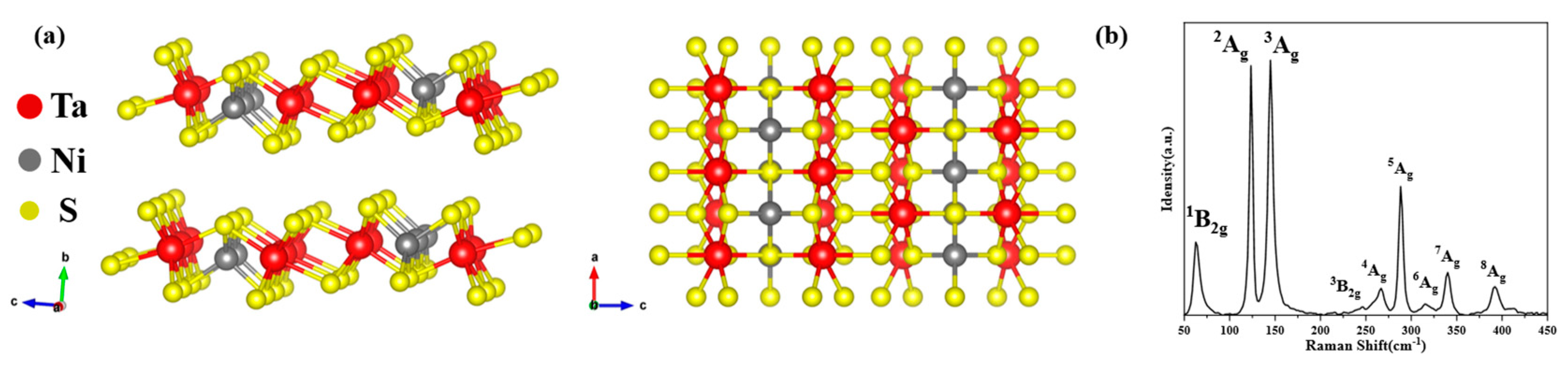
Ta2NiS5 is a ternary chalcogenide compound with a typical van der Waals layered structure, belonging to the orthorhombic system (Cmcm space group, lattice constant a = 3.415 Å, b = 12.146 Å, c = 15.097 Å) at room temperature [33,35,45]. Figure 1a shows its quasi-one-dimensional structure. In the a-c plane, Ni and Ta atoms are combined with S atoms to form a Ni-S4 tetrahedron and Ta-S6 octahedron, respectively. Ni-S4 tetrahedrons and Ta-S6 octahedrons are each combined into linear chains along the a-axis and arranged into planes in the manner of two Ta-S6 octahedron chains per one Ni-S4 tetrahedron chain along the c-axis [35]. This different atomic arrangement of Ta2NiS5 along the a-axis and c-axis also predicts its giant in-plane optical anisotropy. The experimental bulk sample is long and oriented along the long strip in the a-axis, which is related to its chain structure along the a-axis, which we verified later through the results of first-principles calculations. Figure 1b shows the Raman spectrum of the bulk Ta2NiS5, showing 7 Ag modes (2Ag: 123.6 cm−1, 3Ag: 145.1 cm−1, 4Ag: 266.3 cm−1, 5Ag: 288.7 cm−1, 6Ag: 317.2 cm−1, 7Ag: 340.1 cm−1, 8Ag: 392.6 cm−1) and 2 B2g modes (1B2g: 63.8 cm−1, 3B2g: 262.1 cm−1). Previous studies have shown that Ta2NiS5 has 8 Ag modes and 3 B2g modes [33,46], which matches the measurements in Figure 1b, confirming the structure of the bulk sample. It should be noted that the 1Ag mode is less than 50 cm−1, which is beyond the measurement range of the instrument, and the 2B2g mode is between 2Ag and 3Ag, which cannot be visualized due to the small intensity of 2B2g and the high intensity of 2Ag and 3Ag.
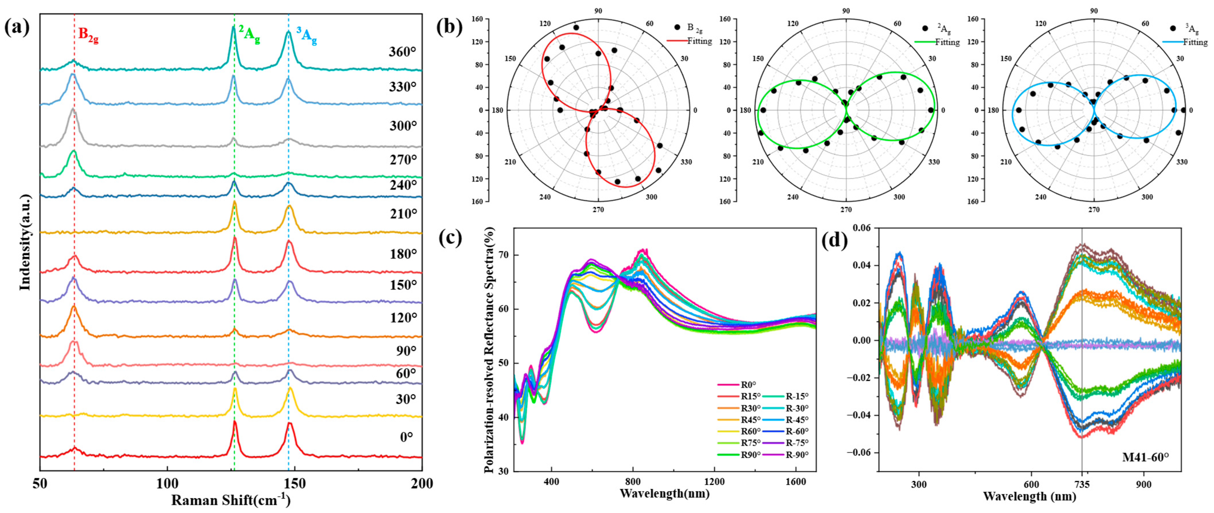
The optical anisotropy of Ta2NiS5 was observed using angle-resolved Raman spectroscopy, as shown in Figure 2a (three Raman modes 1B2g [in other words, the following B2g], 2Ag, and 3Ag, were chosen here as representatives, and their vibrational modes are shown in Figure S1). With the change in Raman laser polarization direction, the angle between the laser electric field direction and the crystal optical axis direction is changed, resulting in a periodic change in the Raman scattered light intensity for all of the different modes, of which the polar plots of the light intensity for the B2g, 2Ag and 3Ag three vibrational modes are shown in Figure 2b. We theoretically calculated the Raman intensity [47] versus angle change (see Supplementary Materials), which showed that the curve in Figure 2b and the theoretical calculation results are in good agreement with the experimental results.
In addition, we also measured the reflectance of Ta2NiS5 using a micro-distinguished photometer, as shown in Figure 2c, which also showed significant differences in reflectance under the change in polarization angle from −90° to 90°, which is related to the relative positions of the optical axis direction and the polarization direction. In these data, R0° corresponds to the a-axis direction Ra and R90°/−90° to the c-axis direction Rc.
MMSE is a non-contact measuring instrument widely used to characterize the thickness and optical properties of nanomaterials. It generates polarized light through the polarizing arm and detects the change in the polarized light in the detector arm after reflection from the sample, thus obtaining the properties of the material. Unlike conventional ellipsometry, it can measure the generalized ellipsometric parameters (the 15 components of the 4 × 4 normalized Mueller matrix), which can be converted into the 2 × 2 Jones matrix when the depolarization effect is neglected. It should be noted that the Mueller matrices obtained from the measurements in this work are all normalized. The off-diagonal elements of the Mueller matrix reflect the anisotropy of the material, and the spectrum of one of the off-diagonal elements of the Mueller matrix, M41, at an incident angle of 60° is shown in Figure 2d. For the experiments, we placed the a-axis of the bulk sample parallel to the x-axis of the ellipsometric coordinate system when the azimuth angle was 0°, which helped to simplify the rotation of the coordinate system during the ellipsometric analysis. The values of the off-diagonal elements of the Mueller matrix are affected by both the magnitude of the anisotropy of the material and the orientation of the optical axis of the sample during the measurement. Thus, we observed the changes in the M41 values by rotating the sample in the a-c plane to change the orientation of the optical axis; this angle of rotation is called the ellipsometric azimuth angle (Figure S5). The azimuths of the curves of the same color in Figure 2d differ by 180°, and it can be seen that the values of the element M41 at the same wavelength such as 735 nm show a clear periodicity.
3.2. Quantitative Characterization of the Optical Anisotropy of Ta2NiS5
The complete Mueller matrix spectrum acquired by MMSE was used to extract the dielectric tensor. This process was realized by building a reasonable optical model that includes a suitable dispersion model composed of several contributions describing individual absorption structures to match the spectrum of the Mueller matrix. The individual contributions were modeled using the Tauc–Lorentz model [48] or using the model of Gaussian broadened harmonic oscillators (a Gaussian curve for ε2, and an ε1 curve that maintains Kramers–Kronig agreement [49]). We used the root mean square error RMSE to quantitatively evaluate how well the fitted data matched the experimental data, defined as [4]:
where Mci,j and Mmi,j denote the calculated and measured values of the Mueller matrix, the subscript i,j denotes the ith row and the jth column, L, l denotes the total number of points and the lth point of the measurement, and h denotes the number of fitted parameters. In general, a smaller RMSE indicates a better fit, and a good model should have an RMSE of less than 10.
The Ta2NiS5 sample in our experiments was bulk. It reaches a thickness of several hundred micrometers, in which the dielectric shielding effect is weak, and there is no need to consider the effect of thickness on optical properties. Therefore, the optical model was built by treating it directly as a substrate to analyze; in other words, only the optical constants of the sample (and not the thickness of the sample) were fitted. The fitting results show RMSE = 7.795 (more details in Supplementary Materials), which indicates that the optical constants obtained have a fairly high accuracy and verifies our rationale for analyzing the bulk sample as a substrate.
For an orthorhombic crystal such as Ta2NiS5, the dielectric tensor is a 3rd-order diagonal matrix, with the main diagonal elements being the dielectric function in the direction of each of the three crystal axes, and containing one real and one imaginary part each:
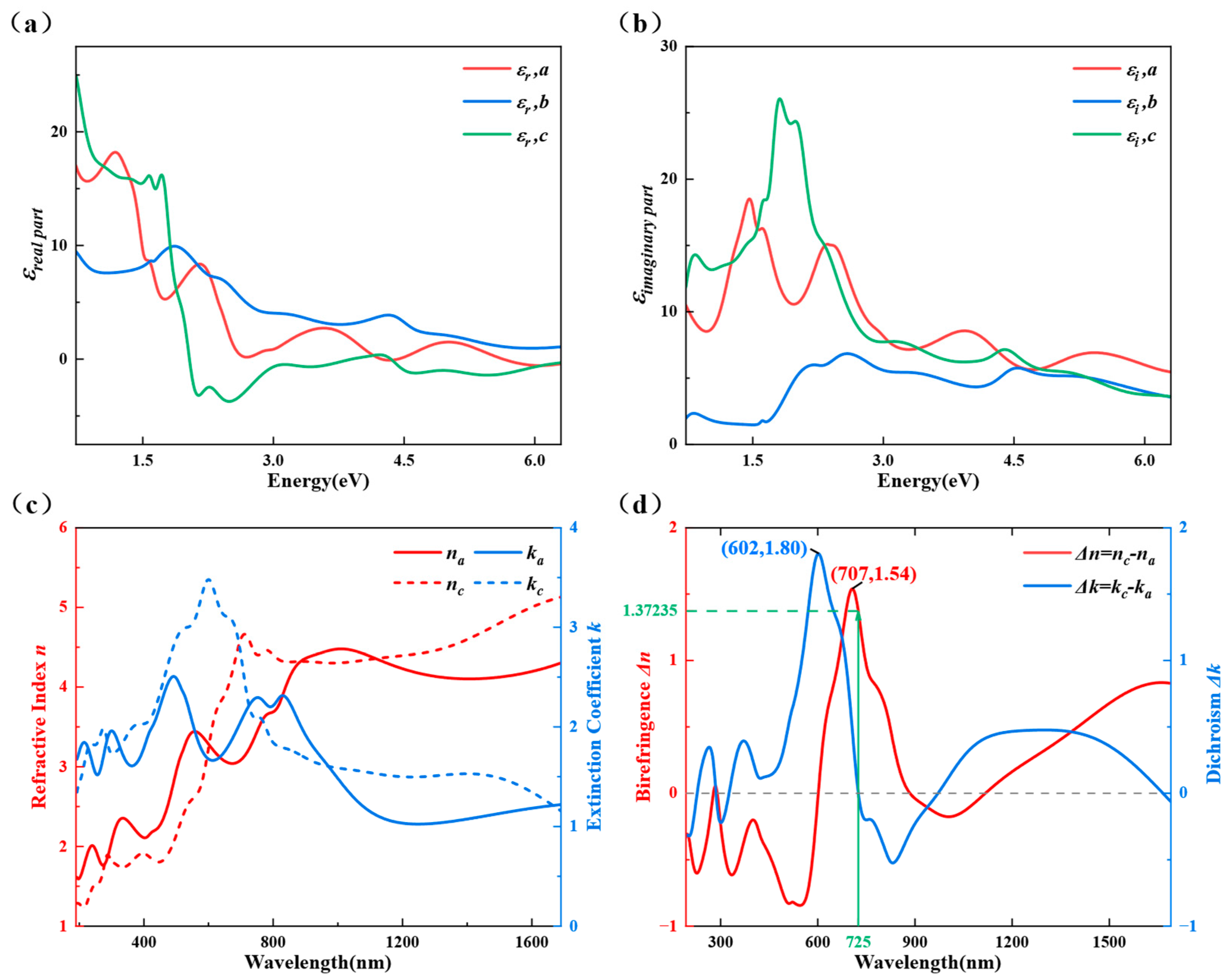
Figure 3a,b show the real and imaginary parts of the dielectric function of Ta2NiS5 obtained by fitting the Mueller matrix. There is a large difference between the dielectric functions of the three crystal axes. The difference in the b-axis, which is bonded by van der Waals forces along the interlayer direction, is particularly obvious compared to the a- and c-axes, whereas the a-c plane is bonded by the covalent bonds of Ta-S and Ni-S. The differences between a- and c-axes are thought to be due to the different atomic arrangements resulting from quasi-one-dimensional chain structures, causing different quantities and rows of the two kinds of covalent bonds in the two directions. In the complex refractive index, Nx = nx − ikx = , where the subscript x denotes the three crystal axes of the orthorhombic crystal system a, b and c, n is the refractive index and k is the extinction coefficient. The complex refractive index tensor is calculated from the dielectric tensor, as shown in Figure 3c. The in-plane anisotropy is expected to be used in the design of new devices, so only the complex refractive indices for the a-axis and c-axis are given here. The n and k in both directions are very different in both their waveform and amplitude, quantitatively showing the giant optical anisotropy of Ta2NiS5.
The in-plane anisotropy is often quantitatively described by two parameters: birefringence Δn = nc − na and dichroism Δk = kc − ka [50,51]. These parameters can be calculated from the previously obtained in-plane complex refractive indices, as shown in Figure 3d. The absolute values of birefringence and dichroism are mostly higher than 0.2 in the measured wavelength range and even exceed 1 in some wavelength ranges, which is a good indication that its optical anisotropy is giant. In the measured wavelength range, there is maximum birefringence Δnmax = 1.54 at a wavelength of 707 nm and maximum dichroism Δkmax = 1.80 at a wavelength of 602 nm. And at a wavelength of 725 nm, the birefringence Δn = 1.37 and the dichroism Δk = 0 are expected to be used for designing waveplates. Compared with some other low-dimensional materials and waveplate materials, such as BP [52] and rutile [53], its giant optical anisotropy has an obvious advantage, and it has great potential in realizing the miniaturization and integration of optical devices.
The complex refractive index can also be used to calculate the reflectance of orthorhombic crystal systems such as Ta2NiS5 [13]:
where the subscript m denotes the three crystal axes of the orthorhombic crystal system a, b, c, and R, n, and k represent the reflectance, refractive index, and extinction coefficient in this direction, respectively. After obtaining the complex refractive index, its reflectance was calculated using Equation (3) and verified by experimental measurements (Figure S5). The calculated reflectance matches well with the actual measured reflectance, especially at the peak and valley positions. Even some inconspicuous peaks are reflected in the theoretically calculated reflectance. This proves the accuracy and reliability of our complex refractive index obtained by MMSE from the side. In addition, the optical constants obtained from the first nature principles calculation of the optical properties of Ta2NiS5 are also in high agreement with those obtained experimentally, (Figure S6), which, likewise, validates our experimental results.
3.3. Critical Points and Optical Transitions
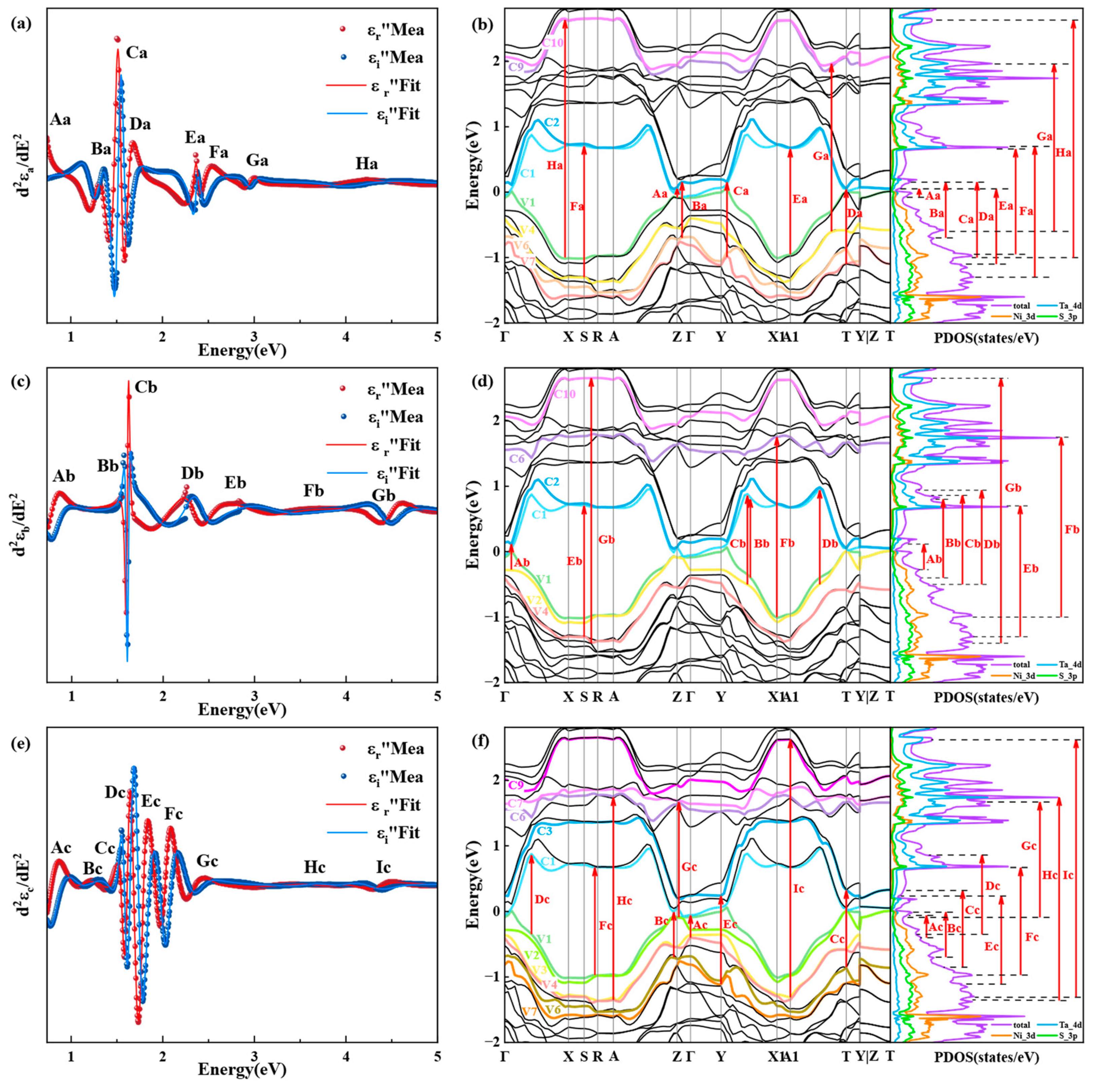
In order to better comprehend the giant optical anisotropy of Ta2NiS5, we performed critical points (CP) and optical transitions analysis of its dielectric function in the three crystal axis directions. Critical points analysis is performed by varying different parameters of the critical points to fit the second-order partial derivatives of the dielectric function with respect to energy [31]:
where A, ϕ, E0, and Г denote the amplitude, phase, center energy, and damping coefficient of the critical points, respectively, i is an imaginary unit, and n denotes the dimensions of the optical transitions involved in the critical points (including three-dimensional, two-dimensional, one-dimensional, and zero-dimensional), and the corresponding n is 1/2, 0, −1/2, and −1, respectively. More details about CP analysis can be found in the Supplementary Materials. Figure 4a,c,e show the second-order derivatives of the nodal functions with respect to the energy d2ε/dE2 and their best-fit curves for each of the three directions. There are 9, 9, and 11 0D critical points along the a-axis, b-axis, and c-axis directions in the measured spectral region, from which the center energy of the corresponding optical transitions is determined, and the parameters related to the CP points are detailed in Table S2. The energy band structure and PDOS obtained from first-principles calculations can be linked to the CP points. As shown in Figure 4b,d,f, the center energy value of the CP points is used to identify where its optical transitions occur in the energy band structure and to recognize its carrier type in the PDOS.
For Ta2NiS5, there is a large no-band range between the twelfth and thirteenth low guide bands, and electrons in lower valence bands are more difficult to excite; thus, only optical transitions below 4.5 eV are considered. In Figure 4b, the critical point Aa with a center energy E0 of 0.53 eV (in other words, Ec-v = E0 = 0.53 eV) represents the optical transition from V1 to C1 located at the high-symmetry point Z in the Brillouin zone. The critical point Ba (E0 = 1.25 eV) indicates the optical transition from V6 to C2 between points Z and Γ in the Brillouin zone. The critical point Ca (E0 = 1.53 eV) appears in k-space between the points Y and X1, corresponding to the optical transition from V7 to C2. There are three critical points Da (E0 = 1.55 eV), Ea (E0 = 2.38 eV), and Fa (E0 = 2.40 eV) at the high-symmetry points T, A1, and S in the Brillouin zone, corresponding to the optical transitions from V7 to C2, from V1 to C2, and from V4 to C1, respectively. The critical point Ga (E0 = 2.97 eV) denotes the transition from V4 to C10 located between the points T and A1, and Ha (E0 = 4.05 eV) denotes the transition from V1 to C9 located between points Γ and X. Similarly, we can obtain the results of the optical transitions analysis for the b and c axes, as shown in Table 1.
The electronic transitions corresponding to the critical points in the three crystal axis directions show significant differences, in terms of both k-space position and energy bands involved, which is the physical explanation for the generation of the anisotropy of the dielectric function. In particular, the a-axis and c-axis directions have critical points at two identical locations in k-space at points A1 and T, suggesting that electrons here are involved in dielectric activity in both directions. In addition, the best fit of the 0D critical points illustrates the deeply localized character of the Ta2NiS5 electron wavefunction [54]. In other words, the optical transitions are dominated by multiple van Hove singularities rather than delocalized excitons [55], which matches previous reports [43,54]. Additionally, all critical points are caused by electrons in the valence band consisting of hybridized Ni-3d and S-3p orbitals transitioning as main carriers to the conduction band formed by the Ta-5d orbital.
4. Conclusions
In summary, this investigation quantitatively analyzes the complete dielectric tensor of quasi-one-dimensional Ta2NiS5 in the UV-Vis-NIR spectral range, examines its giant optical anisotropy, and probes the physical origin of the anisotropy in conjunction with CP analysis and first-principles calculations. Angle-resolved Raman spectroscopy, polarization-resolved reflectance spectroscopy, and azimuthally resolved Mueller matrix spectroscopy qualitatively observe the optical anisotropy phenomenon in Ta2NiS5. The dielectric tensor of Ta2NiS5 over a wide spectral range is determined by MMSE, and accurate numerical curves of its birefringence and dichroism are obtained, which provide data support for possible device design, and its giant optical anisotropy is of great advantage and prospect in realizing the miniaturization and integration of polarized optics devices. The CP analysis and the optical transitions analysis show, from a quantum mechanical point of view, that the fundamental reason for the differences in the properties of the three crystal axis orientations of Ta2NiS5 is the differences in the optical transitions corresponding to the CPs. It is also shown that Ta2NiS5 does not exhibit delocalized exciton transitions but rather has multiple van Hove singularities. Our work provides data and physical mechanisms for the regulation of optical properties of Ta2NiS5, enriches the database of optical constants of materials, and facilitates the further study and application of quasi-one-dimensional Ta2NiS5.
Supplementary Materials
The following supporting information can be downloaded at: https://0-www-mdpi-com.brum.beds.ac.uk/article/10.3390/nano13243098/s1, Figure S1. Schematic illustration of atomic displacements in the three vibration modes. Figure S2. Schematic diagram of Raman measurement experiment. Figure S3a. Schematic diagram of Mueller matrix ellipsometry principle. Figure S3b. Schematic diagram of an ellipsometry experiment. Figure S4. Mueller matrix spectra of Ta2NiS5 with incidence angles from 55° to 70° and their best-fit curves. Figure S5. Experimental and calculated reflectance spectra of a-axis and c-axis. Figure S6. Optical constants calculated from first principles. Table S1. Best-fit parameters for physical oscillators in anisotropic ellipsometric fitting. Table S2. Best-fit parameters for Ta2NiS5 critical points analysis. Refs. [4,33,46,47] are cited in the Supplementary Materials.
Author Contributions
Q.Z. and H.G. conceived the idea; Q.Z., Z.G. and K.D. performed the theory calculations and numerical simulations, analyzed and visualized the data, and prepared the original manuscript; Z.G., S.L., H.G. and K.D. wrote, reviewed and edited the manuscript; S.L. and H.G. supervised the project. All authors have read and agreed to the published version of the manuscript.
Funding
This work was funded by the National Key Research and Development Plan of China (Grant No. 2022YFB2803900), National Natural Science Foundation of China (Grant No. 52130504), Guangdong Basic and Applied Basic Research Foundation (Grant No. 2023A1515030149), Key Research and Development Program of Hubei Province (Grant No. 2021BAA013), the Innovation Project of Optics Valley Laboratory (Grant No. OVL2023PY003), and the Fundamental Research Funds for the Central Universities (Grant No. 2021XXJS113). The authors thank the technical support from the Experiment Centre for Advanced Manufacturing and Technology in School of Mechanical Science & Engineering of HUST.
Data Availability Statement
The data presented in this study are available on request from the corresponding author.
Conflicts of Interest
Author Ke Ding was employed by the company Wuhan China Star Optoelectronics Semiconductor Display Technology Co., Ltd. The remaining authors declare that the research was conducted in the absence of any commercial or financial relationships that could be construed as a potential conflict of interest.
References
- Gu, Y.Y.; Cai, H.; Dong, J.C.; Yu, Y.L.; Hoffman, A.N.; Liu, C.Z.; Oyedele, A.D.; Lin, Y.C.; Ge, Z.Z.; Puretzky, A.A.; et al. Two-Dimensional Palladium Diselenide with Strong In-Plane Optical Anisotropy and High Mobility Grown by Chemical Vapor Deposition. Adv. Mater. 2020, 32, 1906238. [Google Scholar] [CrossRef]
- Wolverson, D.; Crampin, S.; Kazemi, A.S.; Ilie, A.; Bending, S.J. Raman Spectra of Monolayer, Few-Layer, and Bulk ReSe2: An Anisotropic Layered Semiconductor. Acs Nano 2014, 8, 11154–11164. [Google Scholar] [CrossRef]
- Lin, Y.C.; Komsa, H.P.; Yeh, C.H.; Björkman, T.; Liang, Z.Y.; Ho, C.H.; Huang, Y.S.; Chiu, P.W.; Krasheninnikov, A.V.; Suenaga, K. Single-Layer ReS2: Two-Dimensional Semiconductor with Tunable In-Plane Anisotropy. Acs Nano 2015, 9, 11249–11257. [Google Scholar] [CrossRef]
- Guo, Z.F.; Gu, H.G.; Fang, M.S.; Song, B.K.; Wang, W.; Chen, X.G.; Zhang, C.W.; Jiang, H.; Wang, L.; Liu, S.Y. Complete Dielectric Tensor and Giant Optical Anisotropy in Quasi-One-Dimensional ZrTe5. ACS Mater. Lett. 2021, 3, 525–534. [Google Scholar] [CrossRef]
- Peng, Y.X.; Ding, S.L.; Cheng, M.; Hu, Q.F.; Yang, J.; Wang, F.G.; Xue, M.Z.; Liu, Z.; Lin, Z.C.; Avdeev, M.; et al. Magnetic Structure and Metamagnetic Transitions in the van der Waals Antiferromagnet CrPS4. Adv. Mater. 2020, 32, e2001200. [Google Scholar] [CrossRef]
- Hou, S.J.; Guo, Z.F.; Yang, J.H.; Liu, Y.Y.; Shen, W.F.; Hu, C.G.; Liu, S.Y.; Gu, H.G.; Wei, Z.M. Birefringence and Dichroism in Quasi-1D Transition Metal Trichalcogenides: Direct Experimental Investigation. Small 2021, 17, 2100457. [Google Scholar] [CrossRef]
- Qiao, J.S.; Kong, X.H.; Hu, Z.X.; Yang, F.; Ji, W. High-mobility transport anisotropy and linear dichroism in few-layer black phosphorus. Nat. Commun. 2014, 5, 4475. [Google Scholar] [CrossRef]
- Xia, F.N.; Wang, H.; Jia, Y.C. Rediscovering black phosphorus as an anisotropic layered material for optoelectronics and electronics. Nat. Commun. 2014, 5, 4458. [Google Scholar] [CrossRef]
- Shen, W.F.; Sun, Z.Y.; Huo, S.C.; Hu, C.G. Directly Evaluating the Optical Anisotropy of Few-Layered Black Phosphorus during Ambient Oxidization. Adv. Opt. Mater. 2022, 10, 2102018. [Google Scholar] [CrossRef]
- Li, L.; Han, W.; Pi, L.; Niu, P.; Han, J.; Wang, C.; Su, B.; Li, H.; Xiong, J.; Bando, Y.; et al. Emerging in-plane anisotropic two-dimensional materials. InfoMat 2019, 1, 54–73. [Google Scholar] [CrossRef]
- Li, X.; Liu, H.; Ke, C.; Tang, W.; Liu, M.; Huang, F.; Wu, Y.; Wu, Z.; Kang, J. Review of Anisotropic 2D Materials: Controlled Growth, Optical Anisotropy Modulation, and Photonic Applications. Laser Photonics Rev. 2021, 15, 2100322. [Google Scholar] [CrossRef]
- Zhang, T.L.; Du, J.T.; Wang, W.J.; Wu, K.M.; Yue, S.; Liu, X.F.; Shen, W.F.; Hu, C.G.; Wu, M.H.; Qu, Z.; et al. Strong in-plane optical anisotropy in 2D van der Waals antiferromagnet VOCl. Nano Res. 2023, 16, 7481–7488. [Google Scholar] [CrossRef]
- Fujiwara, H. Spectroscopic Ellipsometry: Principles and Applications; John Wiley & Sons: Hoboken, NJ, USA, 2007. [Google Scholar]
- Träger, F. Springer Handbook of Lasers and Optics; Springer: Berlin/Heidelberg, Germany, 2012; Volume 2. [Google Scholar]
- Li, Y.; Chernikov, A.; Zhang, X.; Rigosi, A.; Hill, H.M.; van der Zande, A.M.; Chenet, D.A.; Shih, E.-M.; Hone, J.; Heinz, T.F. Measurement of the optical dielectric function of monolayer transition-metal dichalcogenides: MoS2, MoSe2, WS2, and WSe2. Phys. Rev. B 2014, 90, 205422. [Google Scholar] [CrossRef]
- Hu, D.; Yang, X.; Li, C.; Liu, R.; Yao, Z.; Hu, H.; Corder, S.N.G.; Chen, J.; Sun, Z.; Liu, M.; et al. Probing optical anisotropy of nanometer-thin van der waals microcrystals by near-field imaging. Nat. Commun. 2017, 8, 1471. [Google Scholar] [CrossRef]
- Chen, X.; Hu, D.; Mescall, R.; You, G.; Basov, D.N.; Dai, Q.; Liu, M. Modern Scattering-Type Scanning Near-Field Optical Microscopy for Advanced Material Research. Adv. Mater. 2019, 31, 1804774. [Google Scholar] [CrossRef]
- Wintz, D.; Chaudhary, K.; Wang, K.; Jauregui, L.A.; Ambrosio, A.; Tamagnone, M.; Zhu, A.Y.; Devlin, R.C.; Crossno, J.D.; Pistunova, K.; et al. Guided Modes of Anisotropic van der Waals Materials Investigated by near-Field Scanning Optical Microscopy. ACS Photonics 2018, 5, 1196–1201. [Google Scholar] [CrossRef]
- Zhao, M.L.; Shi, Y.J.; Dai, J.; Lian, J. Ellipsometric study of the complex optical constants of a CsPbBr3 perovskite thin film. J. Mater. Chem. C 2018, 6, 10450–10455. [Google Scholar] [CrossRef]
- Gu, H.G.; Song, B.K.; Fang, M.S.; Hong, Y.L.; Chen, X.G.; Jiang, H.; Ren, W.C.; Liu, S.Y. Layer-dependent dielectric and optical properties of centimeter-scale 2D WSe2: Evolution from a single layer to few layers. Nanoscale 2019, 11, 22762–22771. [Google Scholar] [CrossRef]
- Song, B.K.; Gu, H.G.; Zhu, S.M.; Jiang, H.; Chen, X.G.; Zhang, C.W.; Liu, S.Y. Broadband optical properties of graphene and H O P G investigated by spectroscopic Mueller matrix ellipsometry. Appl. Surf. Sci. 2018, 439, 1079–1087. [Google Scholar] [CrossRef]
- Su, B.; Song, Y.; Hou, Y.; Chen, X.; Zhao, J.; Ma, Y.; Yang, Y.; Guo, J.; Luo, J.; Chen, Z.-G. Strong and Tunable Electrical Anisotropy in Type-Ⅱ Weyl Semimetal Candidate W P2 with Broken Inversion Symmetry. Adv. Mater. 2019, 31, 1903498. [Google Scholar] [CrossRef]
- Brittman, S.; Garnett, E.C. Measuring n and k at the Microscale in Single Crystals of CH3NH3PbBr3 Perovskite. J. Phys. Chem. C 2016, 120, 616–620. [Google Scholar] [CrossRef]
- Xie, J.; Zhang, D.; Yan, X.-Q.; Ren, M.; Zhao, X.; Liu, F.; Sun, R.; Li, X.; Li, Z.; Chen, S.; et al. Optical properties of chemical vapor deposition-grown Pt Se2 characterized by spectroscopic ellipsometry. 2D Mater. 2019, 6, 035011. [Google Scholar] [CrossRef]
- Azzam, R.M.A.; Bashara, N.M.; Thorburn Burns, D. Ellipsometry and polarized light: North Holland, Amsterdam, 1987 (ISBN 0-444-87016-4). xvii + 539 pp. Price Dfl. 75.00. Anal. Chim. Acta 1987, 199, 283–284. [Google Scholar] [CrossRef]
- Novikova, T.; De Martino, A.; Hatit, S.B.; Drévillon, B. Application of Mueller polarimetry in conical diffraction for critical dimension measurements in microelectronics. Appl. Opt. 2006, 45, 3688–3697. [Google Scholar] [CrossRef]
- Liu, S.Y.; Chen, X.G.; Zhang, C.W. Development of a broadband Mueller matrix ellipsometer as a powerful tool for nanostructure metrology. Thin Solid Film. 2015, 584, 176–185. [Google Scholar] [CrossRef]
- Alonso, M.I.; Garriga, M.; Alsina, F.; Piñol, S. Determination of the dielectric tensor in anisotropic materials. Appl. Phys. Lett. 1995, 67, 596–598. [Google Scholar] [CrossRef]
- Alonso, M.I.; Garriga, M. Optical properties of anisotropic materials: An experimental approach. Thin Solid Film. 2004, 455–456, 124–131. [Google Scholar] [CrossRef]
- Novikova, T.; Martino, A.D.; Bulkin, P.; Nguyen, Q.; Drévillon, B.; Popov, V.; Chumakov, A. Metrology of replicated diffractive optics with Mueller polarimetry in conical diffraction. Opt. Express 2007, 15, 2033–2046. [Google Scholar] [CrossRef]
- Lautenschlager, P.; Garriga, M.; Vina, L.; Cardona, M. Temperature dependence of the dielectric function and interband critical points in silicon. Phys. Rev. B 1987, 36, 4821–4830. [Google Scholar] [CrossRef]
- Fang, M.S.; Wang, Z.Y.; Gu, H.G.; Tong, M.Y.; Song, B.K.; Xie, X.N.; Zhou, T.; Chen, X.G.; Jiang, H.; Jiang, T.; et al. Layer-dependent dielectric permittivity of topological insulator Bi2 Se3 thin films. Appl. Surf. Sci. 2020, 509, 144822. [Google Scholar] [CrossRef]
- Ye, M.; Volkov, P.A.; Lohani, H.; Feldman, I.; Kim, M.; Kanigel, A.; Blumberg, G. Lattice dynamics of the excitonic insulator Ta2Ni(Se1-x Sx)5. Phys. Rev. B 2021, 104, 045102. [Google Scholar] [CrossRef]
- Windgätter, L.; Rösner, M.; Mazza, G.; Hübener, H.; Georges, A.; Millis, A.J.; Latini, S.; Rubio, A. Common microscopic origin of the phase transitions in Ta2 Ni S5 and the excitonic insulator candidate Ta2NiSe5. NPJ Comput. Mater. 2021, 7, 210. [Google Scholar] [CrossRef]
- Mu, K.; Chen, H.; Li, Y.; Zhang, Y.; Wang, P.; Zhang, B.; Liu, Y.; Zhang, G.; Song, L.; Sun, Z. Electronic structures of layered Ta2NiS5 single crystals revealed by high-resolution angle-resolved photoemission spectroscopy. J. Mater. Chem. C 2018, 6, 3976–3981. [Google Scholar] [CrossRef]
- Ma, M.; Zhang, J.; Zhang, Y.; Wang, X.; Wang, J.; Yu, P.; Liu, Z.; Wei, Z. Ternary chalcogenide Ta2NiS5 nanosheets for broadband pulse generation in ultrafast fiber lasers. Nanophotonics 2020, 9, 2341–2349. [Google Scholar] [CrossRef]
- Liu, S.; Huang, H.; Lu, J.; Xu, N.; Qu, J.; Wen, Q. Liquid-Phase Exfoliation of Ta2NiS5 and Its Application in Near-Infrared Mode-Locked Fiber Lasers with Evanescent Field Interactions and Passively Q-Switched Bulk Laser. Nanomaterials 2022, 12, 695. [Google Scholar] [CrossRef] [PubMed]
- Duan, Q.; Yang, L.; He, Y.; Chen, L.; Li, J.; Miao, L.; Zhao, C. Layered Ta2NiS5 Q-Switcher for Mid-Infrared Fluoride Fiber Laser. IEEE Photonics J. 2021, 13, 1–4. [Google Scholar] [CrossRef]
- Yan, B.; Zhang, B.; He, J.; Nie, H.; Li, G.; Liu, J.; Shi, B.; Wang, R.; Yang, K. Ternary chalcogenide Ta2 Ni S5 as a saturable absorber for a 1.9 μm passively Q-switched bulk laser. Opt. Lett. 2019, 44, 451–454. [Google Scholar] [CrossRef]
- Huang, R.; He, X.; Liu, H.; Pan, C.; Zhou, L.; Yang, Y.; Yu, S.; Cui, Z.; Li, L. Operation of a passively Q-switched Tm:YAP laser with Ta2NiS5 as a saturable absorber. Microw. Opt. Technol. Lett. 2023. [Google Scholar] [CrossRef]
- Tan, C.; Yu, P.; Hu, Y.; Chen, J.; Huang, Y.; Cai, Y.; Luo, Z.; Li, B.; Lu, Q.; Wang, L.; et al. High-Yield Exfoliation of Ultrathin Two-Dimensional Ternary Chalcogenide Nanosheets for Highly Sensitive and Selective Fluorescence DNA Sensors. J. Am. Chem. Soc. 2015, 137, 10430–10436. [Google Scholar] [CrossRef] [PubMed]
- Meng, X.; Du, Y.; Wu, W.; Joseph, N.B.; Deng, X.; Wang, J.; Ma, J.; Shi, Z.; Liu, B.; Ma, Y.; et al. Giant Superlinear Power Dependence of Photocurrent Based on Layered Ta2NiS5 Photodetector. Adv. Sci. 2023, 10, 2300413. [Google Scholar] [CrossRef] [PubMed]
- Larkin, T.I.; Dawson, R.D.; Höppner, M.; Takayama, T.; Isobe, M.; Mathis, Y.L.; Takagi, H.; Keimer, B.; Boris, A.V. Infrared phonon spectra of quasi-one-dimensional Ta2NiSe5 and Ta2NiS5. Phys. Rev. B 2018, 98, 125113. [Google Scholar] [CrossRef]
- Su, Y.; Deng, C.; Liu, J.; Zheng, X.; Wei, Y.; Chen, Y.; Yu, W.; Guo, X.; Cai, W.; Peng, G.; et al. Highly in-plane anisotropy of thermal transport in suspended ternary chalcogenide Ta2 Ni S5. Nano Res. 2022, 15, 6601–6606. [Google Scholar] [CrossRef]
- Sunshine, S.A.; Ibers, J.A. Structure and physical properties of the new layered ternary chalcogenides tantalum nickel sulfide (Ta2NiS5) and tantalum nickel selenide (Ta2NiSe5). Inorg. Chem. 1985, 24, 3611–3614. [Google Scholar] [CrossRef]
- Li, L.; Gong, P.; Wang, W.; Deng, B.; Pi, L.; Yu, J.; Zhou, X.; Shi, X.; Li, H.; Zhai, T. Strong In-Plane Anisotropies of Optical and Electrical Response in Layered Dimetal Chalcogenide. ACS Nano 2017, 11, 10264–10272. [Google Scholar] [CrossRef] [PubMed]
- Liu, X.-L.; Zhang, X.; Lin, M.-L.; Tan, P.-H. Different angle-resolved polarization configurations of Raman spectroscopy: A case on the basal and edge plane of two-dimensional materials*. Chin. Phys. B 2017, 26, 067802. [Google Scholar] [CrossRef]
- Jellison, G.E., Jr.; Modine, F.A. Parameterization of the optical functions of amorphous materials in the interband region. Appl. Phys. Lett. 1996, 69, 371–373. [Google Scholar] [CrossRef]
- Peiponen, K.E.; Vartiainen, E.M. Kramers-Kronig relations in optical data inversion. Phys. Rev. B 1991, 44, 8301–8303. [Google Scholar] [CrossRef]
- Zhou, Y.; Zhang, X.; Hong, M.C.; Luo, J.H.; Zhao, S.G. Achieving effective balance between bandgap and birefringence by confining π-conjugation in an optically anisotropic crystal. Sci. Bull. 2022, 67, 2276–2279. [Google Scholar] [CrossRef]
- Wang, X.T.; Li, Y.T.; Huang, L.; Jiang, X.-W.; Jiang, L.; Dong, H.L.; Wei, Z.M.; Li, J.B.; Hu, W.P. Short-Wave Near-Infrared Linear Dichroism of Two-Dimensional Germanium Selenide. J. Am. Chem. Soc. 2017, 139, 14976–14982. [Google Scholar] [CrossRef]
- Yang, H.; Jussila, H.; Autere, A.; Komsa, H.-P.; Ye, G.; Chen, X.; Hasan, T.; Sun, Z. Optical Waveplates Based on Birefringence of Anisotropic Two-Dimensional Layered Materials. ACS Photonics 2017, 4, 3023–3030. [Google Scholar] [CrossRef]
- Sinton, W.M. Birefringence of Rutile in the Infrared. J. Opt. Soc. Am. 1961, 51, 1309_1–1310. [Google Scholar] [CrossRef]
- Park, J.; Eom, S.H.; Lee, H.; Da Silva, J.L.F.; Kang, Y.-S.; Lee, T.-Y.; Khang, Y.H. Optical properties of pseudobinary GeTe, Ge2Sb2Te5, GeSb2Te4, GeSb4Te7, and Sb2 Te3 from ellipsometry and density functional theory. Phys. Rev. B 2009, 80, 115209. [Google Scholar] [CrossRef]
- Toyozawa, Y.; Inoue, M.; Inui, T.; Okazaki, M.; Hanamura, E. Coexistence of Local and Band Characters in the Absorption Spectra of Solids I. Formulation. J. Phys. Soc. Jpn. 1967, 22, 1337–1349. [Google Scholar] [CrossRef]
Figure 1.
Quasi-one-dimensional structure of Ta2NiS5: (a) Lattice structure of Ta2NiS5, side view on the left, top view on the right; (b) Raman spectra of bulk Ta2NiS5.
Figure 1.
Quasi-one-dimensional structure of Ta2NiS5: (a) Lattice structure of Ta2NiS5, side view on the left, top view on the right; (b) Raman spectra of bulk Ta2NiS5.

Figure 2.
Qualitative characterization of the giant optical anisotropy of Ta2NiS5: (a) polarized Raman spectra of Ta2NiS5; (b) polar plot and fitting of B2g, 2Ag and 3Ag Raman modes; (c) reflectance spectra at different polarization angles of Ta2NiS5; (d) experimental spectra at different azimuth angles at an incident angle of 60° of Muller matrix elements M41, which is one of the off-diagonal elements in the fourth row and the first column of the 4 × 4 Mueller matrix.

Figure 3.
The complete dielectric tensor and in-plane (the (a–c) plane) optical constants of Ta2NiS5: (a) real part of the dielectric tensor; (b) imaginary part of the dielectric tensor; (c) in-plane refractive index (n) and extinction coefficient (k; the complex refractive index); (d) birefringence (Δn) and dichroism (Δk).

Figure 4.
The critical points (CPs) and their physical origin were analyzed along the three axes of the Ta2NiS5 crystal, combined with the band structure and projected density of states (PDOS). The second derivative of the dielectric functions was calculated with respect to energy along the a-axis (a), b-axis (c), c-axis (e) for CP analysis. The corresponding interband transition of CP points along the a-axis (b), b-axis (d), c-axis (f) in the band structure (left) and PDOS (right) of Ta2NiS5 is shown. A(a,b,c) to I(a,b,c) indicate the CP points position from low to high central energy, and the subscript indicates the axial direction. Vp and Cq represent the pth highest valence band and the qth lowest conduction band, respectively.


Table 1.
Results of optical transitions analyses in the a-, b- and c-axis directions.
| Axis | Critical Point | Center Energy E0 (eV) | Position in the BZ | Energy Bands Involved in the Transition |
|---|---|---|---|---|
| a-axis | Aa | 0.53 | Z | V1-C1 |
| Ba | 1.25 | Z-Γ | V6-C2 | |
| Ca | 1.53 | Y-X1 | V7-C2 | |
| Da | 1.55 | T | V7-C2 | |
| Ea | 2.38 | A1 | V1-C2 | |
| Fa | 2.40 | S | V4-C1 | |
| Ga | 2.97 | T-A1 | V4-C10 | |
| Ha | 4.05 | Γ-X | V1-C9 | |
| b-axis | Ab | 0.77 | Γ-X | V2-C2 |
| Bb | 1.61 | Y-X1 | V1-C1 | |
| Cb | 1.78 | Y-X1 | V2-C1 | |
| Db | 1.85 | A1-T | V2-C1 | |
| Eb | 2.40 | S | V4-C1 | |
| Fb | 3.15 | X1 | V1-C6 | |
| Gb | 4.44 | S-R | V4-C10 | |
| c-axis | Ac | 0.75 | Γ | V4-C1 |
| Bc | 1.08 | A-Γ | V6-C1 | |
| Cc | 1.59 | T | V6-C3 | |
| Dc | 1.61 | Γ-X | V1-C1 | |
| Ec | 1.76 | Y | V7-C3 | |
| Fc | 2.04 | S-R | V1-C1 | |
| Gc | 2.32 | Z-Γ | V2-C7 | |
| Hc | 3.49 | A | V4-C6 | |
| Ic | 3.80 | A1 | V3-C9 |
Disclaimer/Publisher’s Note: The statements, opinions and data contained in all publications are solely those of the individual author(s) and contributor(s) and not of MDPI and/or the editor(s). MDPI and/or the editor(s) disclaim responsibility for any injury to people or property resulting from any ideas, methods, instructions or products referred to in the content. |
© 2023 by the authors. Licensee MDPI, Basel, Switzerland. This article is an open access article distributed under the terms and conditions of the Creative Commons Attribution (CC BY) license (https://creativecommons.org/licenses/by/4.0/).
Share and Cite
MDPI and ACS Style
Zhang, Q.; Gu, H.; Guo, Z.; Ding, K.; Liu, S. Quantitatively Exploring Giant Optical Anisotropy of Quasi-One-Dimensional Ta2NiS5. Nanomaterials 2023, 13, 3098. https://0-doi-org.brum.beds.ac.uk/10.3390/nano13243098
AMA Style
Zhang Q, Gu H, Guo Z, Ding K, Liu S. Quantitatively Exploring Giant Optical Anisotropy of Quasi-One-Dimensional Ta2NiS5. Nanomaterials. 2023; 13(24):3098. https://0-doi-org.brum.beds.ac.uk/10.3390/nano13243098
Chicago/Turabian StyleZhang, Qihang, Honggang Gu, Zhengfeng Guo, Ke Ding, and Shiyuan Liu. 2023. "Quantitatively Exploring Giant Optical Anisotropy of Quasi-One-Dimensional Ta2NiS5" Nanomaterials 13, no. 24: 3098. https://0-doi-org.brum.beds.ac.uk/10.3390/nano13243098
Note that from the first issue of 2016, this journal uses article numbers instead of page numbers. See further details here.