
Utilizing Constant Energy Difference between sp-Peak and C 1s Core Level in Photoelectron Spectra for Unambiguous Identification and Quantification of Diamond Phase in Nanodiamonds
 , , and
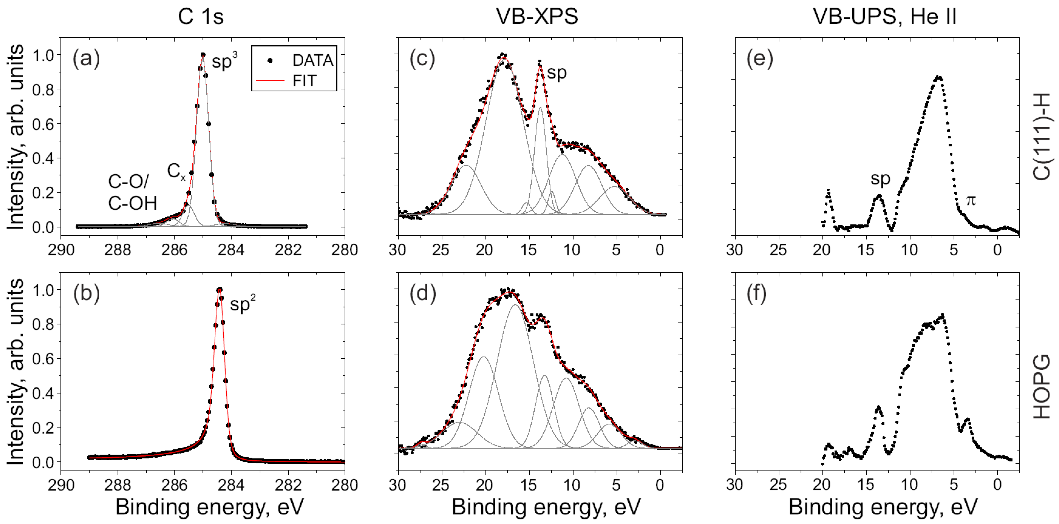
Abstract
:1. Introduction
2. Experimental Details
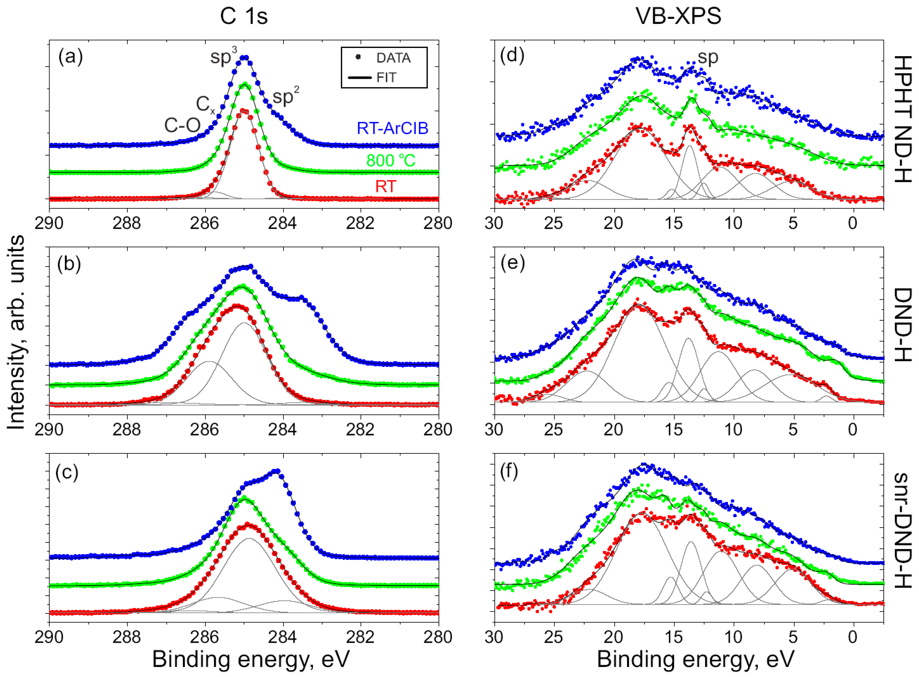
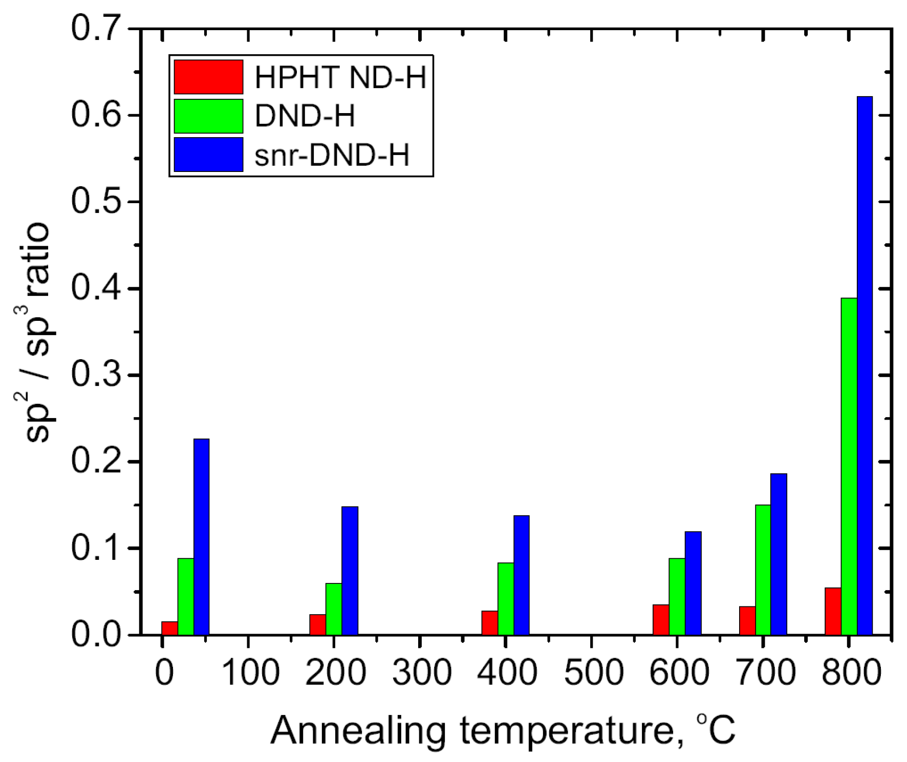
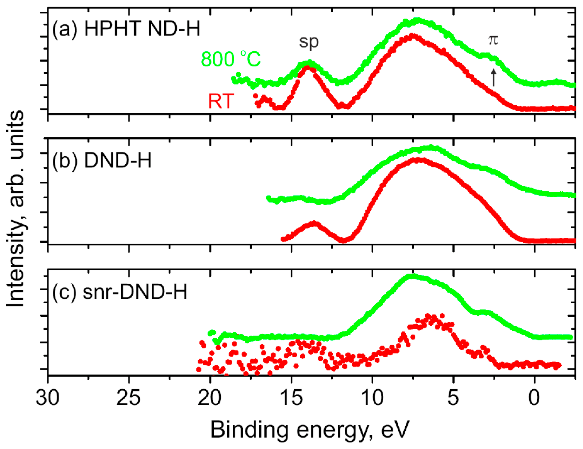
3. Results and Discussion
4. Conclusions
Supplementary Materials
Author Contributions
Funding
Data Availability Statement
Conflicts of Interest
References
- Zhu, D.; Zhang, L.; Ruther, R.E.; Hamers, R.J. Photo-illuminated diamond as a solid-state source of solvated electrons in water for nitrogen reduction. Nat. Mater. 2013, 12, 836–841. [Google Scholar] [CrossRef]
- Marchal, C.; Saoudi, L.; Girard, H.A.; Keller, V.; Arnault, J. Oxidized Detonation Nanodiamonds Act as an Efficient Metal-Free Photocatalyst to Produce Hydrogen Under Solar Irradiation. Adv. Energy Sustain. Res. 2023, 5, 2300260. [Google Scholar] [CrossRef]
- Zhou, Y.; Zhao, K.; Zhang, J.; Zhu, Y.; Ma, Y.; Zhang, H.; Song, D.; Shi, X.; Zhang, L.; Ding, Y. Synergistic effects of nanodiamond modified separators toward highly stable and safe lithium metal batteries. J. Mater. Chem. A 2021, 9, 16046–16055. [Google Scholar] [CrossRef]
- Miliaieva, D.; Djoumessi, A.S.; Čermák, J.; Kolářová, K.; Schaal, M.; Otto, F.; Shagieva, E.; Romanyuk, O.; Pangrác, J.; Kuliček, J.; et al. Absolute energy levels in nanodiamonds of different origins and surface chemistries. Nanoscale Adv. 2023, 5, 4402–4414. [Google Scholar] [CrossRef]
- Afandi, A.; Howkins, A.; Boyd, I.W.; Jackman, R.B. Nanodiamonds for device applications: An investigation of the properties of boron-doped detonation nanodiamonds. Sci. Rep. 2018, 8, 3270. [Google Scholar] [CrossRef]
- Qin, J.-X.; Yang, X.-G.; Lv, C.-F.; Li, Y.-Z.; Liu, K.-K.; Zang, J.-H.; Yang, X.; Dong, L.; Shan, C.-X. Nanodiamonds: Synthesis, properties, and applications in nanomedicine. Mater. Des. 2021, 210, 110091. [Google Scholar] [CrossRef]
- Turner, S.; Shenderova, O.; Da Pieve, F.; Lu, Y.; Yücelen, E.; Verbeeck, J.; Lamoen, D.; Van Tendeloo, G. Aberration-corrected microscopy and spectroscopy analysis of pristine, nitrogen containing detonation nanodiamond: Microscopy and spectroscopy analysis of pristine, nitrogen containing DND. Phys. Status Solidi A 2013, 210, 1976–1984. [Google Scholar] [CrossRef]
- Shenderova, O.; Nunn, N. Production and purification of nanodiamonds. In Nanodiamonds; Elsevier: Amsterdam, The Netherlands, 2017; pp. 25–56. [Google Scholar] [CrossRef]
- Stehlik, S.; Mermoux, M.; Schummer, B.; Vanek, O.; Kolarova, K.; Stenclova, P.; Vlk, A.; Ledinsky, M.; Pfeifer, R.; Romanyuk, O.; et al. Size Effects on Surface Chemistry and Raman Spectra of Sub-5 nm Oxidized High-Pressure High-Temperature and Detonation Nanodiamonds. J. Phys. Chem. C 2021, 125, 5647–5669. [Google Scholar] [CrossRef]
- Arnault, J.C.; Girard, H.A. Hydrogenated nanodiamonds: Synthesis and surface properties. Curr. Opin. Solid State Mater. Sci. 2017, 21, 10–16. [Google Scholar] [CrossRef]
- Maier, F.; Ristein, J.; Ley, L. Electron. affinity of plasma-hydrogenated and chemically oxidized diamond (100) surfaces. Phys. Rev. B 2001, 64, 165411. [Google Scholar] [CrossRef]
- Dideikin, A.T.; Aleksenskii, A.E.; Baidakova, M.V.; Brunkov, P.N.; Brzhezinskaya, M.; Davydov, V.Y.; Levitskii, V.S.; Kidalov, S.V.; Kukushkina, Y.A.; Kirilenko, D.A.; et al. Rehybridization of carbon on facets of detonation diamond nanocrystals and forming hydrosols of individual particles. Carbon 2017, 122, 737–745. [Google Scholar] [CrossRef]
- Arnault, J.C. X-ray Photoemission Spectroscopy applied to nanodiamonds: From surface chemistry to in situ reactivity. Diam. Relat. Mater. 2018, 84, 157–168. [Google Scholar] [CrossRef]
- Yeganeh, M.; Coxon, P.R.; Brieva, A.C.; Dhanak, V.R.; Šiller, L.; Butenko, Y.V. Atomic hydrogen treatment of nanodiamond powder studied with photoemission spectroscopy. Phys. Rev. B 2007, 75, 155404. [Google Scholar] [CrossRef]
- Saoudi, L.; Girard, H.A.; Larquet, E.; Mermoux, M.; Leroy, J.; Arnault, J.-C. Colloidal stability over months of highly crystalline high-pressure high-temperature hydrogenated nanodiamonds in water. Carbon 2023, 202, 438–449. [Google Scholar] [CrossRef]
- Kono, S.; Kageura, T.; Hayashi, Y.; Ri, S.-G.; Teraji, T.; Takeuchi, D.; Ogura, M.; Kodama, H.; Sawabe, A.; Inaba, M.; et al. Carbon 1s X-ray photoelectron spectra of realistic samples of hydrogen-terminated and oxygen-terminated CVD diamond (111) and (001). Diam. Relat. Mater. 2019, 93, 105–130. [Google Scholar] [CrossRef]
- Baer, D.R.; Artyushkova, K.; Cohen, H.; Easton, C.D.; Engelhard, M.; Gengenbach, T.R.; Greczynski, G.; Mack, P.; Morgan, D.J.; Roberts, A. XPS guide: Charge neutralization and binding energy referencing for insulating samples. J. Vac. Sci. Technol. A Vac. Surf. Film. 2020, 38, 031204. [Google Scholar] [CrossRef]
- Kozak, H.; Artemenko, A.; Čermák, J.; Švrček, V.; Kromka, A.; Rezek, B. Oxidation and reduction of nanodiamond particles in colloidal solutions by laser irradiation or radio-frequency plasma treatment. Vib. Spectrosc. 2016, 83, 108–114. [Google Scholar] [CrossRef]
- Romanyuk, O.; Zemek, J.; Houdková, J.; Babčenko, O.; Shagieva, E.; Beranová, K.; Kromka, A.; Jiříček, P. Effects of monoatomic and cluster bombardment with Ar ion beam on the surface of hydrogenated nanocrystalline diamond. Diam. Relat. Mater. 2023, 133, 109748. [Google Scholar] [CrossRef]
- Cuenca, J.A.; Thomas, E.L.H.; Mandal, S.; Morgan, D.J.; Lloret, F.; Araujo, D.; Williams, O.A.; Porch, A. Microwave Permittivity of Trace sp2 Carbon Impurities in Sub-Micron Diamond Powders. ACS Omega 2018, 3, 2183–2192. [Google Scholar] [CrossRef]
- Fujimoto, A.; Yamada, Y.; Koinuma, M.; Sato, S. Origins of sp3C peaks in C 1s X-ray Photoelectron Spectra of Carbon Materials. Anal. Chem. 2016, 88, 6110–6114. [Google Scholar] [CrossRef] [PubMed]
- Wang, Z.-Q.; Yang, Y.-G.; Tai, L.; Lau, L.W.-M.; Zhou, D. Mitigating surface charging in XPS using an in-situ sub-nanometer gold coating technique. Mater. Charact. 2023, 196, 112663. [Google Scholar] [CrossRef]
- Filippi, M.; Calliari, L.; Pucella, G.; Verona-Rinati, G. Temperature evolution of the surface region of CVD diamond: An electron spectroscopy study. Surf. Sci. 2004, 573, 225–236. [Google Scholar] [CrossRef]
- Haerle, R.; Riedo, E.; Pasquarello, A.; Baldereschi, A. sp2/sp3 hybridization ratio in amorphous carbon from C 1 s core-level shifts: X-ray photoelectron spectroscopy and first-principles calculation. Phys. Rev. B 2001, 65, 045101. [Google Scholar] [CrossRef]
- Titantah, J.T.; Lamoen, D. sp3/sp2 characterization of carbon materials from first-principles calculations: X-ray photoelectron versus high energy electron energy-loss spectroscopy techniques. Carbon 2005, 43, 1311–1316. [Google Scholar] [CrossRef]
- Kumaragurubaran, S.; Yamada, T.; Shikata, S. Core Level Photoelectron. Spectroscopic Study on Oxidized Phosphorus-Doped (100) Diamond Surfaces after Vacuum Annealing. Jpn. J. Appl. Phys. 2009, 48, 011602. [Google Scholar] [CrossRef]
- Lau, W.M.; Huang, L.J.; Bello, I.; Yiu, Y.M.; Lee, S.-T. Modification of surface band bending of diamond by low energy argon and carbon ion bombardment. J. Appl. Phys. 1994, 75, 3385–3391. [Google Scholar] [CrossRef]
- Ley, L.; Graupner, R.; Cui, J.B.; Ristein, J. Electronic properties of single crystalline diamond surfaces. Carbon 1999, 37, 793–799. [Google Scholar] [CrossRef]
- Petit, T.; Arnault, J.-C.; Girard, H.A.; Sennour, M.; Bergonzo, P. Early stages of surface graphitization on nanodiamond probed by x-ray photoelectron spectroscopy. Phys. Rev. B 2011, 84, 233407. [Google Scholar] [CrossRef]
- Petit, T.; Arnault, J.-C.; Girard, H.A.; Sennour, M.; Kang, T.-Y.; Cheng, C.-L.; Bergonzo, P. Oxygen hole doping of nanodiamond. Nanoscale 2012, 4, 6792–6799. [Google Scholar] [CrossRef]
- Graupner, R.; Maier, F.; Ristein, J.; Ley, L.; Jung, C. High-resolution surface-sensitive C 1 s core-level spectra of clean and hydrogen-terminated diamond (100) and (111) surfaces. Phys. Rev. B 1998, 57, 12397–12409. [Google Scholar] [CrossRef]
- Liu, J.W.; Liao, M.Y.; Imura, M.; Koide, Y. Band offsets of Al2O3 and HfO2 oxides deposited by atomic layer deposition technique on hydrogenated diamond. Appl. Phys. Lett. 2012, 101, 252108. [Google Scholar] [CrossRef]
- Bydzovska, I.; Shagieva, E.; Gordeev, I.; Romanyuk, O.; Nemeckova, Z.; Henych, J.; Ondic, L.; Kromka, A.; Stehlik, S. Laser-Induced Modification of Hydrogenated Detonation Nanodiamonds in Ethanol. Nanomaterials 2021, 11, 2251. [Google Scholar] [CrossRef] [PubMed]
- Ogawa, S.; Yamada, T.; Ishizduka, S.; Yoshigoe, A.; Hasegawa, M.; Teraoka, Y.; Takakuwa, Y. Vacuum Annealing Formation of Graphene on Diamond C(111) Surfaces Studied by Real-Time Photoelectron Spectroscopy. Jpn. J. Appl. Phys. 2012, 51, 11PF02. [Google Scholar] [CrossRef]
- Romanyuk, O.; Varga, M.; Tulic, S.; Izak, T.; Jiricek, P.; Kromka, A.; Skakalova, V.; Rezek, B. Study of Ni-Catalyzed Graphitization Process of Diamond by in Situ X-ray Photoelectron Spectroscopy. J. Phys. Chem. C 2018, 122, 6629–6636. [Google Scholar] [CrossRef] [PubMed]
- Veyan, J.-F.; de Obaldia, E.; Alcantar-Peña, J.J.; Montes-Gutierrez, J.; Arellano-Jimenez, M.J.; Yacaman, M.J.; Auciello, O. Argon atoms insertion in diamond: New insights in the identification of carbon C 1s peak in X-ray photoelectron spectroscopy analysis. Carbon 2018, 134, 29–36. [Google Scholar] [CrossRef]
- Greczynski, G.; Hultman, L. Critical method evaluation refutes the Ar 2p signal of implanted Ar for referencing X-ray photoelectron spectra. Appl. Surf. Sci. 2023, 635, 157598. [Google Scholar] [CrossRef]
- Gaowei, M.; Muller, E.M.; Rumaiz, A.K.; Weiland, C.; Cockayne, E.; Jordan-Sweet, J.; Smedley, J.; Woicik, J.C. Annealing dependence of diamond-metal Schottky barrier heights probed by hard X-ray photoelectron spectroscopy. Appl. Phys. Lett. 2012, 100, 201606. [Google Scholar] [CrossRef]
- Kern, G.; Hafner, J.; Kresse, G. Atomic and electronic structure of diamond (111) surfaces I. Reconstruction and hydrogen-induced de-reconstruction of the one dangling-bond surface. Surf. Sci. 1996, 366, 445–463. [Google Scholar] [CrossRef]
- Wilson, J.I.B.; Walton, J.S.; Beamson, G. Analysis of chemical vapour deposited diamond films by X-ray photoelectron spectroscopy. J. Electron Spectrosc. Relat. Phenom. 2001, 121, 183–201. [Google Scholar] [CrossRef]
- Kozakov, A.T.; Kochur, A.G.; Kumar, N.; Panda, K.; Nikolskii, A.V.; Sidashov, A.V. Determination of sp2 and sp3 phase fractions on the surface of diamond films from C1s, valence band X-ray photoelectron spectra and CKVV X-ray-excited Auger spectra. Appl. Surf. Sci. 2021, 536, 147807. [Google Scholar] [CrossRef]
- Seshan, V.; Murthy, D.H.K.; Castellanos-Gomez, A.; Sachdeva, S.; Ahmad, H.A.; Janssens, S.D.; Janssen, W.; Haenen, K.; van der Zant, H.S.J.; Sudhölter, E.J.R.; et al. Contactless Photoconductance Study on Undoped and Doped Nanocrystalline Diamond Films. ACS Appl. Mater. Interfaces 2014, 6, 11368–11375. [Google Scholar] [CrossRef]
- Speranza, G. Characterization of Carbon Nanostructures by Photoelectron Spectroscopies. Materials 2022, 15, 4434. [Google Scholar] [CrossRef]
- Speranza, G.; Calliari, L.; Laidani, N.; Anderle, M. Semi-quantitative description of C hybridization via s- and p-partial density of states probing: An electron spectroscopy study. Diam. Relat. Mater. 2000, 9, 1856–1861. [Google Scholar] [CrossRef]
- Mikesova, J.; Miliaieva, D.; Stenclova, P.; Kindermann, M.; Vuckova, T.; Madlikova, M.; Fabry, M.; Veverka, V.; Schimer, J.; Krejci, P.; et al. Nanodiamonds as traps for fibroblast growth factors: Parameters influencing the interaction. Carbon 2022, 195, 372–386. [Google Scholar] [CrossRef]
- Stehlik, S.; Henych, J.; Stenclova, P.; Kral, R.; Zemenova, P.; Pangrac, J.; Vanek, O.; Kromka, A.; Rezek, B. Size and nitrogen inhomogeneity in detonation and laser synthesized primary nanodiamond particles revealed via salt-assisted deaggregation. Carbon 2021, 171, 230–239. [Google Scholar] [CrossRef]
- KolXPD. Software for Spectroscopy Data Measurement and Processing. Available online: https://www.kolibrik.net/en/solutions-products/kolxpd (accessed on 23 March 2024).
- Speranza, G.; Laidani, N. Measurement of the relative abundance of sp2 and sp3 hybridised atoms in carbon based materials by XPS: A critical approach. Part I. Diam. Relat. Mater. 2004, 13, 445–450. [Google Scholar] [CrossRef]
- Rabchinskii, M.K.; Saveliev, S.D.; Stolyarova, D.Y.; Brzhezinskaya, M.; Kirilenko, D.A.; Baidakova, M.V.; Ryzhkov, S.A.; Shnitov, V.V.; Sysoev, V.V.; Brunkov, P.N. Modulating nitrogen species via N-doping and post annealing of graphene derivatives: XPS and XAS examination. Carbon 2021, 182, 593–604. [Google Scholar] [CrossRef]
- Ahmed, A.-I.; Mandal, S.; Gines, L.; Williams, O.A.; Cheng, C.-L. Low temperature catalytic reactivity of nanodiamond in molecular hydrogen. Carbon 2016, 110, 438–442. [Google Scholar] [CrossRef]
- Kondo, T.; Neitzel, I.; Mochalin, V.N.; Urai, J.; Yuasa, M.; Gogotsi, Y. Electrical conductivity of thermally hydrogenated nanodiamond powders. J. Appl. Phys. 2013, 113, 214307. [Google Scholar] [CrossRef]
- Kolarova, K.; Bydzovska, I.; Romanyuk, O.; Shagieva, E.; Ukraintsev, E.; Kromka, A.; Rezek, B.; Stehlik, S. Hydrogenation of HPHT nanodiamonds and their nanoscale interaction with chitosan. Diam. Relat. Mater. 2023, 134, 109754. [Google Scholar] [CrossRef]
- Mermoux, M.; Chang, S.; Girard, H.A.; Arnault, J.-C. Raman spectroscopy study of detonation nanodiamond. Diam. Relat. Mater. 2018, 87, 248–260. [Google Scholar] [CrossRef]
- Sorkin, A.; Tay, B.; Su, H. Three-Stage Transformation Pathway from Nanodiamonds to Fullerenes. J. Phys. Chem. A 2011, 115, 8327–8334. [Google Scholar] [CrossRef] [PubMed]
- Raty, J.-Y.; Galli, G.; Bostedt, C.; Van Buuren, T.; Terminello, L. Quantum Confinement and Fullerenelike Surface Reconstructions in Nanodiamonds. Phys. Rev. Lett. 2003, 90, 037401. [Google Scholar] [CrossRef] [PubMed]
- Dhanak, V.R.; Butenko, Y.V.; Brieva, A.C.; Coxon, P.R.; Alves, L.; Šiller, L. Chemical Functionalization of Nanodiamond by Amino Groups: An X-Ray Photoelectron Spectroscopy Study. J. Nanosci. Nanotech. 2012, 12, 3084–3090. [Google Scholar] [CrossRef]
- Moulder, J.F.; Chastain, J. (Eds.) Handbook of X-ray Photoelectron Spectroscopy: A Reference Book of Standard Spectra for Identification and Interpretation of XPS Data, Update; Perkin-Elmer Corporation: Eden Prairie, MN, USA, 1992. [Google Scholar]
- Ducrozet, F.; Girard, H.A.; Jianu, T.; Peulon, S.; Brun, E.; Sicard-Roselli, C.; Arnault, J.-C. Unintentional formation of nitrate and nitrite ions during nanodiamonds sonication: A source of radical and electron scavengers. Colloids Surf. A Physicochem. Eng. Asp. 2023, 663, 131087. [Google Scholar] [CrossRef]


Disclaimer/Publisher’s Note: The statements, opinions and data contained in all publications are solely those of the individual author(s) and contributor(s) and not of MDPI and/or the editor(s). MDPI and/or the editor(s) disclaim responsibility for any injury to people or property resulting from any ideas, methods, instructions or products referred to in the content. |
© 2024 by the authors. Licensee MDPI, Basel, Switzerland. This article is an open access article distributed under the terms and conditions of the Creative Commons Attribution (CC BY) license (https://creativecommons.org/licenses/by/4.0/).
Share and Cite
Romanyuk, O.; Stehlík, Š.; Zemek, J.; Aubrechtová Dragounová, K.; Kromka, A. Utilizing Constant Energy Difference between sp-Peak and C 1s Core Level in Photoelectron Spectra for Unambiguous Identification and Quantification of Diamond Phase in Nanodiamonds. Nanomaterials 2024, 14, 590. https://0-doi-org.brum.beds.ac.uk/10.3390/nano14070590
Romanyuk O, Stehlík Š, Zemek J, Aubrechtová Dragounová K, Kromka A. Utilizing Constant Energy Difference between sp-Peak and C 1s Core Level in Photoelectron Spectra for Unambiguous Identification and Quantification of Diamond Phase in Nanodiamonds. Nanomaterials. 2024; 14(7):590. https://0-doi-org.brum.beds.ac.uk/10.3390/nano14070590
Chicago/Turabian StyleRomanyuk, Oleksandr, Štěpán Stehlík, Josef Zemek, Kateřina Aubrechtová Dragounová, and Alexander Kromka. 2024. "Utilizing Constant Energy Difference between sp-Peak and C 1s Core Level in Photoelectron Spectra for Unambiguous Identification and Quantification of Diamond Phase in Nanodiamonds" Nanomaterials 14, no. 7: 590. https://0-doi-org.brum.beds.ac.uk/10.3390/nano14070590