Influences of Ga Doping on Crystal Structure and Polarimetric Pattern of SHG in ZnO Nanofilms

Abstract
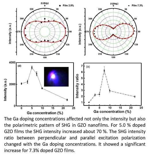
:
1. Introduction
2. Materials and Methods
3. Results and Discussion
4. Conclusions
Author Contributions
Funding
Conflicts of Interest
References
- Chen, M.; Hu, L.F.; Xu, J.X.; Liao, M.Y.; Wu, L.M.; Fang, X.S. ZnO hollow-sphere nanofilm-based high-performance and low-cost photodetec. Small 2011, 7, 2449–2453. [Google Scholar] [PubMed]
- Zhang, C.H.; Wang, G.F.; Liu, M.; Feng, Y.H.; Zhang, Z.D.; Fang, B. A hydroxyllamine electrochemical sensor based on electro deposition of porous ZnO nanofilms onto carbon nanotubes films modified electrode. Electroch. Acta 2010, 55, 2835–2840. [Google Scholar] [CrossRef]
- Wang, J.X.; Zhou, H.J.; Guo, G.Y.; Tan, J.Q.; Wang, Q.J.; Tang, J.; Liu, W.; Shen, H.; Li, J.H.; Zhang, X.L. Enhanced anti-infective efficacy of ZnO nanoreservoirs through a combination of intrinsic anti-biofilm activity and reinforced innate defense. ACS Appl. Mater. Inter. 2017, 9, 33609–33623. [Google Scholar] [CrossRef] [PubMed]
- Park, H.K.; Kang, J.W.; Na, S.I.; Kim, D.Y.; Kim, H.K. Characteristics of indium-free GZO/Ag/GZO and AZO/Ag/AZO multilayer electrode grown by dual target DC sputtering at room temperature for low-cost organic photovoltaics. Sol. Energy Mater. Sol. Cells 2009, 93, 1994–2002. [Google Scholar] [CrossRef]
- Correia, F.C.; Bundaleski, N.; Teodoro, O.M.N.D.; Correia, M.R.; Rebouta, L.; Mendes, A.; Tavares, C.J. XPS analysis of ZnO:Ga films deposited by magnetron sputtering: Substrate bias effect. Appl. Surf. Sci. 2018, 458, 1043–1049. [Google Scholar] [CrossRef]
- Liu, W.S.; Hsieh, W.T.; Chen, S.Y.; Huang, C.S. Improvement of CIGS solar cells with high performance transparent conducting Ti-doped GaZnO thin films. Sol. Energy 2018, 174, 83–96. [Google Scholar] [CrossRef]
- Long, H.; Bao, L.J.; Habeeb, A.A.; Lu, P.X. Effects of doping concentration on the surface plasmonic resonances and optical nonlinearities in AGZO nanotriangle arrays. Opt. Quant. Electron. 2017, 49, 345. [Google Scholar] [CrossRef]
- Stijn, V.C.; Zachary, J.S.; Olivier, D.; Carmen, B.; Sebastian, W.H.; Thierry, V.; Monique, A.V. Morphology and structure of ZIF-8 during crystallisation measured by dynamic angle resolved second harmonic scattering. Nat. Commun. 2018, 9, 3418. [Google Scholar]
- Stefan, K.; Hannu, H.; Thierry, V.; Koen, C. Role of donor and acceptor substituents on the nonlinear optical properties of gold nanoclusters. J. Phys. Chem. C 2018, 122, 4019–4028. [Google Scholar]
- Morales-Saavedra, O.G.; Castaneda, L. Second harmonic generation of fluorine-doped zinc oxide thin films grown on soda-lime glass substrates by a chemical spray technique. Opt. Commun. 2007, 269, 370–377. [Google Scholar] [CrossRef]
- Li, X.H.; Liu, W.W.; Song, Y.L.; Zhang, C.; Long, H.; Wang, K.; Wang, B.; Lu, P.X. Enhancement of the second harmonic generation from WS2 monolayers by cooperating with dielectric microspheres. Adv. Opt. Mater. 2019, 7, 1801270. [Google Scholar] [CrossRef]
- Li, L.; Lan, P.F.; Zhu, X.S.; Huang, T.F.; Zhang, Q.B.; Manfred, L.; Lu, P.X. Reciprocal-space-trajectory perspective on high-harmonic generation in solids. Phys. Rev. Lett. 2019, 122, 193901. [Google Scholar] [CrossRef] [PubMed]
- Lo, K.Y.; Huang, Y.J.; Huang, J.Y.; Feng, Z.C.; Fenwick, W.E.; Pan, M.; Ferguson, I.T. Reflective second harmonic generation from ZnO thin films: A study on the Zn–O Bonding. Appl. Phys. Lett. 2007, 90, 161904. [Google Scholar] [CrossRef]
- Zhao, D.; Ke, S.L.; Hu, Y.H.; Wang, B.; Lu, P.X. Optical bistability of graphene embedded in parity-time-symmetric photonic lattices. J. Opt. Soc. Am. B 2019, 36, 1731–1737. [Google Scholar] [CrossRef]
- Wickberg, A.; Kieninger, C.; Sürgers, C.; Schlabach, S.; Mu, X.K.; Koos, C.; Wegener, M. Second-harmonic generation from ZnO/Al2O3 nanolaminate optical metamaterials grown by atomic-layer deposition. Adv. Opt. Mater. 2016, 4, 1203–1208. [Google Scholar] [CrossRef]
- Ren, M.L.; Agarwal, R.; Nukala, P.; Liu, W.J.; Agarwal, R. Nanotwin detection and domain polarity determination via optical second harmonic generation polarimetry. Nano Lett. 2016, 16, 4404–4409. [Google Scholar] [CrossRef]
- Wang, Y.F.; Liao, L.M.; Hu, T.; Luo, S.; Wu, L.; Wang, J.; Zhang, Z.; Xie, W.; Sun, L.X.; Kavokin, A.V.; et al. Exciton-Polariton Fano Resonance Driven by Second Harmonic Generation. Phys. Rev. Lett. 2017, 118, 063602. [Google Scholar] [CrossRef] [Green Version]
- Weber, N.; Protte, M.; Walter, F.; Georgi, P.; Zentgraf, T.; Meier, C. Double resonant plasmonic nanoantennas for efficient second harmonic generation in zinc oxide. Phys. Rev. B 2017, 95, 205307. [Google Scholar] [CrossRef]
- Kim, C.J.; Brown, L.; Graham, M.W.; Hovden, R.; Havener, R.W.; McEuen, P.L.; Muller, D.A.; Park, J. Stacking order dependent second harmonic generation and topological defects in h-BN bilayers. Nano Lett. 2013, 13, 5660–5665. [Google Scholar] [CrossRef]
- Li, Y.L.; Rao, Y.; Mak, K.F.; You, Y.; Wang, S.Y.; Dean, C.R.; Heinz, T.F. Probing symmetry properties of few-layer MoS2 and h-BN by optical second-harmonic generation. Nano Lett. 2013, 13, 3329–3333. [Google Scholar] [CrossRef]
- Wei, Y.M.; Yu, Y.; Wang, J.; Liu, L.; Ni, H.Q.; Niu, Z.C.; Li, J.T.; Wang, X.H.; Yu, S.Y. Structural discontinuity induced surface second harmonic generation in single, thin zinc-blende GaAs nanowires. Nanoscale 2017, 9, 16066–16072. [Google Scholar] [CrossRef] [PubMed]
- Hu, H.B.; Wang, K.; Long, H.; Liu, W.W.; Wang, B.; Lu, P.X. Precise determination of the crystallographic orientations in single ZnS nanowires by second-harmonic generation microscopy. Nano Lett. 2015, 15, 3351–3357. [Google Scholar] [CrossRef] [PubMed]
- Tom, H.W.K.; Heinz, T.F.; Shen, Y.R. Second-harmonic reflection from silicon surfaces and its relation to structural symmetry. Phys. Rev. Lett. 1983, 51, 1983–1986. [Google Scholar] [CrossRef]
- Brixius, K.; Beyer, A.; Mette, G.; Güdde, J.; Dürr, M.; Stolz, W.; Volz, K.; Höfer, U. Second-harmonic generation as a probe for structural and electronic properties of buried GaP/Si(0 0 1) interfaces. J. Phys-Condens. Matter 2018, 30, 484001. [Google Scholar] [CrossRef] [PubMed]
- Neeman, L.; Ben-Zvi, R.; Rechav, K.; Popovitz-Biro, R.; Oron, D.; Joselevich, E. Crystallographic mapping of guided nanowires by second harmonic generation polarimetry. Nano Lett. 2017, 17, 842–850. [Google Scholar] [CrossRef] [PubMed]
- Han, X.B.; Wang, K.; Long, H.; Hu, H.B.; Chen, J.W.; Wang, B.; Lu, P.X. Highly sensitive detection of the lattice distortion in single bent ZnO nanowires by second-harmonic generation microscopy. ACS Photonics 2016, 3, 1308–1314. [Google Scholar] [CrossRef]
- Long, H.; Bao, L.J.; Wang, K.; Liu, S.H.; Wang, B. Local-field enhancement of optical nonlinearities in the AGZO nanotriangle array. Opt. Mater. 2016, 60, 571–576. [Google Scholar] [CrossRef]
- Dickson, K.M.; Long, H.; Xing, X.Y.; Njoroge, S.; Wang, K.; Wang, B.; Lu, P.X. Gigahertz acoustic vibrations of Ga-doped ZnO nanoparticle array. Nanotechnology 2019, 30, 305201. [Google Scholar]
- Jassim, N.M.; Wang, K.; Han, X.B.; Long, H.; Wang, B.; Lu, P.X. Plasmon assisted enhanced second-harmonic generation in singlehybrid Au/ZnS nanowires. Opt. Mater. 2017, 64, 257–261. [Google Scholar] [CrossRef]
- Chen, J.W.; Wang, K.; Long, H.; Han, X.B.; Hu, H.B.; Liu, W.W.; Wang, B.; Lu, P.X. Tungsten disulfide–gold nanohole hybrid metasurfaces for nonlinear metalenses in the visible region. Nano Lett. 2018, 18, 1344–1350. [Google Scholar] [CrossRef]
- Perillat-Merceroz, G.; Thierry, R.; Jouneau, P.H.; Ferret, P.; Feuillet, G. Compared growth mechanisms of Zn-polar ZnO nanowires on O-polar ZnO and on sapphire. Nanotechnology 2012, 23, 125702. [Google Scholar] [CrossRef] [PubMed]
- Zhan, J.X.; Dong, H.X.; Sun, S.L.; Ren, X.D.; Liu, J.J.; Chen, Z.H.; Lienau, C.; Zhang, L. Surface-energy-driven growth of ZnO hexagonal microtube optical resonators. Adv. Opt. Mater. 2016, 4, 126–134. [Google Scholar] [CrossRef]
- Huang, M.L.; Yan, Y.; Feng, W.H.; Weng, S.X.; Zheng, Z.Y.; Fu, X.Z.; Liu, P. Controllable tuning various ratios of ZnO Polar facets by crystal seed-assisted growth and their photocatalytic activity. Cryst. Growth Des. 2014, 14, 2179–2186. [Google Scholar] [CrossRef]
- Kishimoto, Y.; Nakagawara, O.; Seto, H.; Koshido, Y.; Yoshinoet, Y. Improvement in moisture durability of ZnO transparent conductive films with Ga heavy doping process. Vacuum 2009, 83, 544–547. [Google Scholar] [CrossRef]
- Shinde, S.D.; Deshmukh, A.V.; Date, S.K.; Sathe, V.G.; Adhi, K.P. Effect of Ga doping on micro/structural, electrical and optical properties of pulsed laser deposited ZnO thin films. Thin Solid Films 2011, 520, 1212–1217. [Google Scholar] [CrossRef]
- Fortunato, E.; Raniero, L.; Silva, L.; Goncalves, A.; Pimentel, A.; Barquinha, P.; A’guas, H.; Pereira, L.; Goncalves, G.; Ferreira, I.; et al. Highly stable transparent and conducting gallium-doped zinc oxide thin films for photovoltaic applications. Sol. Energy Mater. Sol. Cells 2008, 92, 1605–1610. [Google Scholar] [CrossRef]
- Vispute, R.D.; Talyansky, V.; Choopun, S.; Sharma, R.P.; Venkatesan, T.; He, M.; Tang, X.; Halpern, J.B.; Spencer, M.G.; Li, Y.X.; et al. Heteroepitaxy of ZnO on GaN and its implications for fabrication of hybrid optoelectronic devices. Appl. Phys. Lett. 1988, 73, 348. [Google Scholar] [CrossRef]
- Helene, S.; Alain, D.; Manuel, G. Investigation of Ga substitution in ZnO powder and opto-electronic properties. Inorg. Chem. 2010, 49, 6853–6858. [Google Scholar]
- Charles, M.; Cosmas, M.M.; Albert, J. Highly conductive and transparent Ga-doped ZnO thin films deposited by chemical spray pyrolysis. Optik 2016, 127, 8317–8325. [Google Scholar]
- Seyda, H.; Fadil, I.; Ramazan, T.S.; Cem, C.; Mohamed, S.; Abdullah, Y.; Tülay, S. Monitoring the characteristic properties of Ga-doped ZnO by Raman spectroscopy and atomic scale calculations. J. Mol. Struct. 2019, 1180, 505–511. [Google Scholar]
- Yao, I.C.; Lee, D.Y.; Tseng, T.Y.; Lin, P. Fabrication and resistive switching characteristics of high compact Ga-doped ZnO nanorod thin film devices. Nanotechnology 2012, 23, 145201. [Google Scholar] [CrossRef] [PubMed]
- Dhara, S.; Imakita, K.; Mizuhata, M.; Fujii, M. Europium doping induced symmetry deviation and its impact on the second harmonic generation of doped ZnO nanowires. Nanotechnology 2014, 25, 225202. [Google Scholar] [CrossRef] [PubMed]
- Vanpoucke, D.E.P. Comment on ‘Europium doping induced symmetry deviation and its impact on the second harmonic generation of doped ZnO nanowires’. Nanotechnology 2014, 25, 458001. [Google Scholar] [CrossRef] [PubMed]
- Wiff, J.P.; Kinemuchi, Y.; Kaga, H.; Ito, C.; Watari, K. Correlations between thermoelectric properties and effective mass caused by lattice distortion in Al-doped ZnO ceramics. J. Eur. Ceram. Soc. 2009, 29, 1413–1418. [Google Scholar] [CrossRef]
- Kumar, N.; Najmaei, S.; Cui, Q.; Ceballos, F.; Ajayan, P.M.; Lou, J.; Zhao, H. Second harmonic microscopy of monolayer MoS2. Phys. Rev. B 2013, 87, 161403. [Google Scholar] [CrossRef]
- Johnson, J.C.; Yan, H.Q.; Schaller, R.D.; Petersen, P.B.; Yang, P.D.; Saykally, R.J. Near-field imaging of nonlinear optical mixing in single zinc oxide nanowires. Nano Lett. 2002, 2, 279–283. [Google Scholar] [CrossRef]
- Michele, M. Nonlinear optical response of a two-dimensional atomic crystal. Opt. Lett. 2016, 41, 187–190. [Google Scholar]
- Mohammad, M.; Adam, C.; Feruz, G. Nonlinear optical susceptibility of atomically thin WX2 crystals. Opt. Mater. 2019, 88, 30–38. [Google Scholar]
- Maria, C.L.; Marco, C. Second harmonic generation from ZnO films and nanostructures. Appl. Phys. Rev. 2015, 2, 031302. [Google Scholar]
- Bhagavannarayana, G.; Parthiban, S.; Subbiah, M. An interesting correlation between crystalline perfection and second harmonic generation efficiency on KCl- and oxalic acid-doped ADP crystals. Cryst. Growth Des. 2008, 8, 446–451. [Google Scholar] [CrossRef]
- Butet, J.; Bachelier, G.; Russier-Antoine, I.; Jonin, C.; Benichou, E.; Brevet, P.F. Interference between selected dipoles and octupoles in the optical second harmonic generation from spherical gold nanoparticles. Phys. Rev. Lett. 2010, 105, 077401. [Google Scholar] [CrossRef] [PubMed]
- Bachelier, G.; Russier-Antoine, I.; Benichou, E.; Jonin, C.; Brevet, P.F. Multipolar second-harmonic generation in noble metal nanoparticles. J. Opt. Soc. Am. B 2008, 25, 955–959. [Google Scholar] [CrossRef]
- Liu, S.W.; Weerasinghe, J.L.; Liu, J.; Weaver, J.; Chen, C.L.; Donner, W.; Xiao, M. Reflective second harmonic generation near resonance in the epitaxial Al-doped ZnO thin film. Opt. Express 2007, 15, 10666–10671. [Google Scholar] [CrossRef] [PubMed]
- Zhang, X.Q.; Tang, Z.K.; Kawasaki, M.; Ohtomo, A.; Koinuma, H. Second harmonic generation in self-assembled ZnO microcrystallite thin films. Thin Solid Films 2004, 450, 320–323. [Google Scholar] [CrossRef]
- Chan, S.W.; Barille, R.; Nunzi, J.M.; Tam, K.H.; Leung, Y.H.; Chan, W.K.; Djurišić, A.B. Second harmonic generation in zinc oxide nanorods. Appl. Phys. B 2006, 84, 351–355. [Google Scholar] [CrossRef]


| Doping Concentration (at. %) | FWHM | 2θ (Degree) | D (Grain Size) (nm) | c (Å) | a (Å) | c/a |
|---|---|---|---|---|---|---|
| 0.0 | 0.326 | 33.91 | 25.47 | 5.285 | 3.381 | 1.563 |
| 2.9 | 0.197 | 34.02 | 42.17 | 5.273 | 3.370 | 1.564 |
| 5.0 | 0.211 | 34.18 | 39.37 | 5.245 | 3.350 | 1.565 |
| 7.3 | 0.154 | 34.33 | 53.71 | 5.219 | 3.332 | 1.566 |
| 9.9 | 0.253 | 33.81 | 32.78 | 5.296 | 3.383 | 1.565 |
© 2019 by the authors. Licensee MDPI, Basel, Switzerland. This article is an open access article distributed under the terms and conditions of the Creative Commons Attribution (CC BY) license (http://creativecommons.org/licenses/by/4.0/).
Share and Cite
Long, H.; Habeeb, A.A.; Kinyua, D.M.; Wang, K.; Wang, B.; Lu, P. Influences of Ga Doping on Crystal Structure and Polarimetric Pattern of SHG in ZnO Nanofilms. Nanomaterials 2019, 9, 905. https://0-doi-org.brum.beds.ac.uk/10.3390/nano9060905
Long H, Habeeb AA, Kinyua DM, Wang K, Wang B, Lu P. Influences of Ga Doping on Crystal Structure and Polarimetric Pattern of SHG in ZnO Nanofilms. Nanomaterials. 2019; 9(6):905. https://0-doi-org.brum.beds.ac.uk/10.3390/nano9060905
Chicago/Turabian StyleLong, Hua, Ammar Ayesh Habeeb, Dickson Mwenda Kinyua, Kai Wang, Bing Wang, and Peixiang Lu. 2019. "Influences of Ga Doping on Crystal Structure and Polarimetric Pattern of SHG in ZnO Nanofilms" Nanomaterials 9, no. 6: 905. https://0-doi-org.brum.beds.ac.uk/10.3390/nano9060905