ToF-SIMS 3D Analysis of Thin Films Deposited in High Aspect Ratio Structures via Atomic Layer Deposition and Chemical Vapor Deposition

 , and
, and 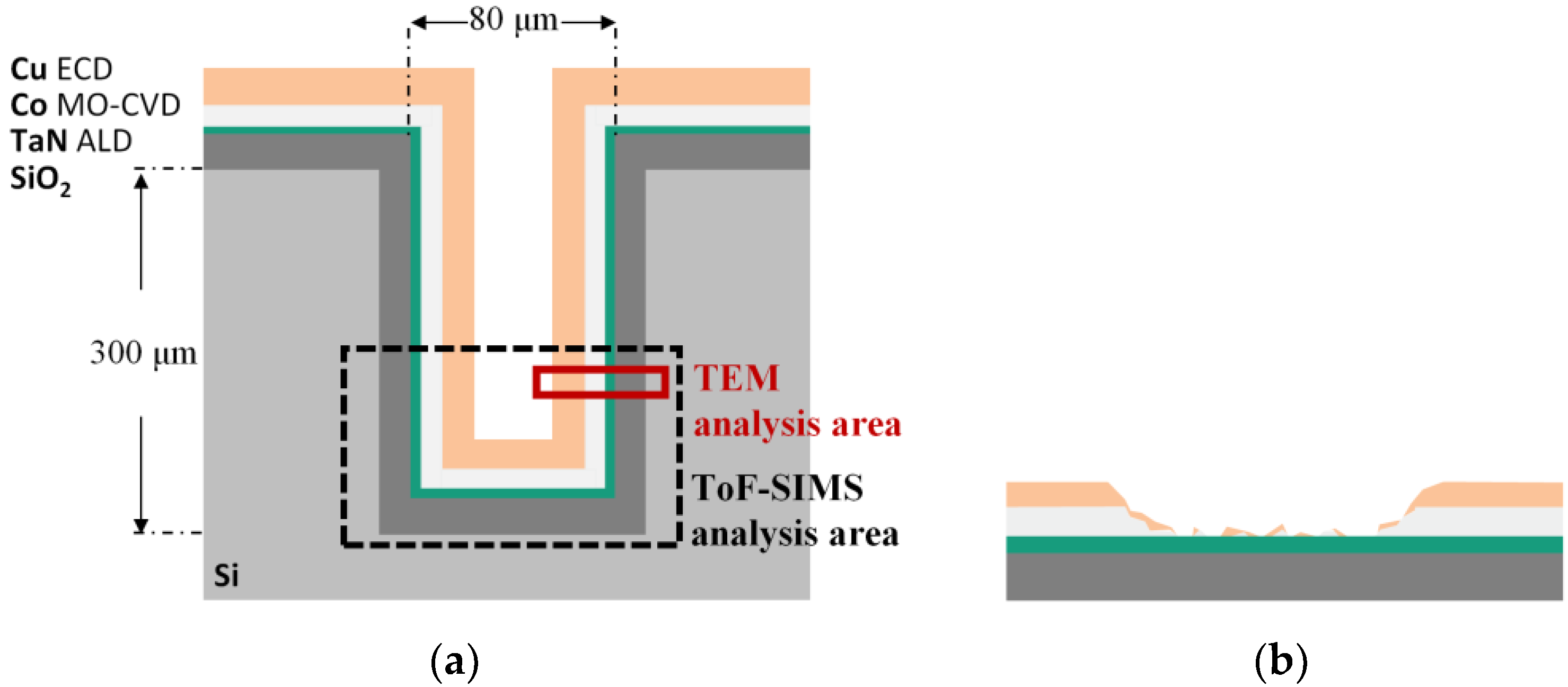
Abstract
:1. Introduction
2. Experimental
2.1. Materials and Thin Films Preparation
2.1.1. TSV Metallization
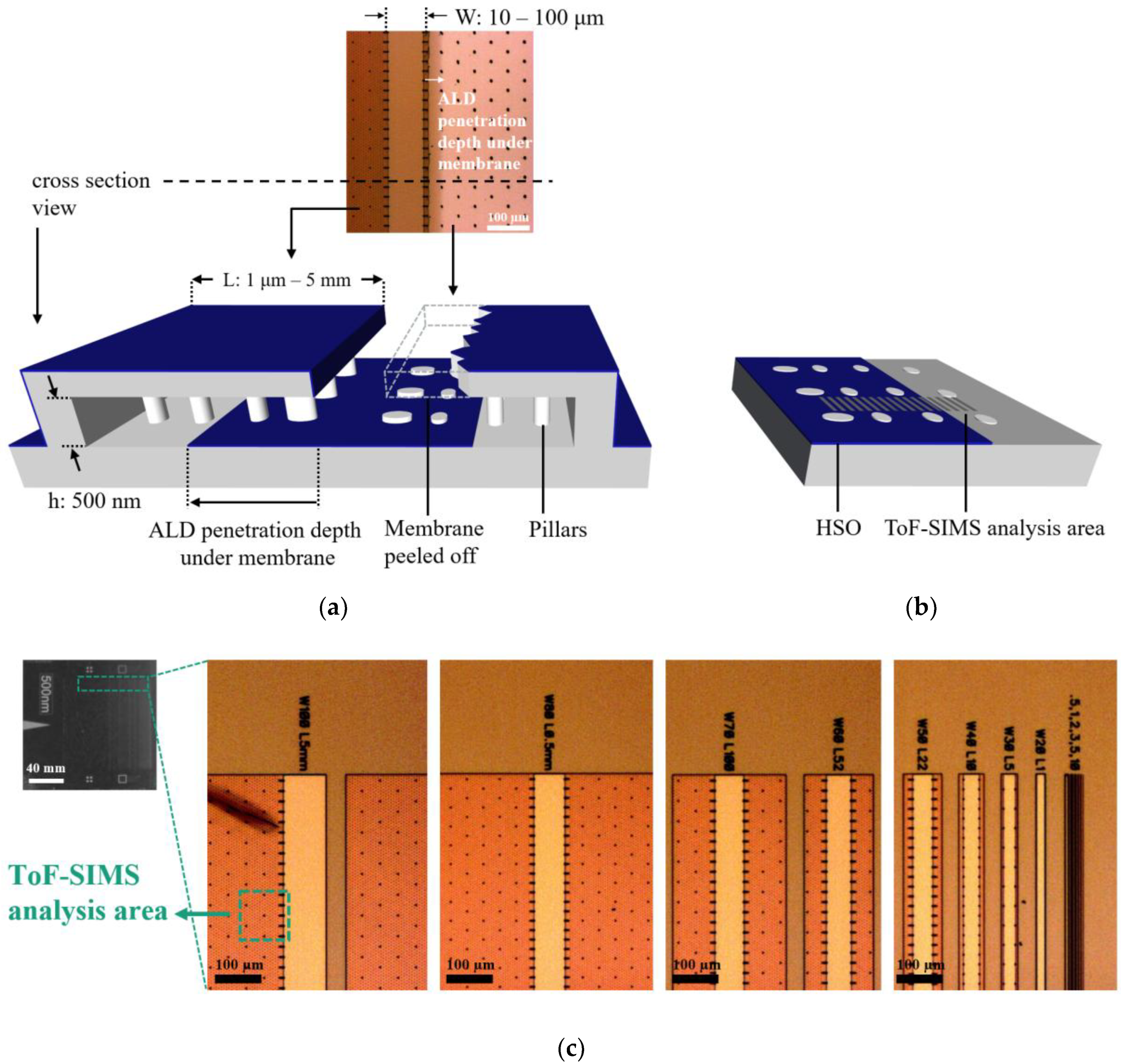
2.1.2. HSO ALD Deposition
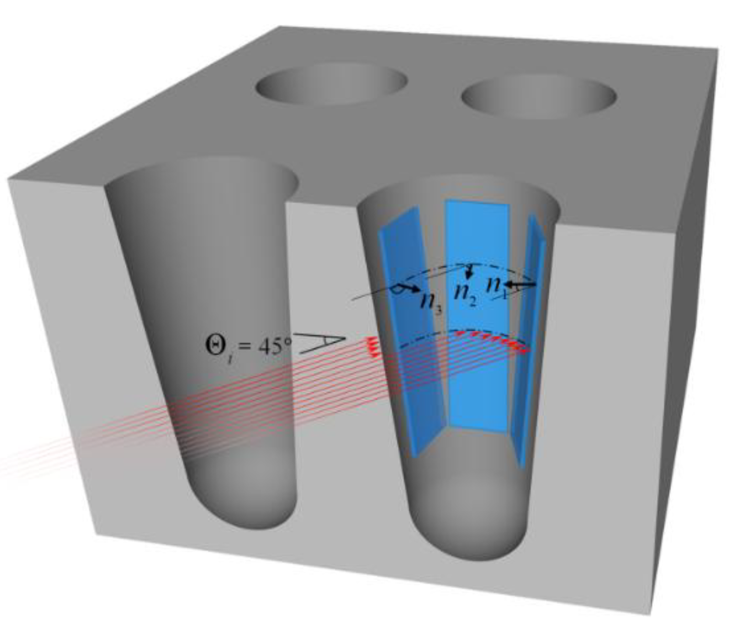
2.2. Analysis Tool Setups
3. Results and Discussion
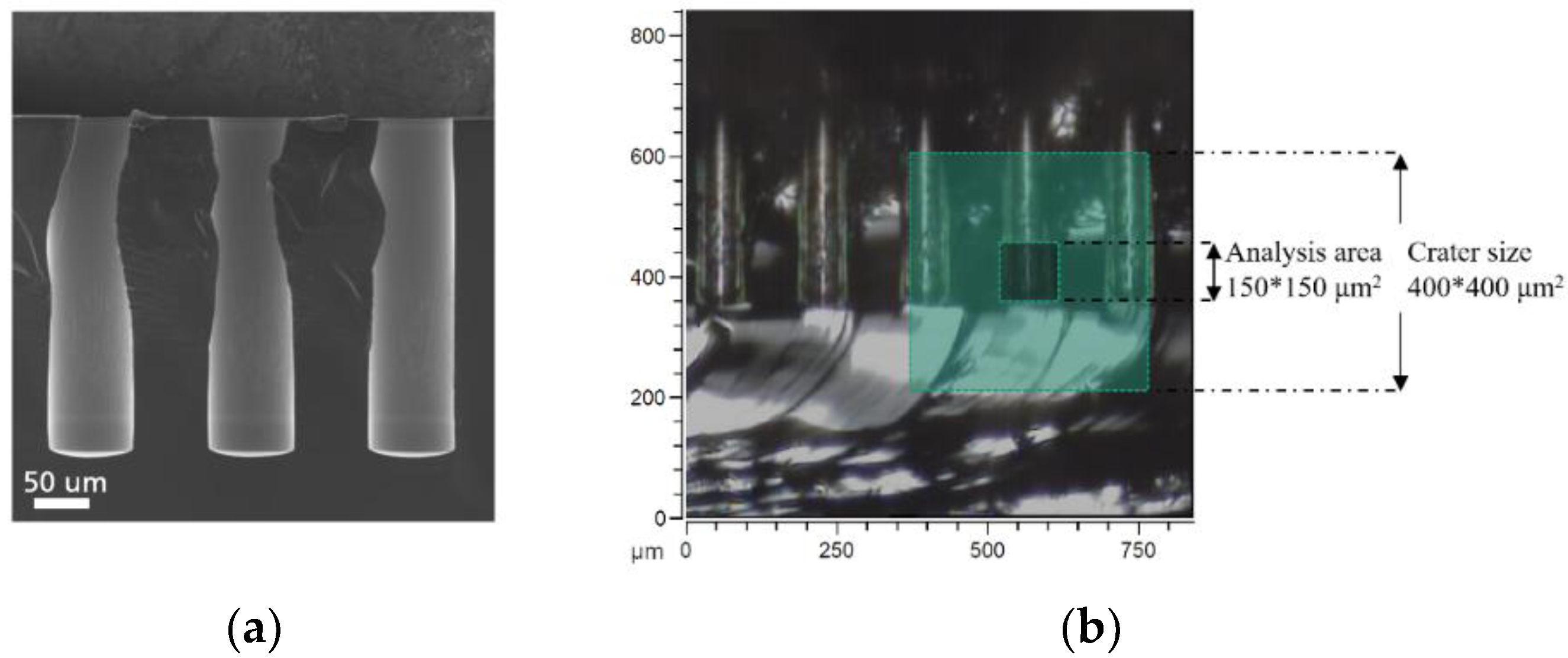
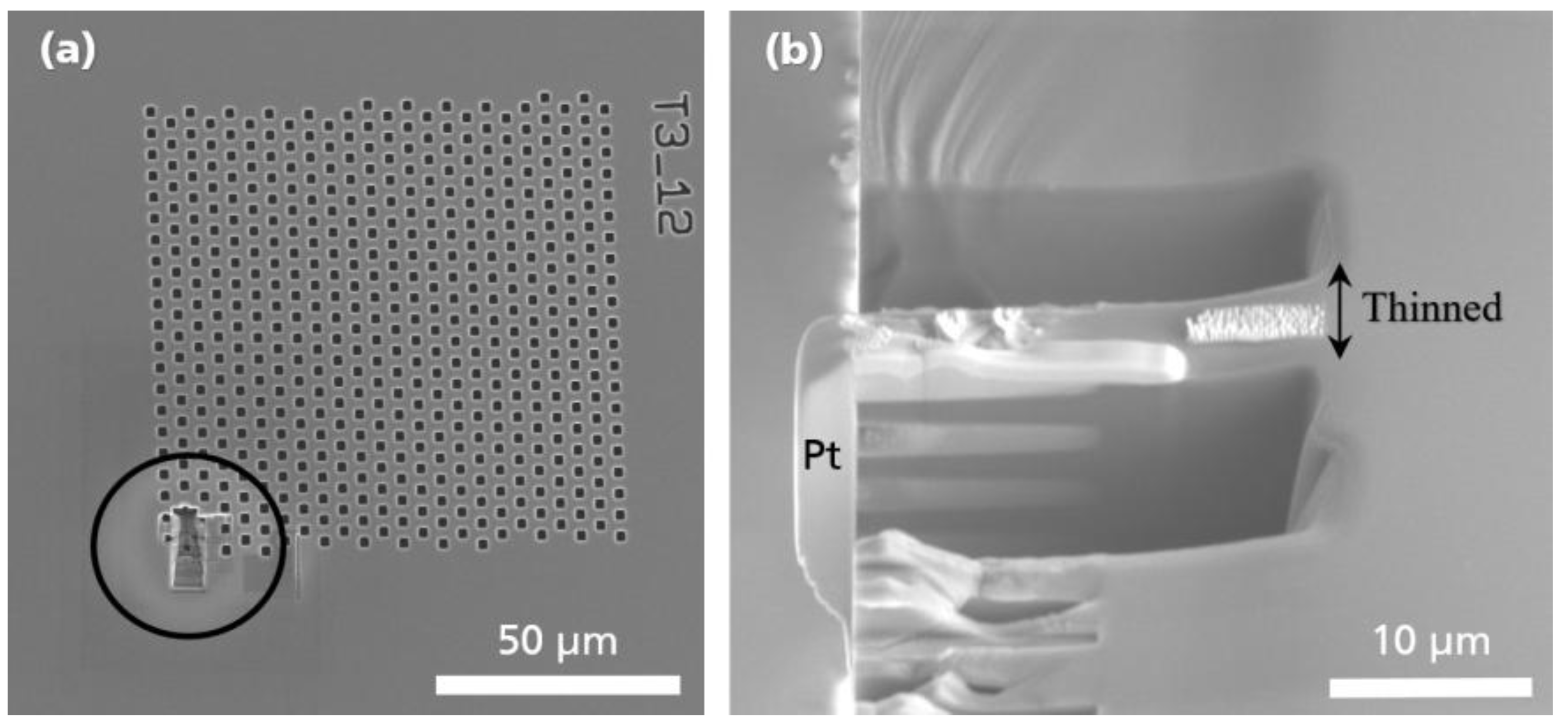
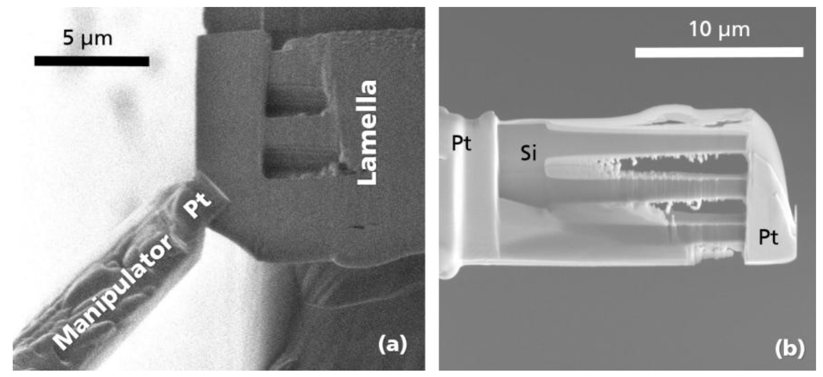
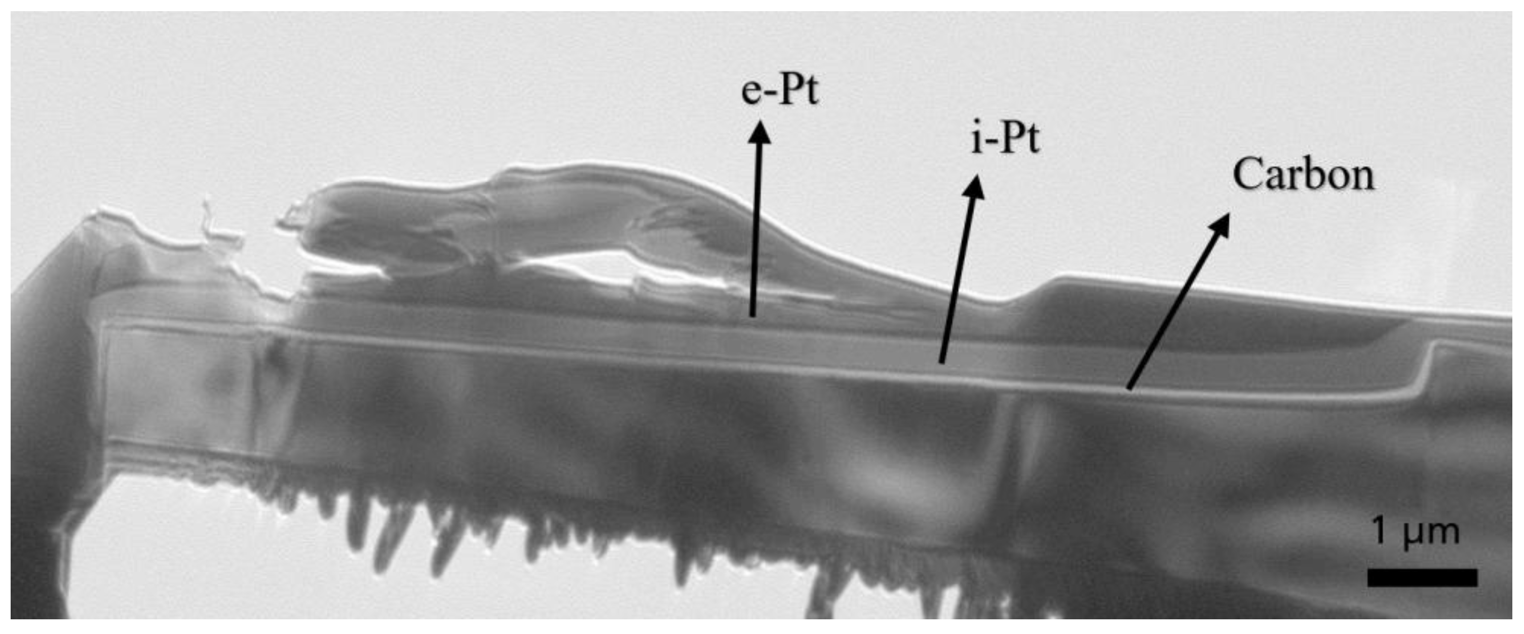
3.1. Vertical High Aspect Ratio Structures
3.2. Lateral High Aspect Ratio Structures
4. Conclusions
Author Contributions
Funding
Acknowledgments
Conflicts of Interest
Appendix A


References
- Riviere, J.C.; Myhra, S. Handbook of Surface and Interface Analysis, 2nd ed.; CRC Press Taylor & Francis Group: Boca Raton, FL, USA, 2017; pp. 65–96. ISBN 978-1-138-11363-3. [Google Scholar]
- Benninghoven, A.; Rüdenauer, F.G.; Werner, H.W. Secondary Ion Mass Spectrometry: Basic Concepts, Instrumental Aspects, Applications, and Trends, 1st ed.; J. Wiley: New York, NY, USA, 1987; p. 435. ISBN 0-471-01056-1. [Google Scholar]
- Hagenhoff, B. High Resolution Surface Analysis by TOF-SIMS. Mikrochim. Acta 2000, 132, 259–271. [Google Scholar]
- Tortora, L.; Urbini, M.; Fabbri, A.; Branchini, P.; Mariucci, L.; Rapisarda, M.; Barra, M.; Chiarella, F.; Cassinese, A.; Di Capua, F.; et al. Three-dimensional characterization of OTFT on modified hydrophobic flexible polymeric substrate by low energy Cs+ ion sputtering. Appl. Surf. Sci. 2018, 448, 628–635. [Google Scholar] [CrossRef]
- Sameshima, J.; Sugahara, T.; Ishina, T.; Nagao, S.; Suganuma, K. 3D imaging of backside metallization of SiC-SBD influenced by annealing. J. Mater. Sci. Mater. Electron. 2019, 30, 10848–10856. [Google Scholar] [CrossRef]
- Siljeström, S. Single Fluid Inclusion Analysis Using ToF-SIMS Implications for Ancient Earth Biodiversity and Paleoenvironment Studies. Ph.D. Thesis, Stockholm University, Stockholm, Sweden, 2011. [Google Scholar]
- Graham, D.J.; Gamble, L.J. Dealing with image shifting in 3D ToF-SIMS depth profiles. Biointerphases 2018, 13, 06E402. [Google Scholar] [CrossRef] [PubMed]
- Oh, H.; Gu, J.M.; Hong, S.J.; May, G.S.; Bakir, M.S. High-aspect ratio through-silicon vias for the integration of microfluidic cooling with 3D microsystems. Microelectron. Eng. 2015, 142, 30–35. [Google Scholar] [CrossRef]
- Taklo, M.M.V.; Klumpp, A.; Ramm, P.; Kwakman, L.; Franz, G.; Taklo, M.M.V. Bonding and TSV in 3D IC Integration: Physical Analysis with a Plasma FIB. Microsc. Microanal. 2011, 25, 9–12. [Google Scholar]
- Armini, S.; El-Mekki, Z.; Vandersmissen, K.; Philipsen, H.; Rodet, S.; Honore, M.; Radisic, A.; Civale, Y.; Beyne, E.; Leunissen, L. Void-Free Filling of HAR TSVs Using a Wet Alkaline Cu Seed on CVD Co as a Replacement for PVD Cu Seed. J. Electrochem. Soc. 2010, 158, H160–H165. [Google Scholar] [CrossRef]
- Esmaeili, S.; Lilienthal, K.; Nagy, N.; Gerlich, L.; Krause, R.; Uhlig, B. Co-MOCVD processed seed layer for through silicon via copper metallization. Microelectron. Eng. 2019, 211, 55–59. [Google Scholar] [CrossRef]
- Müller, J.; Yurchuk, E.; Schlösser, T.; Paul, J.; Hoffmann, R.; Müller, S.; Martin, D.; Slesazeck, S.; Polakowski, P.; Sundqvist, J.; et al. Ferroelectricity in HfO2 enables nonvolatile data storage in 28 nm HKMG. In Proceedings of the 2012 Symposium on VLSI Technology (VLSIT), Honolulu, HI, USA, 12–14 June 2012; pp. 25–26. [Google Scholar] [CrossRef]
- Ali, T.; Polakowski, P.; Riedel, S.; Buttner, T.; Kampfe, T.; Rudolph, M.; Patzold, B.; Seidel, K.; Lohr, D.; Hoffmann, R.; et al. High Endurance Ferroelectric Hafnium Oxide-Based FeFET Memory Without Retention Penalty. IEEE Trans. Electron Devices 2018, 65, 3769–3774. [Google Scholar] [CrossRef]
- Krivokapic, Z.; Rana, U.; Galatage, R.; Razavieh, A.; Aziz, A.; Liu, J.; Shi, J.; Kim, H.J.; Sporer, R.; Serrao, C.; et al. 14nm ferroelectric FinFET technology with steep subthreshold slope for ultra low power applications. In Proceedings of the 2017 IEEE International Electron Devices Meeting (IEDM), San Francisco, CA, USA, 2–6 December 2017; pp. 15.1.1–15.1.4. [Google Scholar] [CrossRef]
- Kobayashi, M.; Hiramoto, T. On device design for steep-slope negative-capacitance field-effect-transistor operating at sub-0.2V supply voltage with ferroelectric HfO2 thin film. AIP Adv. 2016, 6, 025113. [Google Scholar] [CrossRef]
- Kirbach, S.; Kühnel, K.; Weinreich, W. Piezoelectric Hafnium Oxide Thin Films for Energy-Harvesting Applications. In Proceedings of the 2018 IEEE 18th International Conference on Nanotechnology (IEEE-NANO), Cork, Ireland, 23–26 July 2018; pp. 31–34. [Google Scholar] [CrossRef]
- Kühnel, K.; Czernohorsky, M.; Mart, C.; Weinreich, W. High-density energy storage in Si-doped hafnium oxide thin films on area-enhanced substrates. J. Vac. Sci. Technol. B 2019, 37, 021401. [Google Scholar] [CrossRef]
- Mart, C.; Kämpfe, T.; Zybell, S.; Weinreich, W. Layer thickness scaling and wake-up effect of pyroelectric response in Si-doped HfO2. Appl. Phys. Lett. 2018, 112, 052905. [Google Scholar] [CrossRef]
- Anderle, M.; Barozzi, M.; Bersani, M.; Giubertoni, D.; Lazzeri, P. Ultra Shallow Depth Profiling by Secondary Ion Mass Spectrometry Techniques. AIP Conf. Proc. 2003, 695, 695–704. [Google Scholar] [CrossRef]
- Acartürk, T.; Semmelroth, K.; Pensl, G.; Saddow, S.E.; Starke, U. Concentration of N and P in SiC Investigated by Time-Of-Flight Secondary Ion Mass Spectrometry (TOF-SIMS). Mater. Sci. Forum 2009, 483–485, 453–456. [Google Scholar] [CrossRef]
- Gao, F.; Arpiainen, S.; Puurunen, R.L. Microscopic silicon-based lateral high-aspect-ratio structures for thin film conformality analysis. J. Vac. Sci. Technol. A 2014, 33, 010601–010605. [Google Scholar] [CrossRef]
- Ylilammi, M.; Ylivaara, O.M.E.; Puurunen, R.L. Modeling growth kinetics of thin films made by atomic layer deposition in lateral high-aspect-ratio structures. J. Appl. Phys. 2018, 123, 205301. [Google Scholar] [CrossRef] [Green Version]
- Cremers, V.; Puurunen, R.L.; Dendooven, J. Conformality in atomic layer deposition: Current status overview of analysis and modelling. Appl. Phys. Rev. 2019, 6, 21302. [Google Scholar] [CrossRef] [Green Version]
- Puurunen, R.L. Surface chemistry of atomic layer deposition: A case study for the trimethylaluminum / water process. J. Appl. Phys. 2005, 97, 121301. [Google Scholar] [CrossRef]
- Ahern, P. Time-of-Flight Secondary Ion Mass Spectrometry (ToF-SIMS)—Theory and Practice. 2013. Available online: http://www.linkedin.com/in/paulahern1 (accessed on 29 April 2019).
- Kozole, J.; Willingham, D.; Winograd, N. The effect of incident angle on the C60+ bombardment of molecular solids. Appl. Surf. Sci. 2008, 255, 1068–1070. [Google Scholar] [CrossRef] [PubMed]
- Green, F.M.; Gilmore, I.S.; Seah, M.P. TOF-SIMS: Accurate mass scale calibration. J. Am. Soc. Mass Spectrom. 2006, 17, 514–523. [Google Scholar] [CrossRef] [PubMed] [Green Version]
- Lee, J. Time-of-Flight Secondary Ion Mass Spectrometry—Fundamental Issues for Quantitative Measurements and Multivariate Data Analysis. Ph.D. Thesis, Oxford University, Oxford, UK, 2011. [Google Scholar]
- Lee, J.L.S.; Gilmore, I.S.; Seah, M.P.; Fletcher, I.W. Topography and Field Effects in Secondary Ion Mass Spectrometry—Part I: Conducting Samples. J. Am. Soc. Mass Spectrom. 2011, 22, 1718–1728. [Google Scholar] [CrossRef] [PubMed]
- Polakowski, P.; Riedel, S.; Weinreich, W.; Rudolf, M.; Sundqvist, J.; Seidel, K.; Muller, J. Ferroelectric deep trench capacitors based on Al:HfO2 for 3D nonvolatile memory applications. In Proceedings of the 2014 IEEE 6th International Memory Workshop (IMW), Taipei, Taiwan, 18–21 May 2014. [Google Scholar] [CrossRef]
- Mart, C.; Weinreich, W.; Czernohorsky, M.; Riedel, S.; Zybell, S.; Kuhnel, K. CMOS Compatible pyroelectric applications enabled by doped HfO2 films on deep-trench structures. In Proceedings of the 48th European Solid-State Device Research Conference (ESSDERC), Dresden, Germany, 3–6 September 2018; pp. 130–133. [Google Scholar] [CrossRef]
- Richter, C.; Schenk, T.; Park, M.H.; Tscharntke, F.A.; Grimley, E.D.; LeBeau, J.M.; Zhou, C.; Fancher, C.M.; Jones, J.L.; Mikolajick, T.; et al. Si Doped Hafnium Oxide—A ‘Fragile’ Ferroelectric System. Adv. Electron. Mater. 2017, 3, 1700131. [Google Scholar] [CrossRef]
- Ali, T.; Polakowski, P.; Riedel, S.; Büttner, T.; Kämpfe, T.; Rudolph, M.; Pätzold, B.; Seidel, K.; Löhr, D.; Hoffmann, R.; et al. Silicon doped hafnium oxide (HSO) and hafnium zirconium oxide (HZO) based FeFET: A material relation to device physics. Appl. Phys. Lett. 2018, 112, 222903. [Google Scholar] [CrossRef]
- Piehowski, P.D.; Davey, A.M.; Kurczy, M.E.; Sheets, E.D.; Winograd, N.; Ewing, A.G.; Heien, M.L. Time-of-Flight Secondary Ion Mass Spectrometry Imaging of Subcellular Lipid Heterogeneity: Poisson Counting and Spatial Resolution. Anal. Chem. 2009, 81, 5593–5602. [Google Scholar] [CrossRef] [PubMed] [Green Version]
- Vanbellingen, Q.P.; Elie, N.; Eller, M.J.; Della-Negra, S.; Touboul, D.; Brunelle, A. Time-of-flight secondary ion mass spectrometry imaging of biological samples with delayed extraction for high mass and high spatial resolutions. Rapid Commun. Mass Spectrom. 2015, 29, 1187–1195. [Google Scholar] [CrossRef] [PubMed]
- Sodhi, R.N.S. Time-of-flight secondary ion mass spectrometry (TOF-SIMS): - Versatility in chemical and imaging surface analysis. Analyst 2004, 129, 483–487. [Google Scholar] [CrossRef] [PubMed]


© 2019 by the authors. Licensee MDPI, Basel, Switzerland. This article is an open access article distributed under the terms and conditions of the Creative Commons Attribution (CC BY) license (http://creativecommons.org/licenses/by/4.0/).
Share and Cite
Kia, A.M.; Haufe, N.; Esmaeili, S.; Mart, C.; Utriainen, M.; Puurunen, R.L.; Weinreich, W. ToF-SIMS 3D Analysis of Thin Films Deposited in High Aspect Ratio Structures via Atomic Layer Deposition and Chemical Vapor Deposition. Nanomaterials 2019, 9, 1035. https://0-doi-org.brum.beds.ac.uk/10.3390/nano9071035
Kia AM, Haufe N, Esmaeili S, Mart C, Utriainen M, Puurunen RL, Weinreich W. ToF-SIMS 3D Analysis of Thin Films Deposited in High Aspect Ratio Structures via Atomic Layer Deposition and Chemical Vapor Deposition. Nanomaterials. 2019; 9(7):1035. https://0-doi-org.brum.beds.ac.uk/10.3390/nano9071035
Chicago/Turabian StyleKia, Alireza M., Nora Haufe, Sajjad Esmaeili, Clemens Mart, Mikko Utriainen, Riikka L. Puurunen, and Wenke Weinreich. 2019. "ToF-SIMS 3D Analysis of Thin Films Deposited in High Aspect Ratio Structures via Atomic Layer Deposition and Chemical Vapor Deposition" Nanomaterials 9, no. 7: 1035. https://0-doi-org.brum.beds.ac.uk/10.3390/nano9071035