
Multi-Wire Tri-Gate Silicon Nanowires Reaching Milli-pH Unit Resolution in One Micron Square Footprint

 , and
, and 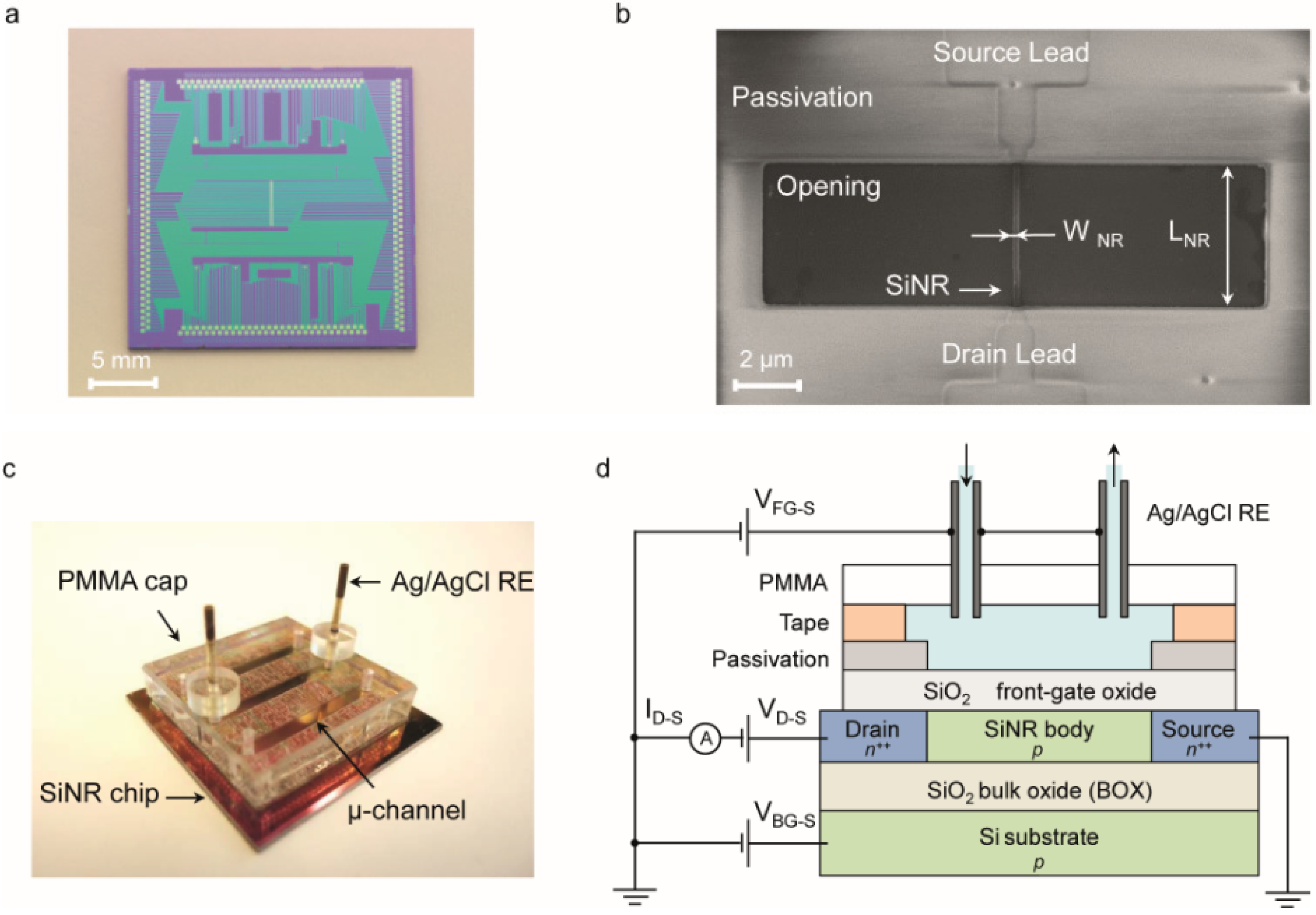
Abstract
:1. Introduction
2. Experimental Section
2.1. Technology and Fabrication Process
2.2. Ag/AgCl Reference Electrode Fabrication
2.3. Microfluidics
2.4. Electrical Characterization
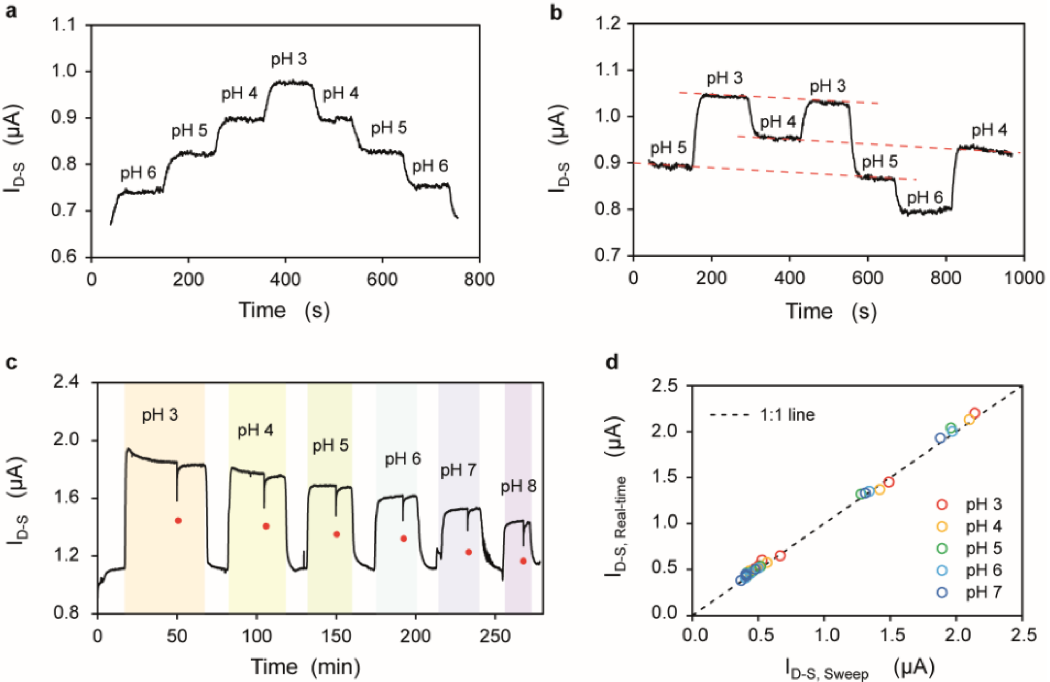
2.5. pH Sensing Experiments
3. Results and Discussion
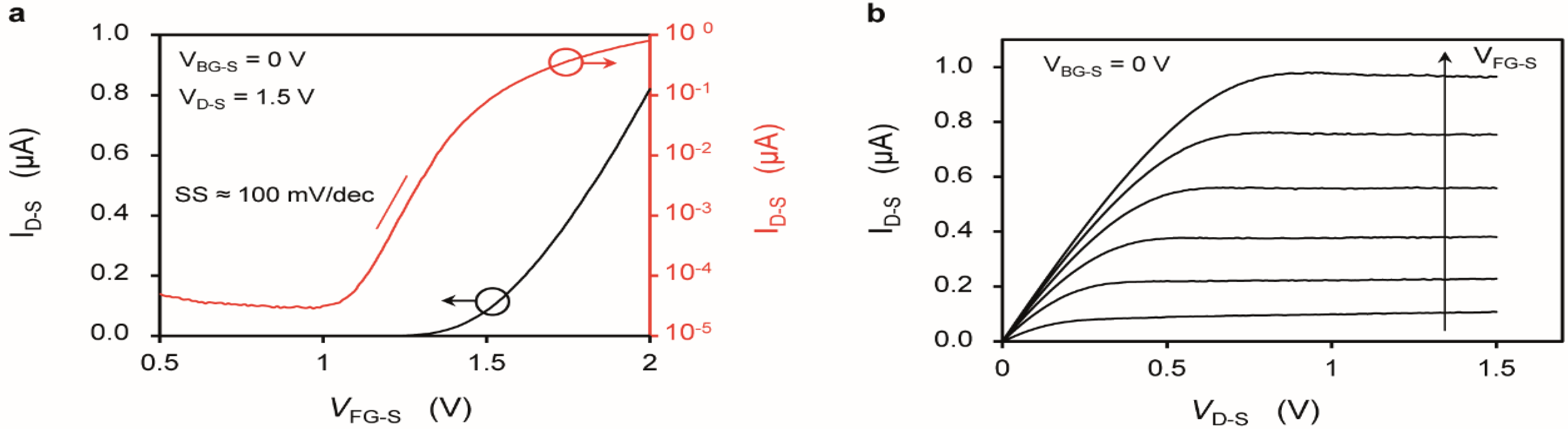
3.1. pH Sensitivity of Single SiNR Devices as a Function of Their Width
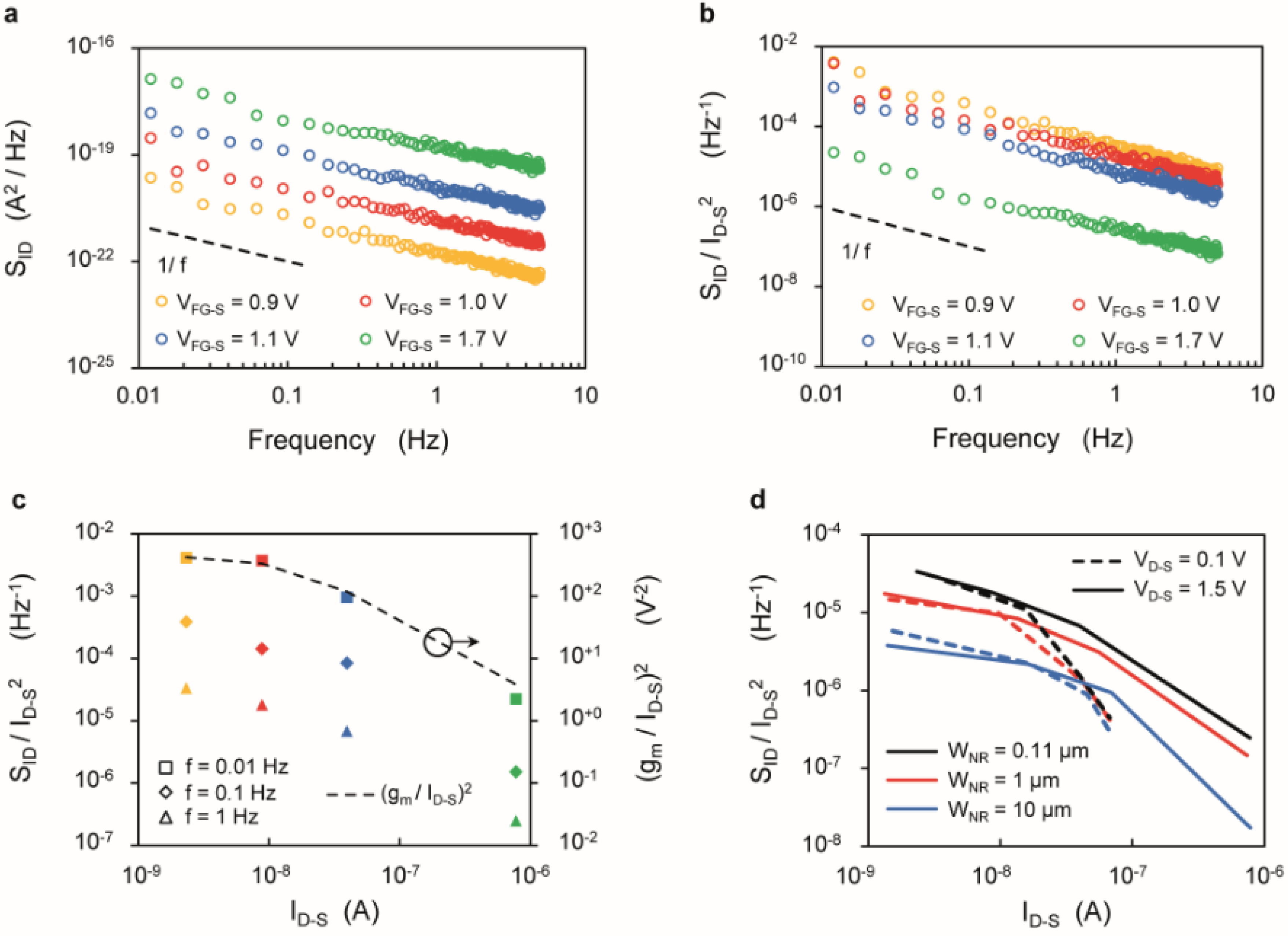
3.2. Noise Characterization of the SiNRs
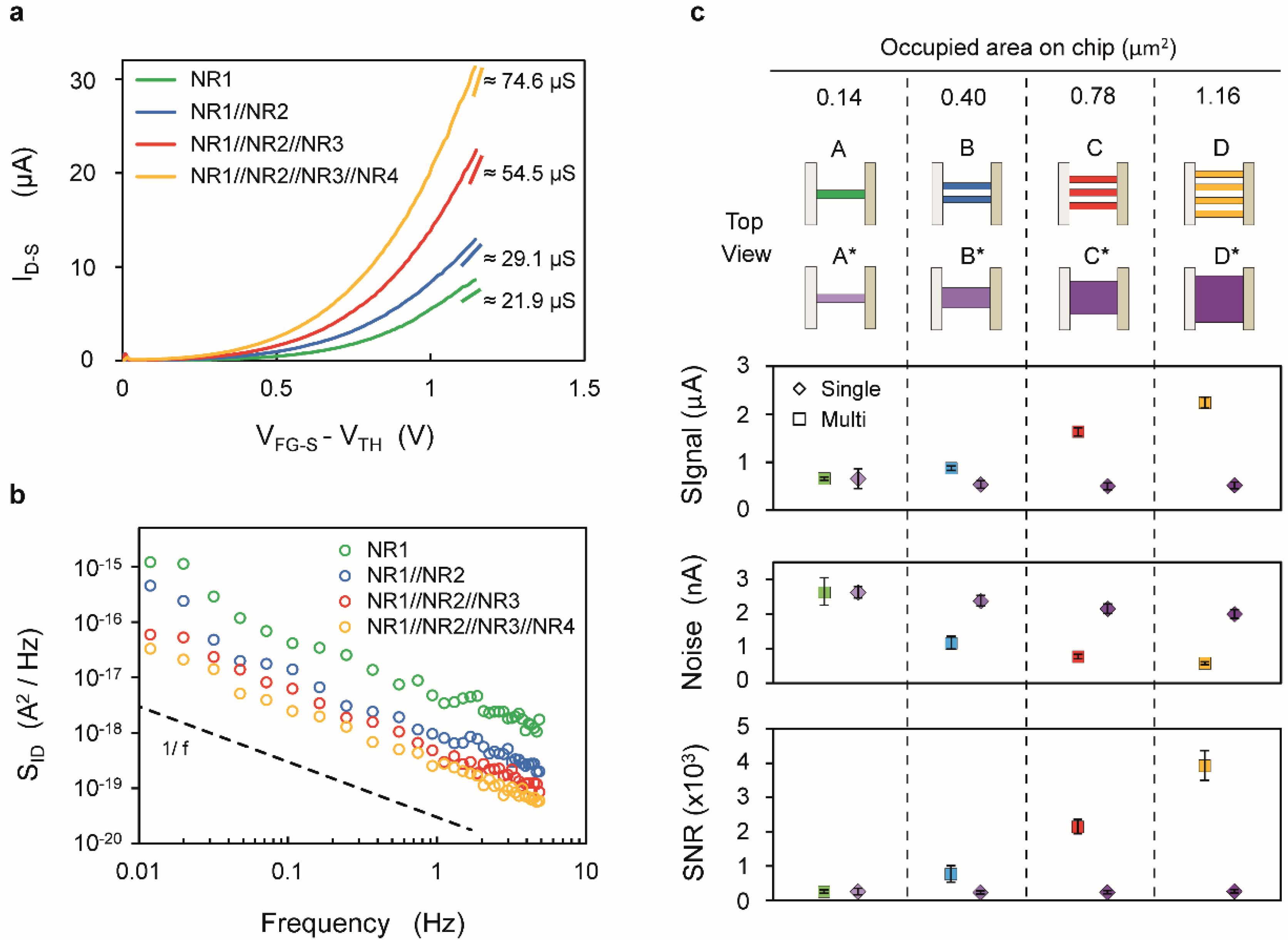
3.3. Multiple-Wire Devices
4. Conclusions
Supplementary Files
Supplementary File 1Acknowledgments
Author Contributions
Conflicts of Interest
References
- James, D. Intel Ivy Bridge unveiled—The first commercial tri-gate, high-k, metal-gate CPU. In Proceedings of the IEEE Custom Integrated Circuits Conference, San Jose, CA, USA, 9–12 September 2012; pp. 1–4.
- Agrawal, N.; Kimura, Y.; Arghavani, R.; Datta, S. Impact of Transistor Architecture (Bulk Planar, Trigate on Bulk, Ultrathin-Body Planar SOI) and Material (Silicon or III-V Semiconductor) on Variation for Logic and SRAM Applications. IEEE Trans. Electron. Devices 2013, 60, 3298–3304. [Google Scholar] [CrossRef]
- Colinge, J.P. FinFETs and Other Multi-Gate Transistors; Springer: New York, NY, USA, 2008. [Google Scholar]
- Sun, X.; Moroz, V.; Damrongplasit, N.; Shin, C.; Liu, T.-J.K. Variation Study of the Planar Ground-Plane Bulk MOSFET, SOI FinFET, and Trigate Bulk MOSFET Designs. IEEE Trans. Electron Devices 2011, 58, 3294–3299. [Google Scholar] [CrossRef]
- Rothberg, J.M.; Hinz, W.; Rearick, T.M.; Schultz, J.; Mileski, W.; Davey, M.; Leamon, J.H.; Johnson, K.; Milgrew, M.J.; Edwards, M.; et al. An integrated semiconductor device enabling non-optical genome sequencing. Nature 2011, 475, 348–352. [Google Scholar] [CrossRef] [PubMed]
- Duarte-Guevara, C.; Lai, F.-L.; Cheng, C.-W.; Reddy, B., Jr.; Salm, E.; Swaminathan, V.; Tsui, Y.-K.; Tuan, H.C.; Kalnitsky, A.; Liu, Y.-S.; et al. Enhanced Biosensing Resolution with Foundry Fabricated Individually Addressable Dual-Gated ISFETs. Anal. Chem. 2014, 86, 8359–8367. [Google Scholar] [CrossRef] [PubMed]
- Guiducci, C.; Spiga, F.M. Another transistor-based revolution: On-chip qPCR. Nat. Methods 2013, 10, 617–618. [Google Scholar] [CrossRef] [PubMed]
- Toumazou, C.; Shepherd, L.M.; Reed, S.C.; Chen, G.I.; Patel, A.; Garner, D.M.; Wang, C.-J.A.; Ou, C.-P.; Amin-Desai, K.; Athanasiou, P.; et al. Simultaneous DNA amplification and detection using a pH-sensing semiconductor system. Nat. Methods 2013, 10, 641–646. [Google Scholar] [CrossRef] [PubMed]
- Bunimovich, Y.L.; Shin, Y.S.; Yeo, W.-S.; Amori, M.; Kwong, G.; Heath, J.R. Quantitative real-time measurements of DNA hybridization with alkylated nonoxidized silicon nanowires in electrolyte solution. J. Anal. Chem. Soc. 2006, 128, 16323–16331. [Google Scholar] [CrossRef] [PubMed]
- Cui, Y.; Wei, Q.Q.; Park, H.K.; Lieber, C.M. Nanowire nanosensors for highly sensitive and selective detection of biological and chemical species. Science 2001, 293, 1289–1292. [Google Scholar] [CrossRef] [PubMed]
- Elfstroem, N.; Karlstroem, A.E.; Linnros, J. Silicon nanoribbons for electrical detection of biomolecules. Nano Lett. 2008, 8, 945–949. [Google Scholar] [CrossRef] [PubMed]
- Gao, X.P.A.; Zheng, G.; Lieber, C.M. Subthreshold Regime has the Optimal Sensitivity for Nanowire FET Biosensors. Nano Lett. 2010, 10, 547–552. [Google Scholar] [CrossRef] [PubMed]
- Gao, Z.; Agarwal, A.; Trigg, A.D.; Singh, N.; Fang, C.; Tung, C.-H.; Fan, Y.; Buddharaju, K.D.; Kong, J. Silicon nanowire arrays for label-free detection of DNA. Anal. Chem. 2007, 79, 3291–3297. [Google Scholar] [CrossRef] [PubMed]
- Hahm, J.; Lieber, C.M. Direct ultrasensitive electrical detection of DNA and DNA sequence variations using nanowire nanosensors. Nano Lett. 2004, 4, 51–54. [Google Scholar] [CrossRef]
- Ishikawa, F.N.; Chang, H.-K.; Curreli, M.; Liao, H.-I.; Olson, C.A.; Chen, P.-C.; Zhang, R.; Roberts, R.W.; Sun, R.; Cote, R.J.; et al. Label-Free, Electrical Detection of the SARS Virus N-Protein with Nanowire Biosensors Utilizing Antibody Mimics as Capture Probes. ACS Nano 2009, 3, 1219–1224. [Google Scholar] [CrossRef] [PubMed]
- Knopfmacher, O.; Tarasov, A.; Fu, W.; Wipf, M.; Niesen, B.; Calame, M.; Schoenenberger, C. Nernst Limit in Dual-Gated Si-Nanowire FET Sensors. Nano Lett. 2010, 10, 2268–2274. [Google Scholar] [CrossRef] [PubMed]
- Li, J.; Zhang, Y.; To, S.; You, L.; Sun, Y. Effect of Nanowire Number, Diameter, and Doping Density on Nano-FET Biosensor Sensitivity. ACS Nano 2011, 5, 6661–6668. [Google Scholar] [CrossRef] [PubMed]
- Li, Z.; Chen, Y.; Li, X.; Kamins, T.I.; Nauka, K.; Williams, R.S. Sequence-specific label-free DNA sensors based on silicon nanowires. Nano Lett. 2004, 4, 245–247. [Google Scholar] [CrossRef]
- Masood, M.N.; Chen, S.; Carlen, E.T.; van den Berg, A. All-(111) Surface Silicon Nanowires: Selective Functionalization for Biosensing Applications. ACS Appl. Mater. Interfaces 2010, 2, 3422–3428. [Google Scholar] [CrossRef] [PubMed]
- Nair, P.R.; Alam, M.A. Design considerations of silicon nanowire biosensors. IEEE Trans. Electron Devices 2007, 54, 3400–3408. [Google Scholar] [CrossRef]
- Patolsky, F.; Zheng, G.F.; Hayden, O.; Lakadamyali, M.; Zhuang, X.W.; Lieber, C.M. Electrical detection of single viruses. Proc. Natl. Acad. Sci. USA 2004, 101, 14017–14022. [Google Scholar] [CrossRef] [PubMed]
- Rajan, N.K.; Duan, X.; Reed, M.A. Performance limitations for nanowire/nanoribbon biosensors. Wiley Interdiscip. Rev. Nanomed. Nanobiotechnol. 2013, 5, 629–645. [Google Scholar] [CrossRef] [PubMed]
- Stern, E.; Klemic, J.F.; Routenberg, D.A.; Wyrembak, P.N.; Turner-Evans, D.B.; Hamilton, A.D.; LaVan, D.A.; Fahmy, T.M.; Reed, M.A. Label-free immunodetection with CMOS-compatible semiconducting nanowires. Nature 2007, 445, 519–522. [Google Scholar] [CrossRef] [PubMed]
- Stern, E.; Vacic, A.; Reed, M.A. Semiconducting Nanowire Field-Effect Transistor Biomolecular Sensors. IEEE Trans. Electron Devices 2008, 55, 3119–3130. [Google Scholar] [CrossRef]
- Tarasov, A.; Fu, W.; Knopfmacher, O.; Brunner, J.; Calame, M.; Schoenenberger, C. Signal-to-noise ratio in dual-gated silicon nanoribbon field-effect sensors. Appl. Phys. Lett. 2011, 98. [Google Scholar] [CrossRef]
- Wang, W.U.; Chen, C.; Lin, K.H.; Fang, Y.; Lieber, C.M. Label-free detection of small-molecule-protein interactions by using nanowire nanosensors. Proc. Natl. Acad. Sci. USA 2005, 102, 3208–3212. [Google Scholar] [CrossRef] [PubMed]
- Zhang, G.-J.; Zhang, L.; Huang, M.J.; Luo, Z.H.H.; Tay, G.K.I.; Lim, E.-J.A.; Kang, T.G.; Chen, Y. Silicon nanowire biosensor for highly sensitive and rapid detection of Dengue virus. Sens. Actuators B Chem. 2010, 146, 138–144. [Google Scholar] [CrossRef]
- Rigante, S.; Scarbolo, P.; Wipf, M.; Stoop, R.L.; Bedner, K.; Buitrago, E.; Bazigos, A.; Bouvet, D.; Calame, M.; Schönenberger, C.; et al. Sensing with Advanced Computing Technology: Fin Field-Effect Transistors with High-k Gate Stack on Bulk Silicon. ACS Nano 2015, 9, 4872–4881. [Google Scholar] [CrossRef] [PubMed]
- Buitrago, E.; Fernández-Bolaños, M.; Rigante, S.; Zilch, C.F.; Schröter, N.S.; Nightingale, A.M.; Ionescu, A.M. The top-down fabrication of a 3D-integrated, fully CMOS-compatible FET biosensor based on vertically stacked SiNWs and FinFETs. Sens. Actuators B Chem. 2014, 193, 400–412. [Google Scholar] [CrossRef]
- Elfstrom, N.; Juhasz, R.; Sychugov, I.; Engfeldt, T.; Karlstrom, A.E.; Linnros, J. Surface charge sensitivity of silicon nanowires: Size dependence. Nano Lett. 2007, 7, 2608–2612. [Google Scholar] [CrossRef] [PubMed]
- Bedner, K.; Guzenko, V.A.; Tarasov, A.; Wipf, M.; Stoop, R.L.; Just, D.; Rigante, S.; Fu, W.; Minamisawa, R.A.; David, C.; et al. pH Response of Silicon Nanowire Sensors: Impact of Nanowire Width and Gate Oxide. Sens. Mater. 2013, 25, 567–576. [Google Scholar]
- Rajan, N.K.; Brower, K.; Duan, X.; Reed, M.A. Limit of detection of field effect transistor biosensors: Effects of surface modification and size dependence. Appl. Phys. Lett. 2014, 104. [Google Scholar] [CrossRef]
- Fritz, J.; Cooper, E.B.; Gaudet, S.; Sorger, P.K.; Manalis, S.R. Electronic detection of DNA by its intrinsic molecular charge. Proc. Natl. Acad. Sci. USA 2002, 99, 14142–14146. [Google Scholar] [CrossRef] [PubMed]
- Gentil, C.; Philippin, G.; Bockelmann, U. Signal enhancement in electronic detection of DNA hybridization. Phys. Rev. E 2007, 75. [Google Scholar] [CrossRef] [PubMed]
- Yao, J.; Yan, H.; Lieber, C.M. A nanoscale combing technique for the large-scale assembly of highly aligned nanowires. Nat. Nanotechnol. 2013, 8, 329–335. [Google Scholar] [CrossRef] [PubMed]
- Halté, C.; Delapierre, G.; Fournier, T.; Buckley, J.; Gely, M.; De Salvo, B.; Baron, T.; Vinet, F. Rapid Top-down Fabrication of Si Nanowire and Fully Automated Test Platform: Application to pH. In Proceedings of the International Conference on Wearable Micro and Nano Technologies for Personalized Health, Valencia, Spain, 21–23 May 2008.
- Accastelli, E.; Cappi, G.; Buckley, J.; Ernst, T.; Guiducci, C. Comparison between front- and back-gating of Silicon Nanoribbons in real-time sensing experiments. In Proceedings of the IEEE Conference on Nanotechnology, Beijing, China, 5–8 August 2013; pp. 517–520.
- Pud, S.; Li, J.; Sibiliev, V.; Petrychuk, M.; Kovalenko, V.; Offenhäusser, A.; Vitusevich, S. Liquid and Back Gate Coupling Effect: Toward Biosensing with Lowest Detection Limit. Nano Lett. 2014, 14, 578–584. [Google Scholar] [CrossRef] [PubMed]
- Bergveld, P.; VanHal, R.; Eijkel, J. The Remarkable Similarity between the Acid-Base Properties of ISFETs and Proteins and the Consequences for the Design of ISFET Biosensors. Biosens. Bioelectron. 1995, 10, 405–414. [Google Scholar] [CrossRef]
- Bousse, L.; Bergveld, P. The role of buried OH sites in the response mechanism of inorganic-gate pH-sensitive ISFETs. Sens. Actuators 1984, 6, 65–78, (no A and B in Sensors and Actuators at that time). [Google Scholar] [CrossRef]
- Yates, D.E.; Levine, S.; Healy, T.W. Site-binding model of the electrical double layer at the oxide/water interface. J. Chem. Soc. Faraday Trans. 1: Phys. Chem. Condens. Phases 1974, 70, 1807–1818. [Google Scholar] [CrossRef]
- Bergveld, P. Thirty years of ISFETOLOGY—What happened in the past 30 years and what may happen in the next 30 years. Sens. Actuators B Chem. 2003, 88, 1–20. [Google Scholar] [CrossRef]
- Siu, W.M.; Cobbold, R. Basic Properties of the Electrolyte-SiO2-Si System—Physical and Theoretical Aspects. IEEE Trans. Electron Devices 1979, 26, 1805–1815. [Google Scholar] [CrossRef]
- Vu, X.T.; GhoshMoulick, R.; Eschermann, J.F.; Stockmann, R.; Offenhaeusser, A.; Ingebrandt, S. Fabrication and application of silicon nanowire transistor arrays for biomolecular detection. Sens. Actuators B Chem. 2010, 144, 354–360. [Google Scholar] [CrossRef]
- Fossum, J.G.; Yang, J.W.; Trivedi, V.P. Suppression of corner effects in triple-gate MOSFETs. IEEE Electron Device Lett. 2003, 24, 745–747. [Google Scholar] [CrossRef]
- Kim, S.; Rim, T.; Kim, K.; Lee, U.; Baek, E.; Lee, H.; Baek, C.-K.; Meyyappan, M.; Deen, M.J.; Lee, J.-S. Silicon nanowire ion sensitive field effect transistor with integrated Ag/AgCl electrode: pH sensing and noise characteristics. Analyst 2011, 136, 5012–5016. [Google Scholar] [CrossRef] [PubMed]
- Zhuge, J.; Wang, R.; Huang, R.; Tian, Y.; Zhang, L.; Kim, D.-W.; Park, D.; Wang, Y. Investigation of Low-Frequency Noise in Silicon Nanowire MOSFETs. IEEE Electron Device Lett. 2009, 30, 57–60. [Google Scholar] [CrossRef]
- Simoen, E.; Claeys, C. On the flicker noise in submicron silicon MOSFETs. Solid State Electron. 1999, 43, 865–882. [Google Scholar] [CrossRef]
- Ghibaudo, G.; Roux, O.; Nguyen-Duc, C.; Balestra, F.; Brini, J. Improved Analysis of Low-Frequency Noise in Field-Effect Mos-Transistors. Phys. Status Solidi A Appl. Res. 1991, 124, 571–581. [Google Scholar] [CrossRef]
- Harris, F.J. On the use of windows for harmonic analysis with the discrete Fourier transform. Proc. IEEE 1978, 66, 51–83. [Google Scholar] [CrossRef]
- Kirchner, J.W. Publisher’s note: Aliasing in 1/f(alpha) noise spectra: Origins, consequences, and remedies. Phys. Rev. E 2005, 71. [Google Scholar] [CrossRef]
- Caloyannides, M.A. Microcycle Spectral Estimates of 1-F Noise in Semiconductors. J. Appl. Phys. 1974, 45, 307–316. [Google Scholar] [CrossRef]
- Foster, S.; Cranch, G.A.; Tikhomirov, A. Experimental evidence for the thermal origin of 1/f frequency noise in erbium-doped fiber lasers. Phys. Rev. A 2009, 79-5, 053802-1–053802-7. [Google Scholar] [CrossRef]
- Kasdin, N.J. Discrete Simulation of Colored Noise and Stochastic-Processes and 1/F(Alpha) Power-Law Noise Generation. Proc. IEEE 1995, 83, 802–827. [Google Scholar] [CrossRef]
- Rajan, N.K.; Routenberg, D.A.; Reed, M.A. Optimal signal-to-noise ratio for silicon nanowire biochemical sensors. Appl. Phys. Lett. 2011, 98, 264107-1–264107-3. [Google Scholar] [CrossRef] [PubMed]
- Clément, N.; Han, X.L.; Larrieu, G. Electronic transport mechanisms in scaled gate-all-around silicon nanowire transistor arrays. Appl. Phys. Lett. 2013, 103, 263504. [Google Scholar] [CrossRef]
- Regonda, S.; Tian, R.; Gao, J.; Greene, S.; Ding, J.; Hu, W. Silicon multi-nanochannel FETs to improve device uniformity/stability and femtomolar detection of insulin in serum. Biosens. Bioelectron. 2013, 45, 245–251. [Google Scholar] [CrossRef] [PubMed]
- Tartagni, M.; Crescentini, M.; Rossi, M.; Morgan, H.; Sangiorgi, E. An AC and phase nanowire sensing for site-binding detection. In Proceedings of the IEEE International Electron Device Meeting, San Francisco, CA, USA, 15–17 December 2014; pp. 31.2.1–31.2.4.


© 2016 by the authors; licensee MDPI, Basel, Switzerland. This article is an open access article distributed under the terms and conditions of the Creative Commons by Attribution (CC-BY) license (http://creativecommons.org/licenses/by/4.0/).
Share and Cite
Accastelli, E.; Scarbolo, P.; Ernst, T.; Palestri, P.; Selmi, L.; Guiducci, C. Multi-Wire Tri-Gate Silicon Nanowires Reaching Milli-pH Unit Resolution in One Micron Square Footprint. Biosensors 2016, 6, 9. https://0-doi-org.brum.beds.ac.uk/10.3390/bios6010009
Accastelli E, Scarbolo P, Ernst T, Palestri P, Selmi L, Guiducci C. Multi-Wire Tri-Gate Silicon Nanowires Reaching Milli-pH Unit Resolution in One Micron Square Footprint. Biosensors. 2016; 6(1):9. https://0-doi-org.brum.beds.ac.uk/10.3390/bios6010009
Chicago/Turabian StyleAccastelli, Enrico, Paolo Scarbolo, Thomas Ernst, Pierpaolo Palestri, Luca Selmi, and Carlotta Guiducci. 2016. "Multi-Wire Tri-Gate Silicon Nanowires Reaching Milli-pH Unit Resolution in One Micron Square Footprint" Biosensors 6, no. 1: 9. https://0-doi-org.brum.beds.ac.uk/10.3390/bios6010009