Trilayer Films of YBa2Cu3O7−x/LaAlO3/YBa2Cu3O7−x with Superconducting Properties Prepared via Sol-Gel Method


1
College of Vanadium and Titanium, Panzhihua University, Panzhihua 617000, China
2
School of Material Science and Engineering, Xi’an University of Technology, Xi’an 710048, China
3
School of Biological and Chemical Engineering, Panzhihua University, Panzhihua 617000, China
*
Author to whom correspondence should be addressed.
Coatings 2020, 10(7), 686; https://0-doi-org.brum.beds.ac.uk/10.3390/coatings10070686
Submission received: 23 June 2020
/
Revised: 12 July 2020
/
Accepted: 15 July 2020
/
Published: 16 July 2020
(This article belongs to the Special Issue Superconducting Films and Nanostructures)
Abstract
:The YBa2Cu3O7−x/LaAlO3/YBa2Cu3O7−x (YBCO/LAO/YBCO) heterogeneous trilayer film structures were prepared on the LaAlO3 (001) single-crystal substrate via the sol-gel method. The characteristics of the phase, orientation, and superconducting properties were studied via an X-ray diffractometer and a comprehensive physical property measurement system. The results show that when the LAO layer was thin (<40 nm), the trilayer films were relatively pure and had a high c-axis orientation. When the nominal thickness of the LAO layer increased to 70 nm, non-c-axis oriented grains started to appear in the trilayer film. In this case, the top and bottom YBCO layers exhibited superconducting properties, and the resistance was found to be zero at 80.1 and 72.5 K, respectively. In addition, for the YBCO/LAO (40 nm)/YBCO structure, the intermediate LAO layer was too thin to completely cover the surface of the underlying YBCO. This resulted in point contact and micro-bridge contact in several micro-regions, thus forming a weak connection and exhibiting a current-voltage (I–V) characteristic similar to the direct-current (DC) Josephson effect. On the other hand, for the YBCO/LAO (70 nm)/YBCO structure, the thicker LAO layer could completely cover the underlying YBCO surface, which could isolate the superconducting current between the YBCO layers.
1. Introduction
YBa2Cu3O7−x (YBCO) films have broad application prospects in the field of superconducting electronics. High-quality single-layer YBCO films can already be used to prepare planar resonators, transmission lines, and filters. The YBCO/dielectric/YBCO sandwich structure is essential in the integration of complex circuits, such as flux transformers, and in the integration of microwave components. Therefore, it is crucial to investigate its preparation technology [1,2,3].
If the intermediate dielectric layer is thin enough (~2 nm), the Josephson effect also occurs. Tsuchiya et al. prepared the a-YBCO/PrGaO3 (~2.0–3.2 nm)/a-YBCO structure using a pulsed laser deposition system and observed the Josephson effect [4]. Later, Moeckly et al. prepared the full c-axis Josephson junction based on the YBCO via an in-situ deposition technology, and found that the IcRn value of the junction reached a maximum of 1.6 mV at 4.2 K, presenting great application potential [5]. Furthermore, it is well known that the critical current density (Jc) of the YBCO film decreases sharply under an applied magnetic field, which increases the noise of the microwave device, ultimately affecting its resolution. Therefore, the quality of the superconducting electronic components also depends on the ability of the film to transmit superconducting current, especially under a magnetic field [6]. It is found that the introduction of nano-scale crystal defects into the YBCO film can play the role of magnetic flux pinning, which can significantly increase the Jc value under a magnetic field [7,8,9,10]. Introducing an appropriate interface in the superconducting film is also an effective method to improve the Jc of the film. Wang and Wu studied the relationship between Jc and the thickness of the YBCO/CeO2/YBCO trilayer film grown via pulsed laser deposition. They found that when the thickness of the YBCO layer was fixed at 250 nm, the Jc of the whole trilayer film was enhanced with increasing the thickness tI of the intermediate insulating layer (from tI = 0 nm to tI = 20 nm) due to the degeneration of the magnetic coupling at the interface [11]. Furthermore, in the multilayer periodic structures of YBCO/CeO2 [12] and YBCO/NdBCO [13], the Jc values are also enhanced.
The LaAlO3 (LAO) crystal has a pseudocubic structure at room temperature with the cell parameter a = 0.379 nm. The lattice mismatch between YBCO (a = 0.382 nm; b = 0.386 nm) and LAO is small and thus LAO is often used as a substrate for epitaxial growth of YBCO films. In addition, the cell parameters of LAO are smaller than those of YBCO in both a and b directions, which causes YBCO to suffer compressive stress in the a—b plane. This circumstance is conducive to improve the superconducting transition temperature (Tc) of the YBCO film [14,15]. Therefore, in order to prepare the YBCO/LAO/YBCO trilayer structure, a modulation of the two key superconducting parameters, Jc and Tc, is expected. However, there are very few studies on this structure, and the preparation methods are based only on vacuum physical deposition [16]. If a chemical solution method, such as the sol-gel method, can be used to prepare the YBCO/LAO/YBCO trilayer heterogeneous structure, two advantages can be envisaged. Not only the stoichiometric ratio of each element can be controlled accurately, but also the mobility of sol can be useful to produce a novel film interface, different from that obtained using the more common vacuum deposition process, thereby demonstrating different superconducting properties.
In our previous work, trilayer structures of YBCO/LAO/YBCO were prepared via the sol-gel method, and their magnetic properties were characterized. It was found that the Jc of the structure could be modulated by changing the thickness of the LAO layer [17]. Here, the electrical properties of the YBCO/LAO/YBCO trilayer structure are further analyzed, focusing on the modulation of the critical temperature Tc and of the critical current Ic by adjusting the thickness of the LAO middle layer.
2. Experiments
2.1. Film Preparation
2.1.1. Preparation of the YBCO Film
The YBCO film was obtained using a low-fluorine sol-gel method [18]. Firstly, yttrium acetate was dissolved in a mixed solution of trifluoroacetic acid and deionized water. After dry vacuum distillation, the generated powder was dissolved in methanol to obtain solution A. Secondly, barium acetate was dissolved in a mixed solution of acrylic acid and methanol to obtain solution B. Thirdly, copper acetate was dissolved in a mixed solution of acrylic acid and methanol to obtain solution C. Finally, solutions A, B, and C were mixed and stirred to obtain a low-fluorine YBCO precursor solution. By adjusting the amount of methanol, the concentration of YBCO sol was fixed at 1.2 mol/L (calculated based on the total moles of metal ions). Using the low-fluorine solution, the YBCO gel films were produced via dip coating on single-crystal LAO (001) substrate. The withdrawal speed was controlled at 1 mm/s for the bottom YBCO and 2 mm/s for the top YBCO. The dip-coated gel films were pyrolyzed at 450 °C for 15 min and then fired at 800 °C for 100 min. The mixture atmosphere of O2 and N2 was controlled by a precision mass flowmeter (HF-Kejing, Hefei, China) with an O2 content of 1.3%. During the heat treatment, an appropriate moisture level was necessary for the formation of the YBCO phase. The moisture was introduced by bubbling deionized water with a dew-point temperature of 40 °C. After firing, the films were oxygenated at 450 °C for 2 h, which transformed the YBCO into an orthogonal structure with superconducting properties.
2.1.2. Preparation of the LAO Film
The hydrolytic rate is too quick for the LAO sol prepared with lanthanum nitrate and aluminum nitrate as raw materials, thus resulting in a poor film surface. Furthermore, the solution is acidic (its pH value is ~1–2), which would corrode the underlying YBCO layer during the preparation process of the multilayer film. Therefore, in this experiment the LAO solution was prepared with aluminum tri-sec-butoxide as the aluminum source, lanthanum nitrate as the lanthanum source, acetylacetone and propanetriol as the additive, and absolute ethanol as the solvent. After stirring for 2 h, the pH of the solution was adjusted to 7 by adding ethanolamine. The ratio of aluminum tri-sec-butoxide to acetylacetone in the solution was 1:3. By adjusting the amount of ethanol, a sol with a total ion concentration of lanthanum and aluminum of 0.3 mol/L could be obtained. A uniform LAO gel film could be attained on the Si or LAO substrate via the dip-coating process. Each layer of gel film was pretreated at 400 °C for 10 min in order to pyrolyze the gel film. Both the dip-coating and the pretreatment process were repeated to attain the desired thickness of the film. Finally, the pyrolyzed LAO film was fired at 800 °C for 30 min in flowing N2 and 1.3 vol % O2 atmosphere (the purpose of introducing a small amount of O2 was to protect the YBCO film during the preparation of the multilayer film), so as to obtain a LAO film with better crystallization quality.
2.1.3. Preparation of the Trilayer Films
Initially, a layer of the YBCO film was prepared on the LAO single-crystal substrate with a thickness of about 200 nm. Then, to obtain LAO films of different thicknesses, according to the preparation process of the LAO film discussed above, the dip-coating and pretreatment process were repeated once, three, and five times. After firing, the thicknesses of the obtained LAO films were 20, 40 and 70 nm, respectively. Finally, the top YBCO layer (thickness ~200 nm) was prepared on the LAO films of different thicknesses, and thus three samples of YBCO/LAO/YBCO trilayer films were obtained. In order to clearly identify each sample based on the different thickness of the LAO middle layer, the above samples will be here referred to as SIS-20, SIS-40, and SIS-70, respectively. In addition, as a comparative sample, a 200 nm-thick YBCO film was grown directly on top of the first 200 nm-thick YBCO film, thus without a LAO middle interlayer. This last sample was recorded as SS.
2.2. Characterization of the Samples
A 7000S-type X-ray diffractometer (Shimadzu, Tokyo, Japan) (Cu target) was used to detect the phases and crystalline orientations of the as-prepared films. The thicknesses of all films were measured using a Surfcorder-SE3500 surface profiler (Kosaka Laboratory Ltd., Kosaka, Japan). A VersaLab physical property measurement system (Quantum Design, San Diego, CA, USA) was used to acquire the resistance-temperature (R–T) curves and current-voltage (I–V) curves of the films. The diagrammatic drawing for measuring Tc of top and bottom YBCO layer and I–V characteristics of the trilayer films is shown in Figure 1. An Au wire was used for connections, while a silver paste was used for the electrodes in the measurements of the R–T and I–V curves. These measurements were conducted through a four-lead method, which was beneficial to eliminate the contact resistance.
The four silver paste electrodes with the interval of 1 mm were prepared lightly on the surface of the top YBCO layer to acquire Tc of top YBCO layer. In a similar way, Tc of bottom YBCO layer can be obtained by putting silver paste electrodes onto the bottom YBCO layer. In order to measure I–V characteristics, silver paste electrodes are prepared with two points on the top and two point on bottom YBCO layers, respectively. The current transmitted through the interlayer and the voltage between top and bottom YBCO layers was measured. In this way, the I–V curves are obtained.
In the R–T curves, two tangents are made in the superconducting transition region and the temperature interval of 90–120 K, respectively. The normal state resistance Rn can be acquired from the intersection point of the tangents. Tc is defined as the temperature corresponding to 0.5 Rn (T0.5Rn). ΔT is defined as the temperature difference between T0.75Rn and T0.25Rn. Tc0 is defined as the temperature corresponding to the resistance just below 10−4 Ω.
3. Results and Discussion
3.1. The Phase of the Films
3.1.1. Phase of the LAO Film
Figure 2a shows the XRD pattern of the LAO film prepared on the Si substrate. The distinctive diffraction peaks of LAO (100), (110), (111), and (200) appear at 2θ of 23.5°, 33.4°, 41.3°, and 48.0°, which are consistent with the standard PDF card 85-0848. No obvious impurity peaks were detected, indicating that the LAO film presents a pure phase and good crystallization quality using the preparation process previously described. Figure 2b shows the XRD pattern of the LAO thin film prepared on the LAO substrate. It can be seen that only the (001), (002), and (003) diffraction peaks of LAO appear in the figure, while the diffraction peaks for the other directions of LAO do not appear, demonstrating a preferred orientation for the LAO film.
Generally, if the lattice type, lattice parameters and thermal expansion coefficient of the substrates or growth templates are similar, the growth thermal process of the film grown on them is also similar. The physical parameters of YBCO, LaAlO3 and Si is shown in Table 1. It can be seen that the lattice type, lattice parameters and thermal expansion coefficient of LAO are compatible with those of YBCO. Therefore, the growth thermal process of LAO film grown on LAO substrate can be transplanted to prepare LAO film on YBCO template. Furthermore, it had been verified that using the growth thermal process, the LAO film could be epitaxial grown on YBCO layer by high resolution transmission electron microscope (HRTEM, JEOL, Tokyo, Japan) of the YBCO/LAO bilayer and YBCO/LAO/YBCO trilayer [17,19]. However, since the optimal process parameters for LAO film grown on LAO substate and on YBCO template are a little different, the process optimization will be done in the future to investigate if the results can be further improved.
3.1.2. Phase of the Trilayer Film
Figure 3 shows the XRD patterns of the YBCO/LAO/YBCO trilayer films with different interlayer thickness. It can be seen that all the four samples investigated (SS, SIS-20, SIS-40, and SIS-70) have strong diffraction peaks in the YBCO (00l) direction, indicating that the YBCO films have a c-axis preferred orientation. However, when the LAO middle layer is thicker, as in the SIS-70 sample, the (111) diffraction peak of the LAO film appears at 2θ = 41.1°. The existence of the non-c-axis grains resulted in the deterioration of the orientation of the top YBCO layer, so the (103) diffraction peak of YBCO appears at 2θ = 32.8°. Furthermore, the generation of these non-c-axis oriented grains causes the deterioration of superconductivity of the top YBCO. However, in the SIS-20 and SS samples, there are no impurity peaks, indicating that the sample has a satisfactory c-axis orientation when the LAO interlayer is thin.
3.2. Film Performance
Before performing the superconducting I–V test, it is necessary to confirm superconductivity of the top and bottom YBCO layers of the trilayer samples. The R–T curves of the YBCO layers in the trilayer are shown in Figure 4 and the corresponding superconducting transition parameters are listed in Table 2. It can be seen from the figure that the top and bottom YBCO layers manifest a sudden change in resistance at around 90 K. Since the SIS-70 sample with the thickest LAO interlayer has experienced the greatest number of heat treatments and suffered the most serious orientation deterioration, its Tc was the lowest and its ΔTc was the widest, as shown in Table 2. However, the top and bottom YBCO layers in the SIS-70 sample became superconductors with zero-resistance temperature Tc0 of 80.1 and 72.5 K, respectively, despite the existence of a significant tailing phenomenon during the transition process. For the top YBCO layer, as shown in the previous XRD results, non-c-axis oriented grains appeared in the YBCO, which is the main reason for the widening of the transition width ΔTc for the top YBCO layer. For the bottom YBCO, the weakening of its superconducting performance is due to multiple high-temperature heat treatments in the subsequent film preparation process, resulting in various adverse structural defects such as the escape of lattice O(1) and migration of O(2) and O(3).
Based on the superconducting properties of the YBCO layers in the sandwich structure, further I–V testing through the interlayer was carried out. The results are shown in Figure 5, Figure 6 and Figure 7. For the SS and SIS-20 samples, the critical current reached a value of 33 and 29 A, respectively, while the critical current density was evaluated to be 3.3 and 2.9 kA/cm2, respectively, by dividing for a cross sectional area of ~10−2 cm2. The c-axis critical current density was found to be much lower than the in-plane critical current density (~1.7 MA/cm2), and the critical current density anisotropy was evaluated to be 510, which is in agreement with the value reported by Jia [20]. Since there is no LAO interlayer in the SS sample, its superconductivity is similar to that of a single layer of YBCO whose Jc is in the order of ~ kA/cm2. For the SIS-20 sample, the LAO film was too thin to cover the surface of the underlying YBCO layer completely, resulting in a direct contact between the upper and lower YBCO layers, thereby showing a superconducting performance similar to that of the single-layer YBCO film. However, the critical current density anisotropy in the SIS-20 sample was calculated to be 960, which is larger than that found for the SS sample, due to the heterogeneous distribution of the LAO interlayer [17].
When the LAO interlayer is thicker, the I–V characteristic is completely different, as shown in Figure 6. In the I–V curve of the SIS-70 sample, there is no zero-voltage current. On the whole, this curve is symmetric about the origin, but it is different from the straight-line characteristics of the normal electron tunnel, indicating that the superconducting electron pairs of the top and bottom YBCO layers have a certain penetration depth in the middle interlayer. Because the LAO middle layer is too thick, causing the insulation barrier to be so high that the superconducting electron pairs from the top and bottom YBCO cannot be coupled, thereby isolating the two superconducting layers. In the voltage range from ~−0.1 to ~0.1 V, the curve could be seen roughly as a straight line, and the resistance was evaluated to be ~2500 Ω, corresponding to an electrical resistivity of ~106 Ω·cm. This resistivity is sufficiently large for most applications in superconducting circuit integrated devices [1].
For the SIS-40 sample with a moderate interlayer thickness, the zero-voltage current part appears in the I–V curve. In order to further study the change of the sample Ic with temperature, I–V characteristics were tested at different temperatures, as shown in Figure 7. It can be seen that in the temperature range of ~30–80 K, all the I–V curves for the SIS-40 sample are similar in shape, and all present a zero-voltage current stage, thus showing characteristics similar to the DC Josephson effect. Theoretically, although the thickness of the insulating middle layer in the high-temperature superconducting Josephson junction is generally less than 1 nm, the SIS-40 sample with interlayer thickness of 40 nm produces an I–V characteristic similar to the DC Josephson effect. This is primarily derived from the fact that the tests were conducted onto the entire films. Dielectric layers of a few nm, or even 1 nm thickness, are likely to exist in several areas due to the heterogeneous thickness of the interlayer. Otherwise there may be point contacts or micro-bridge contacts, resulting in weak connections, and thus leading to I–V characteristics similar to those of the DC Josephson effect.
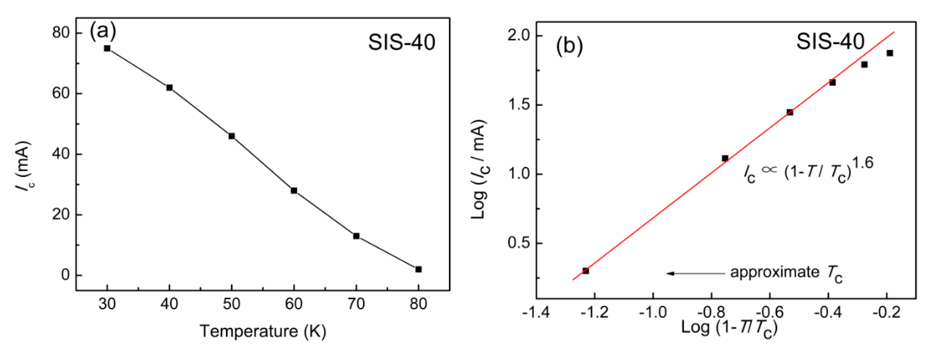
From Figure 7, the critical current value Ic can be acquired from the I–V curve of the SIS-40 sample at each temperature, and the corresponding Ic versus temperature curve is displayed in Figure 8a. It can be seen that Ic gradually decreases, nonlinearly, with increasing temperature. Generally speaking, when the sample temperature approaches the critical transition temperature Tc of the trilayer film, the critical current of the junction acquires an exponential relationship with the temperature, i.e., Ic ∝ (1 − T/Tc)n [21,22].
According to the Ambegaokar–Baratoff’s prediction, the critical current, Ic, of a superconductor/insulator/superconductor (SIS) tunnel junction at a temperature T is [23]:
where kB is the Boltzmann constant, Rn is the normal state zero-bias resistance of the junction and 2Δ is the energy gap of the (identical) superconducting electrodes. For the standard BCS prediction 2Δ(0) = 3.53 × kB × Tc [24].
The above model does not account for the ability of the supercurrent to suppress the gap parameter. To correct this deficiency, a Ginzburg–Landau approach was used to account for current-induced gap suppression. After correction, the critical current near Tc is [25]:
According to the Equations (2) and (4), one can know that Ic is proportional to (1 − T/Tc) for a SIS tunnel junction near Tc.
For the SIS-40 samples, the Tc was ~85 K. By taking the values on the abscissa in Figure 8a, transforming them into 1 − (T/Tc), and then calculating their logarithm, as well as the logarithm of the ordinate values, the log Ic versus log (1 − T/Tc) curve can be obtained, as shown in Figure 8b. By fitting linearly several data points near Tc (>0.5 Tc) it can be seen that, in the range of temperatures ~50–80 K, log Ic and log (1 − T/Tc) show a good linear relationship, with the correlation coefficient R2 reaching 0.99818. The slope of the corresponding linear fit represents the n value, which is 1.6. For the SIS tunnel junction, Ic has a linear relationship with the temperature T, i.e., n = 1. The n value obtained in this experiment is 1.6, indicating that the mechanism for the superconducting current phenomenon in the SIS-40 sample is not caused by the tunneling effect of the SIS junction. However, n = 1.6 is similar to the results reported by Bailey and Aminov, indicating that this characteristic index is related to the point contact between the YBCO layers in the sample [27,28]. In addition, Goodyear and Schneider pointed out that the n value of nano-microbridge junctions is generally in the range of ~1.2–1.9 [29,30]. Therefore, the non-linear characteristics of the I–V curve in Figure 8 are related to the weak connection of the point contact and the microbridge between the top and bottom YBCO layers.
4. Conclusions
The trilayer YBCO/LAO/YBCO heterogeneous film structure was successfully prepared on the LAO single crystal substrate via the sol-gel method. By studying the effect of the intermediate LAO layer thickness on the superconductivity of the heterogeneous film, the following conclusions were obtained:
- The top and bottom YBCO layers in the trilayer film have superconducting properties, with an initial transition temperature of ~90 K, and a resistance that eventually returns to zero, thus showing superconducting performance.
- When the LAO middle layer is sufficiently thin (below 20 nm), the trilayer film shows a high Jc (~3 kA/cm2), which is similar to that of the single-layer YBCO film. When the nominal thickness of the middle LAO layer is 40 nm, the trilayer exhibits I–V characteristics similar to the DC Josephson effect, and its Ic vs. T relationship indicates the presence of point contacts and micro-bridge weak connections in the trilayer film. Finally, when the nominal thickness of the middle LAO film is 70 nm, the superconducting current of the YBCO layer can be isolated in the heterogeneous film, which is useful for the preparation of superconducting circuit integrated devices.
Author Contributions
C.W. conceived and did the experiments and wrote the preliminary version of the paper. Y.W. discussed the results with C.W. and revised the paper. All authors have read and agreed to the published version of the manuscript.
Funding
The work was supported by the Sichuan Provincial Key Laboratory of Comprehensive Utilization of Vanadium and Titanium Resources (Grant No. 2018FTSZ30), Platform Construction Project of Panzhihua City (Grant No. 20180816) and the Major Research Projects in the Experimental Area of Sichuan Province (Grant No. 1840STC30696/01).
Conflicts of Interest
The authors declare no conflict of interest.
References
- Rauch, W.; Behner, H.; Gieres, G.; Sipos, B.; Seeböck, R.; Eibl, O.; Kerner, R.; Sölkner, G.; Gornik, E. Sputtering of YBa2Cu3O7− δ/NdAlO3/YBa2Cu3O7− δ trilayers. Appl. Phys. Lett. 1992, 60, 3304–3306. [Google Scholar] [CrossRef]
- Masterov, D.V.; Parafin, A.E.; Revin, L.S.; Chiginev, A.V.; Pankratov, A.L. YBa2Cu3O7−δ long Josephson junctions on bicrystal Zr1−xYxO2 substrates fabricated by preliminary topology masks. Supercond. Sci. Technol. 2017, 30, 025007. [Google Scholar] [CrossRef]
- Revin, L.S.; Pankratov, A.L.; Masterov, D.V.; Parafin, A.E.; Pavlov, S.A.; Alexander, C.; Skorokhodov, E.V. Features of long YBCO josephson junctions fabricated by preliminary topology mask. IEEE Trans. Appl. Supercond. 2018, 28, 1–5. [Google Scholar] [CrossRef]
- Tsuchiya, R.; Kawasaki, M.; Kubota, H.; Nishino, J.; Sato, H.; Akoh, H.; Koinuma, H. YBa2Cu3O7−δ trilayer junction with nm thickPrGaO3 barrier. Appl. Phys. Lett. 1997, 71, 1570–1572. [Google Scholar] [CrossRef]
- Moeckly, B.H. All Ya–Ba–Cu–O c-axis trilayer interface-engineered Josephson junctions. Appl. Phys. Lett. 2001, 78, 790–792. [Google Scholar] [CrossRef]
- Liu, Y.; Chen, X.; Chen, J.; Yao, W.; Liu, L.; Du, G. Opreparation and performance characterization of Superconducting YBa2Cu3O7−δ-Y2O3 multi-layer thin film. Chin. J. Low. Temp. Phys. 2012, 34, 46–49. [Google Scholar]
- Foltyn, S.R.; Civale, L.; Macmanus-Driscoll, J.L.; Jia, Q.X.; Maiorov, B.; Wang, H.; Maley, M. Materials science challenges for high-temperature superconducting wire. Nat. Mater. 2007, 6, 631–642. [Google Scholar] [CrossRef]
- Maiorov, B.; Baily, S.; Zhou, H.; Ugurlu, O.; Kennison, J.; Dowden, P.; Holesinger, T.; Foltyn, S.; Civale, L. Synergetic combination of different types of defect to optimize pinning landscape using BaZrO3-doped YBa2Cu3O7. Nat. Mater. 2009, 8, 398–404. [Google Scholar]
- Mele, P.; Matsumoto, K.; Ichinose, A.; Mukaida, M.; Kita, R. Systematic study of the BaSnO3 insertion effect on the properties of YBa2Cu3O7−x films prepared by pulsed laser ablation. Supercond. Sci. Technol. 2008, 21, 125017. [Google Scholar] [CrossRef]
- Li, L.; Zhao, G.; Xu, H.; Wu, N.; Chen, Y. Influences of Y2O3 nanoparticle additions on the microstructure and superconductivity of YBCO films derived from low-fluorine solution. Mater. Chem. Phys. 2011, 127, 91–94. [Google Scholar] [CrossRef]
- Wang, X.; Wu, J.Z. Effect of interlayer magnetic coupling on the Jc of YBa2Cu3O7/insulator/ YBa2Cu3O7 trilayers. Appl. Phys. Lett. 2006, 88, 062513. [Google Scholar] [CrossRef]
- Foltyn, S.R.; Wang, H.; Civale, L.; Jia, Q.X.; Arendt, P.N.; Maiorov, B.; Li, Y.; Maley, M.P.; MacManus-Driscoll, J.L. Overcoming the barrier to 1000 A/cm width superconducting coatings. Appl. Phys. Lett. 2005, 87, 162505. [Google Scholar] [CrossRef]
- Pan, A.V.; Pysarenko, S.; Dou, S.X. Drastic improvement of surface structure and current-carrying ability in YBa2Cu3O7 films by introducing multilayered structure. Appl. Phys. Lett. 2006, 88, 232506. [Google Scholar] [CrossRef] [Green Version]
- Locquet, J.P.; Perret, J.; Fompeyrine, J.; Maechler, E.; Seo, J.W.; Tendeloo, G.V. Doubling the critical temperature of La1.9Sr0.1CuO4 using epitaxial strain. Nature 1998, 394, 453–456. [Google Scholar] [CrossRef]
- Wu, C.; Zhao, G.; Lei, L.; Zhao, R.; Qu, G. Effect of Y2O3 buffer layer on superconducting transition temperature of YBCO films. Chin. J. Low. Temp. Phys. 2014, 36, 81–85. [Google Scholar]
- Horwitz, J.S.; Cotell, C.M.; Chrisey, D.B.; Pond, J.M.; Osofsky, M.S. Origins of conductive losses at microwave frequencies in YBa2Cu3O7−δ/LaAlO3/YBa2Cu3O7−δ trilayers deposited by pulsed laser deposition. J. Supercond. 1994, 7, 965–969. [Google Scholar] [CrossRef]
- Wu, C.; Wang, Y. Enhancement of critical current density by establishing a YBa2Cu3O7−x/LaAlO3/ YBa2Cu3O7−x quasi-trilayer architecture using the sol-gel method. Coatings 2019, 9, 437. [Google Scholar] [CrossRef] [Green Version]
- Chen, Y.; Wu, C.; Zhao, G.; You, C. An advanced low-fluorine solution route for fabrication of high-performance YBCO superconducting films. Supercond. Sci. Technol. 2012, 25, 069501. [Google Scholar] [CrossRef] [Green Version]
- Wu, C.; Zhao, G.; Lei, L. Enhancement of critical current density in superconducting YBa2Cu3O7−x films by nanostructure development of substrate surface using sol-gel method. J. Sol-Gel. Sci. Techn. 2013, 67, 203–207. [Google Scholar] [CrossRef]
- Jia, Y.; Hua, J.; Crabtree, G.W.; Kwok, W.K.; Welp, U.; Malozemoff, A.P.; Rupich, M.; Fleshler, S. C-axis critical current density of second-generation YBCO tapes. Supercond. Sci. Technol. 2010, 23, 115017. [Google Scholar] [CrossRef]
- Seidel, P.; Schmidl, F.; Pfuch, A.; Schneidewind, H.; Heinz, E. Investigations on high-TC thin film intrinsic stacked Josephson junctions. Supercond. Sci. Technol. 1999, 9, A9–A13. [Google Scholar] [CrossRef]
- Zalecki, R.; Woch, W.M.; Chrobak, M.; Koldziejczyk, A. Resistance and AC Susceptibility of YBCO 1:2:3 Films on Silver Substrates. Acta Phys. Pol. A 2012, 121, 850–853. [Google Scholar] [CrossRef]
- Ambegaokar, V.; Baratoff, A. Tunneling between superconductors. Phys. Rev. Lett. 1963, 10, 486–489. [Google Scholar] [CrossRef]
- Delin, K.A.; Kleinsasser, A.W. Stationary properties of high-critical-temperature proximity effect Josephson junctions. Supercond. Sci. Technol. 1996, 9, 227–269. [Google Scholar] [CrossRef]
- Clem, J.R.; Bumble, B.; Raider, S.I.; Gallagher, W.J.; Shih, Y.C. Ambegaokar-Baratoff—Ginzburg-Landau crossover effects on the critical current density of granular superconductors. Phys. Rev. B 1987, 35, 6637–6642. [Google Scholar] [CrossRef] [PubMed]
- Tinkham, M. Introducton to Superconductivity, 2nd ed.; Dover Publications: Mineola, NY, USA, 1996; pp. 63–64. [Google Scholar]
- Bailey, A.; Alvarez, G.; Puzzer, T.; Town, S.L.; Russell, G.J.; Taylor, K.N.R. Josephson behaviour for high critical current density YBCO+Ag thick films on YSZ substrates. Physica C 1990, 167, 133–138. [Google Scholar] [CrossRef]
- Aminov, B.A.; Brandt, N.B.; Thuy, N.M.; Ponomarev, Y.G.; Sudakova, M.V.; Kaul, A.R.; Graboi, I.E.; Tretiakov, Y.D.; Wittig, J.; Kobeleva, S.P. Temperature dependence of the critical current in YBa2Cu3O7−δ and Bi2Sr2Ca1Cu2O8 Josephson junctions. Physica C 1989, 160, 505–510. [Google Scholar] [CrossRef]
- Goodyear, S.W.; Chew, N.G. Vertical c-axis microbridge junctions in YBa2Cu3O7/PrBa2Cu3O7 thin films. IEEE Trans. Appl. Supercond. 1995, 5, 3143–3146. [Google Scholar] [CrossRef]
- Schneider, J.; Kohlstedt, H.; Wordenweber, R. Nanobridges of optimized YBa2Cu3O7 thin films for superconducting flux-flow type devices. Appl. Phys. Lett. 1993, 63, 2426–2428. [Google Scholar] [CrossRef]
Figure 1.
Diagrammatic drawing for measuring Tc of top and bottom YBa2Cu3O7−x (YBCO) layer (a) and I–V characteristics of the trilayer films (b).
Figure 1.
Diagrammatic drawing for measuring Tc of top and bottom YBa2Cu3O7−x (YBCO) layer (a) and I–V characteristics of the trilayer films (b).

Figure 2.
XRD patterns of LaAlO3 (LAO) films grown on Si (a) and LAO (b) substrates.

Figure 3.
XRD patterns of the YBCO/LAO/YBCO trilayer films.

Figure 4.
R–T curves of top and bottom YBCO layers in the YBCO/LAO/YBCO trilayer film with different LAO interlayer thickness. (a) 0; (b) 20 nm; (c) 40 nm; (d) 70 nm. The inset in (d) is a partial enlargement in the superconducting transition region, showing the process for acquiring Tc.
Figure 4.
R–T curves of top and bottom YBCO layers in the YBCO/LAO/YBCO trilayer film with different LAO interlayer thickness. (a) 0; (b) 20 nm; (c) 40 nm; (d) 70 nm. The inset in (d) is a partial enlargement in the superconducting transition region, showing the process for acquiring Tc.

Figure 5.
I–V curves of the YBCO/YBCO (SS) trilayer and YBCO/LAO/YBCO (SIS-20) trilayer films with the LAO interlayer thickness of 20 nm.
Figure 5.
I–V curves of the YBCO/YBCO (SS) trilayer and YBCO/LAO/YBCO (SIS-20) trilayer films with the LAO interlayer thickness of 20 nm.

Figure 6.
I–V curves of the YBCO/LAO (70 nm)/YBCO trilayer film.

Figure 7.
I–V curves of the YBCO/LAO (40 nm)/YBCO trilayer under different temperatures.

Figure 8.
Curves showing the variation of Ic for the YBCO/LAO (40 nm)/YBCO trilayer with the test temperature: (a) Ic vs. T, (b) logIc vs log (1 − T/Tc).
Figure 8.
Curves showing the variation of Ic for the YBCO/LAO (40 nm)/YBCO trilayer with the test temperature: (a) Ic vs. T, (b) logIc vs log (1 − T/Tc).


Table 1.
Physical parameters of YBCO, LaAlO3 and Si.
| Materials | Lattice Type | Lattice Parameter (nm) | Thermal Expansion Coefficient (10−6/K) |
|---|---|---|---|
| YBCO | perovskite | a = 0.382, b = 0.389, c = 11.68 | 13.4 |
| LaAlO3 | perovskite (pseudocubic) | a = b = c = 0.379 | 10.0 |
| Si | cubic diamond | a = b = c = 0.543 | 2.5 |
Table 2.
Superconducting transition parameters of the YBCO layers in the YBCO/LAO/YBCO trilayer films.
Table 2.
Superconducting transition parameters of the YBCO layers in the YBCO/LAO/YBCO trilayer films.
| Sample | YBCO Layers | Tc/K | ΔTc/K | Tc0/K |
|---|---|---|---|---|
| SS | top YBCO | 90.2 | 1.1 | 88.4 |
| bottom YBCO | 89.8 | 2.4 | 85.7 | |
| SIS-20 | top YBCO | 89.9 | 1.5 | 87.8 |
| bottom YBCO | 89.7 | 3.3 | 82.9 | |
| SIS-40 | top YBCO | 88.6 | 2.3 | 84.5 |
| bottom YBCO | 88.2 | 3.6 | 81.1 | |
| SIS-70 | top YBCO | 87.2 | 2.3 | 80.1 |
| bottom YBCO | 83.5 | 4.2 | 72.5 |
© 2020 by the authors. Licensee MDPI, Basel, Switzerland. This article is an open access article distributed under the terms and conditions of the Creative Commons Attribution (CC BY) license (http://creativecommons.org/licenses/by/4.0/).
Share and Cite
MDPI and ACS Style
Wu, C.; Wang, Y. Trilayer Films of YBa2Cu3O7−x/LaAlO3/YBa2Cu3O7−x with Superconducting Properties Prepared via Sol-Gel Method. Coatings 2020, 10, 686. https://0-doi-org.brum.beds.ac.uk/10.3390/coatings10070686
AMA Style
Wu C, Wang Y. Trilayer Films of YBa2Cu3O7−x/LaAlO3/YBa2Cu3O7−x with Superconducting Properties Prepared via Sol-Gel Method. Coatings. 2020; 10(7):686. https://0-doi-org.brum.beds.ac.uk/10.3390/coatings10070686
Chicago/Turabian StyleWu, Chuanbao, and Yunwei Wang. 2020. "Trilayer Films of YBa2Cu3O7−x/LaAlO3/YBa2Cu3O7−x with Superconducting Properties Prepared via Sol-Gel Method" Coatings 10, no. 7: 686. https://0-doi-org.brum.beds.ac.uk/10.3390/coatings10070686
Note that from the first issue of 2016, this journal uses article numbers instead of page numbers. See further details here.