
Highly Conductive Co-Doped Ga2O3:Si-In Grown by MOCVD


Center for Quantum Devices, Department of Electrical and Computer Engineering, Northwestern University, Evanston, IL 60208, USA
*
Author to whom correspondence should be addressed.
Coatings 2021, 11(3), 287; https://0-doi-org.brum.beds.ac.uk/10.3390/coatings11030287
Submission received: 17 February 2021
/
Revised: 23 February 2021
/
Accepted: 27 February 2021
/
Published: 2 March 2021
(This article belongs to the Special Issue Thin Films and Nanostructures by MOCVD: Fabrication, Characterization and Applications)
Abstract
:We report a highly conductive gallium oxide doped with both silicon and indium grown on c-plane sapphire substrate by MOCVD. From a superlattice structure of indium oxide and gallium oxide doped with silicon, we obtained a highly conductive material with an electron hall mobility up to 150 cm2/V·s with the carrier concentration near 2 × 1017 cm−3. However, if not doped with silicon, both Ga2O3:In and Ga2O3 are highly resistive. Optical and structural characterization techniques such as X-ray, transmission electron microscope, and photoluminescence, reveal no significant incorporation of indium into the superlattice materials, which suggests the indium plays a role of a surfactant passivating electron trapping defect levels.
1. Introduction
Gallium oxide (Ga2O3) has drawn much attention due to its potential for realizing next generation ultra-wide band gap (UWBG) electronic/optoelectronic device applications such as high-power transistors or ultraviolet (UV) solar blind photodetectors (SBPD). Of five possible different polymorphic forms (α-, β-, γ-, δ-, and κ) [1,2], single crystal β-Ga2O3 exhibits a relatively high breakdown voltage compared with those of other wide bandgap materials, such as GaN or SiC. In addition, alloying with other elements such as indium, aluminum or magnesium allows for band gap engineering within the ultraviolet C light (UVC) solar blind band (200–280 nm) [3,4,5]. These potential advantages, along with the presence of commercially available single crystal substrates, have drawn considerable interest in utilizing β-Ga2O3 in many important technological applications from transparent electrodes, thin film transistors and gas sensors to solar blind photodetectors and light-emitting diodes (LED) emitting in UVC band [6]. Besides the commonly investigated β-Ga2O3, there has been a growing interest in the metastable phase of Ga2O3, such as κ or ε-phase, as those phases also exhibit a wide band gap energy near 4.8 eV, in addition to the fact that they are often readily obtained by heteroepitaxy when grown on hexagonal substrates such as MgO or Al2O3 [7,8,9,10,11,12,13]. Furthermore, κ-Ga2O3 is predicted to possess a large spontaneous polarization value (~26 µC/cm2) along c-direction, which have attracted a significant interest in scientific community [14]. In a recent report [15], we also have shown that κ-Ga2O3 can be grown on c-plane sapphire substrates. In addition, we have reported that the phase of as-grown κ-Ga2O3 on c-plane sapphire substrates can be changed to β-phase upon annealing at 1000 °C [16]. This as-grown κ-Ga2O3 was highly resistive to be applied for practical electronic applications. In order to realize high-performance electronics, controlling conductivity of epitaxial layers is an important factor. For instance, both a highly resistive buffer layer and a subsequently grown conductive layer are the structure commonly employed for electronic devices with high performance [17,18]. Although a conductive metastable ε-Ga2O3 grown by metal organic chemical vapor deposition (MOCVD) was presented, the reported hall mobility at room temperature was in the range of 1~5 cm2/V·s with the electron concentration near 3 × 1018 cm−3 [19]. These mobility values are not as high as those reported from β-Ga2O3 [20,21], which resulted in a relatively high device performance. In this present work, we demonstrate a highly conductive co-doped Ga2O3:Si-In with a high electron mobility up to ~150 cm2/V·s at room temperature grown by MOCVD on c-plane sapphire substrate, with carrier concentration of 2 × 1017 cm−3.
2. Materials and Methods
We grew different superlattice structures consisting of oxide layers with various doping at 690 °C under H2 carrier gas using Trimethyl-gallium (TMGa) and Trimethyl-indium (TMIn), pure H2O vapor and Silane (SiH4) as Ga, In, O and Si precursors, respectively, grown by Aixtron horizontal AIX200/4 MOCVD reactor. The growth details for the materials as well as conditions of post ex situ and in situ annealing can be found in our previous report [16]. Detail information about different superlattice structures is summarized in Table 1.
3. Results and Discussion
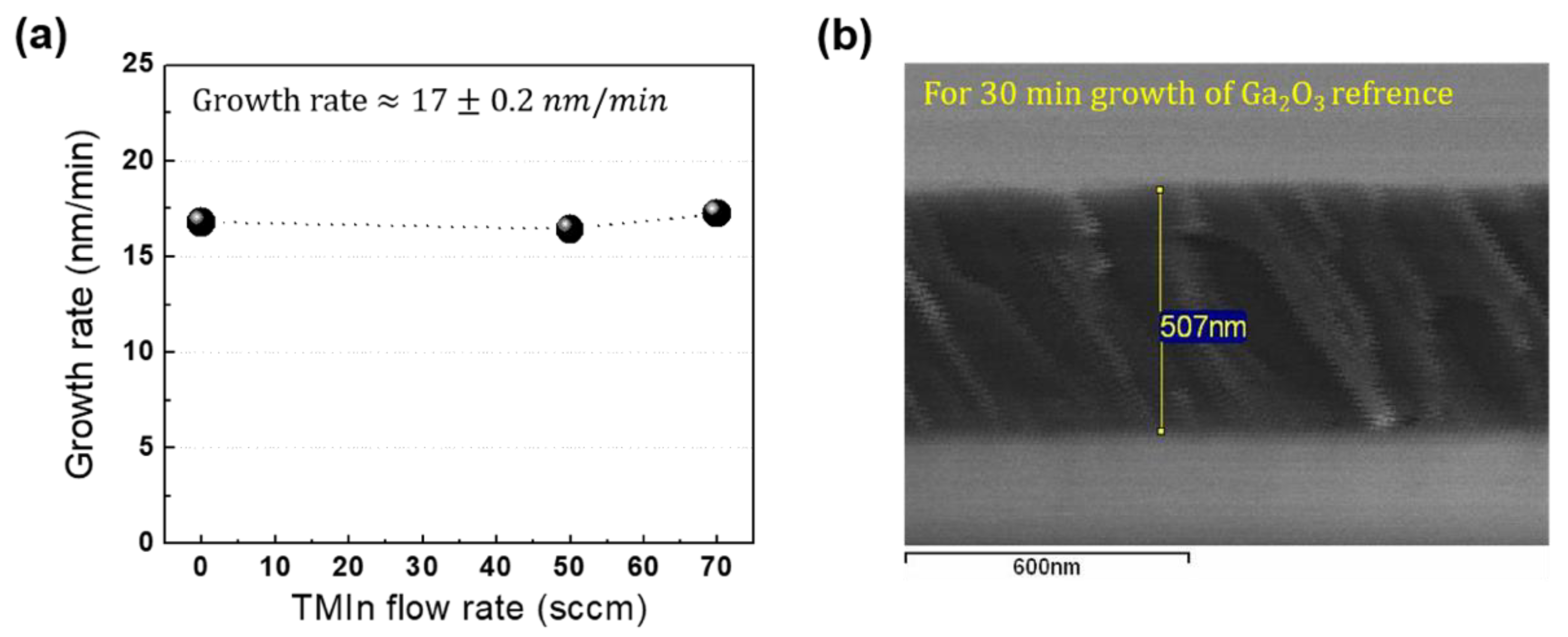
We performed several characterizations for the samples listed in Table 1. At first, through scanning electron microscope (SEM), we measured the total thickness of the superlattice structures shown in Figure 1. All of the deposited superlattice layers have an equivalent growth rate regardless of the TMIn flow rate during the growth. For example, the reference Ga2O3:Si (Structure 1) was deposited with a rate of 16.8 nm/min while that of Ga2O3:Si/(InxGa1−x)2O3:Si (Structure 4) was 17.2 nm/min showing the error range of 0.2 nm/min. This possibly indicates that In2O3 was not formed or the growth of In2O3 was formed in non-layer-by-layer fashion.
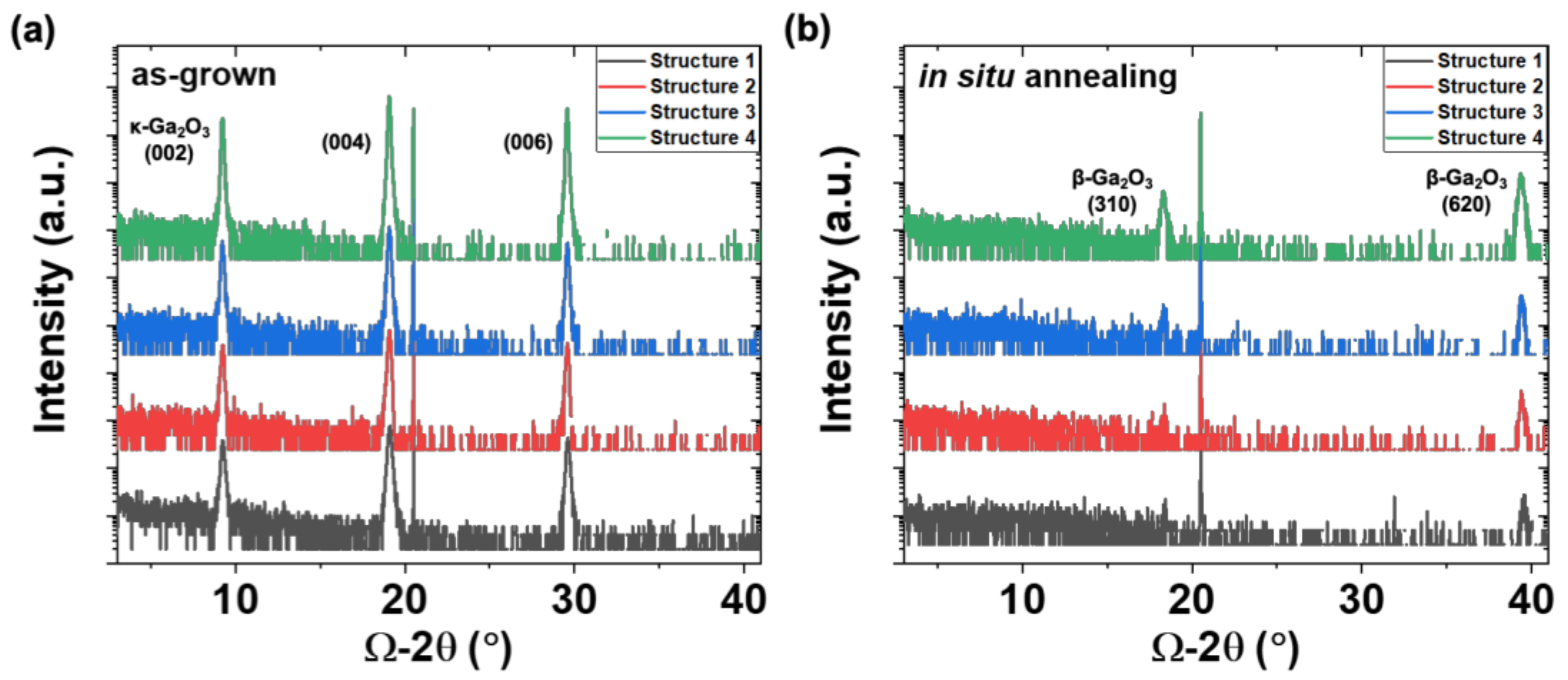
The X-ray diffraction (XRD) patterns shown in Figure 2 also support the fact that indium would not be properly formed as a layer. All the as-grown samples exhibit the same peak positions corresponding to κ-Ga2O3 (002), (004), and (006) reflections. Particularly, neither superlattice satellite peaks nor peak position shift were observed from the superlattice structures in spite of the fact that TMIn was supplied during the growth. This result indicates that the incorporated indium is small enough not to cause a change in the out of plane lattice parameter. These samples also showed the evidence of phase transition from κ- to β-phase upon annealing at 1000 °C, which is in agreement with our previous study [16]. Although phase transition occurred after the annealing process, no evidence of the peak shifts in either (310) or (620) peaks were observed. If In2O3 was grown and subsequent indium diffusion happened after the annealing at 1000 °C, one would expect to observe peak shift in (310) and (620) peaks as the diffused indium atoms will replace Ga atoms and the lattice parameter should subsequently change, which was not observed in our study. This observation suggests that the incorporated indium is in a small degree since substantial indium incorporation should result in a higher growth rate as a result of increased group III molar flow rate or cause to make peak shifts in XRD data.
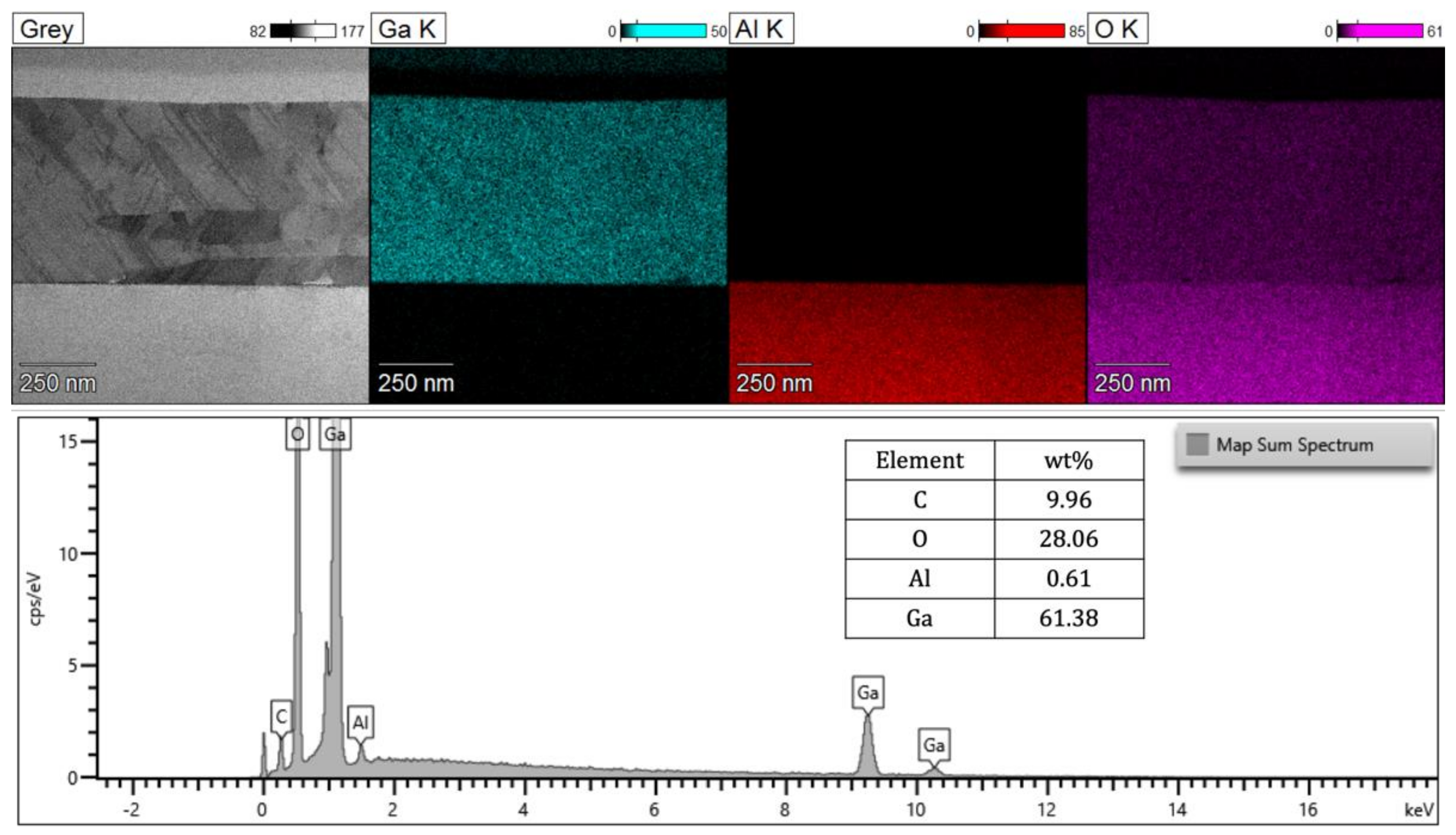
In order to further investigate the indium incorporation in the superlattice structures, energy-dispersive X-ray spectroscopy (EDS) taken along with scanning transmission electron miscroscopic ((S)TEM)) analysis was carried out for the superlattice sample grown with 70 sccm (standard cubic centimeters per minute) of TMIn flow rate (Structure 3). As shown in Figure 3, no evidence of indium containing nanostructure was observed below its detection limit (0.1 wt.%), which is in line with the identical multiple peaks in the XRD patterns as well as the nearly constant growth rate. Therefore, based on the aforementioned characterization data, we confirmed that no significant amount of indium incorporation has been found in all of the superlattice structure.
Although the indium was not incorporated within the superlattice structures, we found remarkable improvement in electrical characteristics of samples. Table 2 summarizes the electrical performance measured from all different types of films (From Structure 1 to Structure 4). In contrast to the electrically resistive as-grown κ-Ga2O3:Si (ρ > 2000 Ω·cm) noted as Structure 1, all of the as-grown superlattice structures (Structure 2,3,4) exhibited a high conductivity with the resistivity as low as ρ = 0.69 Ω·cm. For instance, the hall mobility of 150 cm2/V·s was obtained from the In2O3:Si based superlattice structure grown with 70 sccm of TMIn flow rate (Structure 3), which is higher by several times than the any other values measured from other structures. These as-grown In2O3 based superlattice samples (Structure 2 and Structure 3) exhibited generally higher electron mobilities by a factor of 3~15, in comparison to the values obtained from the Ga2O3:Si/(InxGa1−x)2O3:Si based superlattice layer (Structure 4), with the electron concentration ranging from 2 × 10¹⁷ to 1.3 × 1018 cm−3. This phenomenon can be explained by the previous experiments that indium has been known as an effective surfactant to improve dislocation densities, surface roughness, carrier mobilities and activated carrier densities within GaN-based system [22,23,24,25,26,27]. In the past, we reported that by adding TMIn during AlGaN growth, remarkable improvement in hall mobility has been observed since TMIn helps to relieve strains, making crack-free growth of AlGaN on sapphire substrate [22,23]. Although our superlattice structures are formed without having cracks on surface, TMIn showed similar effects in oxide growth as well, leading to the improved conductivity. On the other hand, it must be noted that all of the superlattice structures grown without silane as a dopant resulted in a high resistivity before (>11800 Ω·cm) and even after annealing (>9050 Ω·cm). This result has alluded to the fact that the silicon plays a role as a shallow donor, while indium acts as a surfactant which helps enhance the activation of silicon within the metastable κ-Ga2O3.
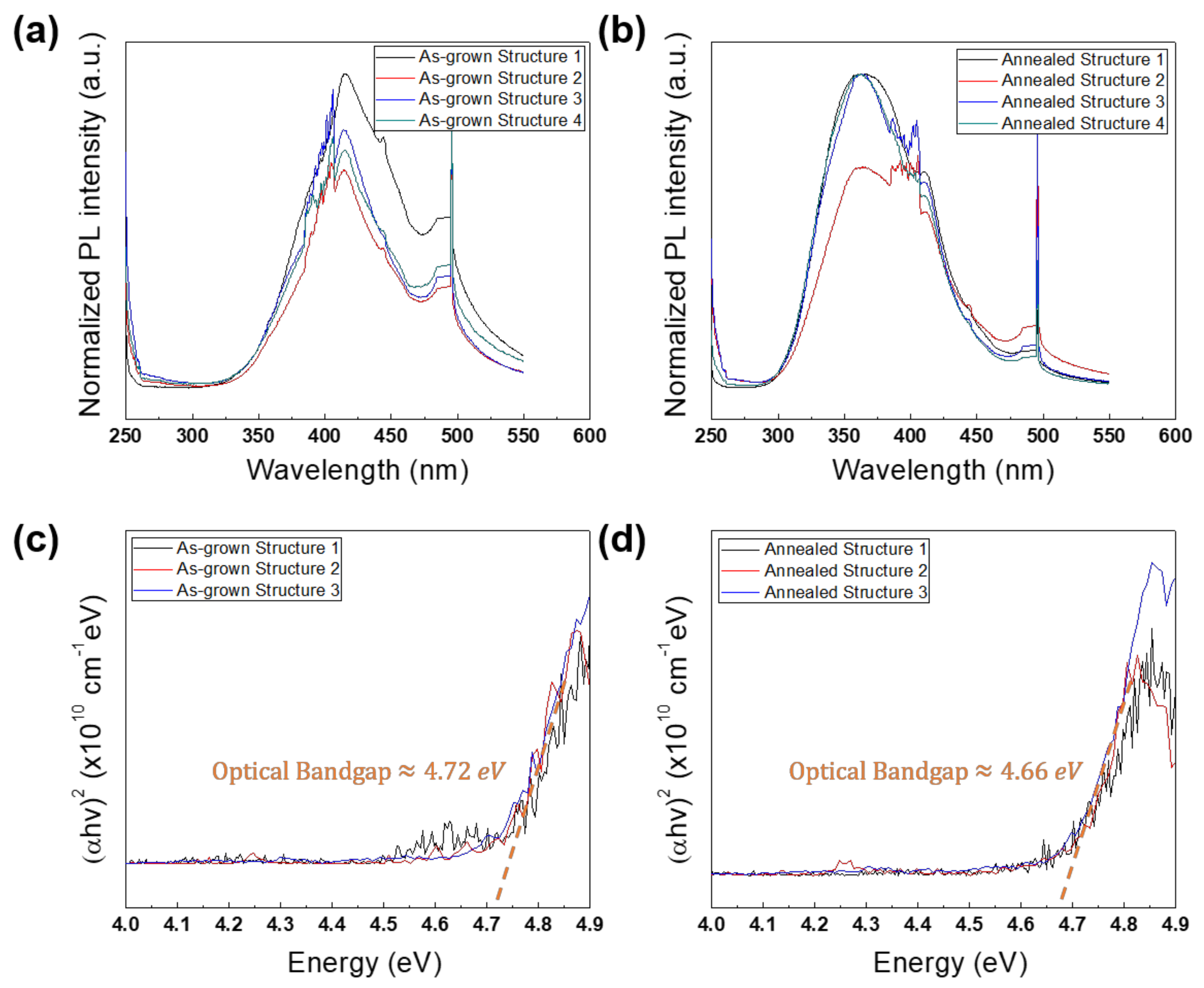
Normalized photoluminescence (PL) spectra were taken from all of the as-grown (Figure 4a) and annealed (Figure 4b) superlattice samples listed in Table 1. After annealing process and the subsequent phase transition to β phase, the peak position has shift to near 360 nm which is similar to β-phase Ga2O3 substrate while the peak around 420 nm seems to be related to κ phase, in accordance with our previous results [16]. Apart from the change in the PL peak, other noticeable traits depending on the amount of TMIn during the growth have not been observed, supporting the fact that indium acts as a surfactant rather than being deposited. Although we found the PL peak might be related to the phase of materials, discovering the origin of PL emission peaks is our ongoing research and thus further investigation is required to provide clear interpretation of PL data.
Transmission measurement had also been conducted in order to calculate the optical bandgap of the samples. We discovered the evidence of a decrease in bandgap energy as a result of the phase transition caused by the annealing process at 1000 °C. The (αE)2 plots demonstrated that the phase variation from κ- to β-phase leads to a decrease in optical energy bandgap for the superlattice structures. Specifically, through a linear fitting, an extracted direct bandgap energy of 4.72 eV for the as-grown samples was measured whereas the optical bandgap energy of the annealed superlattice structures was reduced to 4.66 eV, indicating that the phase transition may have an influence on the direct bandgap energy. However, similar to the previous observation in PL, regardless of the supply of TMIn during the growth, none of the superlattice samples had represented different optical characteristics compared to the reference. Therefore, based on the PL and transmission measurement data, it suggests that the energy gap of β-phase layers is lower than the one of κ-phase Ga2O3-based material systems.
4. Conclusions
Highly conductive co-doped Ga2O3:Si-In films grown on c-plane sapphire substrate were demonstrated with a significantly high electron mobility. Structural characterization represented that under H2 condition as a carrier gas, the samples were grown having metastable κ-phase whereas the annealed samples became β-phase in either case of whether we doped with silicon or not. When the materials were not doped with silicon, both as-grown and annealed thin films had a high resistivity. Also, even if silicon was added as a dopant during the growth, the as-grown layers still had a high resistivity. On the other hand, when doped with silicon and supply the TMIn during the growth, a significantly improved electron hall mobility up to 150 cm2/V·s had been observed in as-grown samples, showing a tendency that a higher flow of TMIn leaded to an increase in the mobility. Other characterizations such as cross-sectional SEM, and EDX analysis indicate that no significant fractional indium incorporation takes places. Rather, the TMIn flow during the various superlattice growths leads to indium at the growth front acting as a surfactant enhancing the electron hall mobilities. This observation indicates the silicon is a shallow donor within co-doped Ga2O3:Si-In while indium acts a surfactant which enhances the hall mobility. The findings presented in this report are crucial in realizing high-performance electronic applications such as high-power transistors where the control of electrical conductivity is important.
Author Contributions
Data curation, J.L.; formal analysis, J.L. and L.G.; investigation, J.L.; project administration, M.R.; software, H.K.; validation, J.L.; writing—original draft, J.L. and H.K.; writing—review and editing, J.L. and M.R. All authors have read and agreed to the published version of the manuscript.
Funding
This work is supported by Air Force under agreement of FA9550-19-1-0410.
Institutional Review Board Statement
Not applicable.
Informed Consent Statement
Not applicable.
Data Availability Statement
The data presented in this study are available on request from the corresponding author.
Acknowledgments
This work is supported by Air Force under agreement of FA9550-19-1-0410. The authors would like to acknowledge the support and interest of Ali Sayir of USAF-AFMC AFMCAFOSR/RTB). The (S)TEM characterizations made use of the EPIC facility of Northwestern University’s NUANCE Center, which has received support from the SHyNE Resource (NSF ECCS-2025633), the IIN, and Northwestern′s MRSEC program (NSF DMR-1720139). The authors would like to acknowledge Vinayak P. Dravid, Xiaobing Hu and Kun He as well.
Conflicts of Interest
The authors declare no conflict of interest.
References
- Roy, R.; Hill, V.G.; Osborn, E.F. Polymorphism of Ga2O3 and the system Ga2O3—H2O. J. Am. Chem. Soc. 1952, 74, 719–722. [Google Scholar] [CrossRef]
- Razeghi, M.; Park, J.H.; McClintock, R.; Pavlidis, D.; Teherani, F.H.; Rogers, D.J.; Magill, B.A.; Khodaparast, G.A.; Xu, Y.; Wu, J.; et al. A Review of the growth, doping, and applications of β-Ga2O3 thin films. Proc. SPIE 2018, 10533, 105330R1-24. [Google Scholar]
- Anhar Uddin Bhuiyan, A.F.M.; Feng, Z.; Johnson, J.M.; Huang, H.L.; Hwang, J.; Zhao, H. MOCVD Epitaxy of ultrawide bandgap β-(AlxGa1−x)2O3 with high-Al composition on (100) β-Ga2O3 substrates. Cryst. Growth Des. 2020, 20, 6722–6730. [Google Scholar] [CrossRef]
- Hatipoglu, I.; Mukhopadhyay, P.; Alema, F.; Sakthivel, T.S.; Seal, S.; Osinsky, A.; Schoenfeld, W.V. Tuning the responsivity of monoclinic solar-blind photodetectors grown by metal organic chemical vapor deposition. J. Phys. D Appl. Phys 2020, 53, 454001. [Google Scholar] [CrossRef]
- Bi, X.; Wu, Z.; Huang, Y.; Tang, W. Stabilization and enhanced energy gap by Mg doping in ε-phase Ga2O3 thin films. AIP Adv. 2018, 8, 025008. [Google Scholar] [CrossRef] [Green Version]
- Teherani, F.H.; Rogers, D.J.; Sandana, V.E.; Bove, P.; Ton-That, C.; Lem, L.L.C.; Chikoidze, E.; Neumann-Spallart, M.; Dumont, Y.; Huynh, T.; et al. Investigations on the substrate dependence of the properties in nominally-undoped beta-Ga2O3 thin films grown by PLD. Proc. SPIE 2017, 10105, 101051R. [Google Scholar]
- Shinohara, D.; Fujita, S. Heteroepitaxy of corundum-structured α-Ga2O3 thin films on α-Al2O3 substrates by ultrasonic mist chemical vapor deposition. Jpn. J. Appl. Phys. 2008, 47, 7311–7313. [Google Scholar] [CrossRef]
- Kawaharamura, T.; Dang, G.T.; Furuta, M. Successful growth of conductive highly crystalline Sn-doped α-Ga2O3 thin films by fine-channel mist chemical vapor deposition. Jpn. J. Appl. Phys. 2012, 51, 040207. [Google Scholar] [CrossRef]
- Sun, H.; Li, K.H.; Castanedo, C.T.; Okur, S.; Tompa, G.S.; Salagaj, T.; Lopatin, S.; Genovese, A.; Li, X. HCl flow-induced phase change of α-, β-, and ε-Ga2O3 films grown by MOCVD. Cryst. Growth Des. 2018, 18, 2370–2376. [Google Scholar] [CrossRef]
- Boschi, F.; Bosi, M.; Berzina, T.; Buffagni, E.; Ferrari, C.; Fornari, R. Hetero-epitaxy of ε-Ga2O3 layers by MOCVD and ALD. J. Cryst. Growth 2016, 443, 25–30. [Google Scholar] [CrossRef]
- Yao, Y.; Okur, S.; Lyle, L.A.; Tompa, G.S.; Salagaj, T.; Sbrockey, N.; Davis, R.F.; Porter, L.M. Growth and characterization of α-, β-, and ϵ-phases of Ga2O3 using MOCVD and HVPE techniques. Mater. Res. Lett. 2018, 6, 268–275. [Google Scholar] [CrossRef] [Green Version]
- Park, J.H.; McClintock, R.; Razeghi, M. Ga2O3 metal-oxide-semiconductor field effect transistors on sapphire substrate by MOCVD. Semicond. Sci. Technol. 2019, 34, 08LT01. [Google Scholar] [CrossRef]
- McClintock, R.; Jaud, A.; Gautam, L.; Razeghi, M. Solar-blind photodetectors based on Ga2O3 and III-nitrides. Proc. SPIE 2020, 11288, 1128803. [Google Scholar]
- Kim, J.; Tahara, D.; Miura, Y.; Kim, B.G. First-principle calculations of electronic structures and polar properties of (κ, ε)-Ga2O3. Appl. Phys. Express 2018, 11, 061101. [Google Scholar] [CrossRef]
- Xu, Y.; Park, J.H.; Yao, Z.; Wolverton, C.; Razeghi, M.; Wu, J.; Dravid, V.P. Strain-induced metastable phase stabilization in Ga2O3 thin films. ACS Appl. Mater. Interfaces 2019, 11, 5536–5543. [Google Scholar] [CrossRef]
- Lee, J.; Kim, H.; Gautam, L.; He, K.; Hu, X.; Dravid, V.P.; Razeghi, M. Study of phase transition in MOCVD grown Ga2O3 from κ to β phase by ex situ and in situ annealing. Photonics 2021, 8, 17. [Google Scholar] [CrossRef]
- Wong, M.H.; Sasaki, K.; Kuramata, A.; Yamakoshi, S.; Higashiwaki, M. Anomalous Fe diffusion in Si-ion-implanted β–Ga2O3 and its suppression in Ga2O3 transistor structures through highly resistive buffer layers. Appl. Phys. Lett. 2015, 106, 032105. [Google Scholar] [CrossRef]
- Joishi, C.; Xia, Z.; McGlone, J.; Zhang, Y.; Arehart, A.R.; Ringel, S.; Lodha, S.; Rajan, S. Effect of buffer iron doping on delta-doped β-Ga2O3 metal semiconductor field effect transistors. Appl. Phys. Lett. 2018, 113, 123501. [Google Scholar] [CrossRef]
- Parisini, A.; Bosio, A.; Montedoro, V.; Gorreri, A.; Lamperti, A.; Bosi, M.; Garulli, G.; Vantaggio, S.; Fornari, R. Si and Sn doping of ε-Ga2O3 layers. APL Mater. 2019, 7, 031114. [Google Scholar] [CrossRef] [Green Version]
- Moser, N.; McCandless, J.; Crespo, A.; Leedy, K.; Green, A.; Neal, A.; Mou, S.; Ahmadi, E.; Speck, J.; Chabak, K.; et al. Ge-doped β-Ga2O3 MOSFETs. IEEE Electron Device Lett. 2017, 38, 775–778. [Google Scholar] [CrossRef]
- Zhang, Y.; Alema, F.; Mauze, A.; Koksaldi, O.S.; Miller, R.; Osinsky, A.; Speck, J.S. MOCVD grown epitaxial β-Ga2O3 thin film with an electron mobility of 176 cm2/V s at room temperature. APL Mater. 2019, 7, 022506. [Google Scholar] [CrossRef] [Green Version]
- McClintock, R.; Yasan, A.; Mayes, K.; Shiell, D.; Darvish, S.R.; Kung, P.; Razeghi, M. High quantum efficiency AlGaN solar-blind p-i-n photodiodes. Appl. Phys. Lett. 2004, 84, 1248–1250. [Google Scholar] [CrossRef]
- Razeghi, M.; Yasan, A.; McClintock, R.; Mayes, K.; Shiell, D.; Darvish, S.R.; Kung, P. Review of III-nitride optoelectronic materials for light emission and detection. Phys. Status Solidi (c) 2004, 1, S141–S148. [Google Scholar] [CrossRef]
- Keller, S.; Heikman, S.; Ben-Yaacov, I.; Shen, L.; DenBaars, S.P.; Mishra, U.K. Indium-surfactant-assisted growth of high-mobility AlN/GaN multilayer structures by metalorganic chemical vapor deposition. Appl. Phys. Lett. 2001, 79, 3449–3451. [Google Scholar] [CrossRef]
- Kyle, E.C.H.; Kaun, S.W.; Young, E.C.; Speck, J.S. Increased p-type conductivity through use of an indium surfactant in the growth of Mg-doped GaN. Appl. Phys. Lett. 2015, 106, 222103. [Google Scholar] [CrossRef]
- Aisaka, T.; Tanikawa, T.; Kimura, T.; Shojiki, K.; Hanada, T.; Katayama, R.; Matsuoka, T. Improvement of surface morphology of nitrogen-polar GaN by introducing indium surfactant during MOVPE growth. Jpn. J. Appl. Phys. 2014, 53, 085501. [Google Scholar] [CrossRef]
- Chen, Y.; Wu, H.; Han, E.; Yue, G.; Chen, Z.; Wu, Z.; Wang, G.; Jiang, H. High hole concentration in p-type AlGaN by indium-surfactant-assisted Mg-delta doping. Appl. Phys. Lett. 2015, 106, 162102. [Google Scholar] [CrossRef]
Figure 1.
(a) The summary of growth rate depending on the Trimethyl-indium (TMIn) flow rate. (b) The cross-sectional SEMs image of Ga2O3 reference growth.
Figure 1.
(a) The summary of growth rate depending on the Trimethyl-indium (TMIn) flow rate. (b) The cross-sectional SEMs image of Ga2O3 reference growth.

Figure 2.
XRD patterns from the various (a) as-grown superlattice structures and (b) the annealed samples listed in Table 1.
Figure 2.
XRD patterns from the various (a) as-grown superlattice structures and (b) the annealed samples listed in Table 1.

Figure 3.
Energy-dispersive X-ray spectroscopy (EDS) analysis performed from the as-grown superlattice structure based on In2O3 grown with 70 sccm of TMIn (Structure 3) through both TEM and SEM.
Figure 3.
Energy-dispersive X-ray spectroscopy (EDS) analysis performed from the as-grown superlattice structure based on In2O3 grown with 70 sccm of TMIn (Structure 3) through both TEM and SEM.

Figure 4.
Photoluminescence spectra from all of the (a) as-grown and (b) annealed superlattice structures. Transmission measurement of (c) as-grown and (d) annealed superlattice layers for obtaining the optical bandgap.
Figure 4.
Photoluminescence spectra from all of the (a) as-grown and (b) annealed superlattice structures. Transmission measurement of (c) as-grown and (d) annealed superlattice layers for obtaining the optical bandgap.


Table 1.
Detail information about respective superlattice structure.
| Structure | Type of Superlattice | Ga | In | H2O | Si |
|---|---|---|---|---|---|
| Structure 1 | Ga2O3 (Reference) | 5 sccm | 0 sccm | 1600 sccm | 20 sccm |
| Structure 2 | Ga2O3 (30 s)/In2O3 (1 min) | 5 sccm | 50 sccm | 1600 sccm | 20 sccm |
| Structure 3 | Ga2O3 (30 s)/In2O3 (1 min) | 5 sccm | 70 sccm | 1600 sccm | 20 sccm |
| Structure 4 | Ga2O3 (1 min)/(InxGa1−x)2O3 (1 min) | 5 sccm | 70 sccm | 1600 sccm | 20 sccm |
Table 2.
Summary of the hall measurement data performed from all of the superlattice layers listed in Table 1.
Table 2.
Summary of the hall measurement data performed from all of the superlattice layers listed in Table 1.
| Structure | Before Annealing Process | After Annealing Process | ||
|---|---|---|---|---|
| Hall Mobility | Carrier Concentration | Hall Mobility | Carrier Concentration | |
| Structure 1 | Not measurable | Not measurable | 14 cm2/V·s | cm−3 |
| Structure 2 | 30 cm2/V·s | cm−3 | 27.6 cm2/V·s | cm−3 |
| Structure 3 | 150 cm2/V·s | cm−3 | 13.8 cm2/V·s | cm−3 |
| Structure 4 | 10 cm2/V·s | cm−3 | 29 cm2/V·s | cm−3 |
Publisher’s Note: MDPI stays neutral with regard to jurisdictional claims in published maps and institutional affiliations. |
© 2021 by the authors. Licensee MDPI, Basel, Switzerland. This article is an open access article distributed under the terms and conditions of the Creative Commons Attribution (CC BY) license (http://creativecommons.org/licenses/by/4.0/).
Share and Cite
MDPI and ACS Style
Lee, J.; Kim, H.; Gautam, L.; Razeghi, M. Highly Conductive Co-Doped Ga2O3:Si-In Grown by MOCVD. Coatings 2021, 11, 287. https://0-doi-org.brum.beds.ac.uk/10.3390/coatings11030287
AMA Style
Lee J, Kim H, Gautam L, Razeghi M. Highly Conductive Co-Doped Ga2O3:Si-In Grown by MOCVD. Coatings. 2021; 11(3):287. https://0-doi-org.brum.beds.ac.uk/10.3390/coatings11030287
Chicago/Turabian StyleLee, Junhee, Honghyuk Kim, Lakshay Gautam, and Manijeh Razeghi. 2021. "Highly Conductive Co-Doped Ga2O3:Si-In Grown by MOCVD" Coatings 11, no. 3: 287. https://0-doi-org.brum.beds.ac.uk/10.3390/coatings11030287
Note that from the first issue of 2016, this journal uses article numbers instead of page numbers. See further details here.