
Effects of W Content on Structural and Mechanical Properties of TaWN Films


1
Department of Materials Engineering, Ming Chi University of Technology, New Taipei 243303, Taiwan
2
Center for Plasma and Thin Film Technologies, Ming Chi University of Technology, New Taipei 243303, Taiwan
3
Department of Optoelectronics and Materials Technology, National Taiwan Ocean University, Keelung 202301, Taiwan
4
Center of Excellence for Ocean Engineering, National Taiwan Ocean University, Keelung 202301, Taiwan
*
Author to whom correspondence should be addressed.
Coatings 2022, 12(5), 700; https://0-doi-org.brum.beds.ac.uk/10.3390/coatings12050700
Submission received: 12 April 2022
/
Revised: 9 May 2022
/
Accepted: 18 May 2022
/
Published: 20 May 2022
(This article belongs to the Special Issue Physical Vapor Deposition II)
Abstract
:In this study, TaWN films were fabricated through co-sputtering. The effects of W addition on the structural variation and mechanical properties of these films were investigated. TaWN films formed face-centered cubic (fcc) solid solutions. With the increase in the W content, the fcc phase varied from TaN-dominant to W2N-dominant, which was accompanied by a decrease in the lattice constant and alterations in material characteristics, such as the chemical bonding and mechanical properties. The phase change was further correlated with the bonding characteristics of films examined by X-ray photoelectron spectroscopy. The hardness increased from 21.7 GPa for a Ta54N46 film to 23.2–31.9 GPa for TaWN films, whereas the Young’s modulus increased from 277 GPa for the Ta54N46 film to 302–391 GPa for the TaWN films. The enhancement in films’ mechanical properties was attributed to the strengthening of the solid solution and the phase change. The wear behavior of the fabricated TaWN films was evaluated using the pin-on-disk test. The Ta17W55N28 and Ta36W24N40 films exhibited an abrasive wear behavior and low wear rates of 4.9–7.6 × 10⁻⁶ mm3/Nm.
1. Introduction
Surface modifications using thin-film deposition technology are applied to achieve advanced material characteristics, such as superior mechanical properties, chemical stability, and oxidation resistance. Transition-metal nitride films, such as TaN [1,2] and W2N [3,4], which possess simple metal structures with interstitial N atoms, have been developed for decades. The face-centered cubic (fcc) δ-TaN phase was shown to exhibit a B1 structure, in which all the octahedral interstitial sites of the closed-packed Ta atom arrays were filled with N atoms; however, in the fcc β-W2N phase, only half of the octahedral interstitial sites of the closed-packed W atom arrays contained N atoms [3]. TaNx films with a high melting point, good oxidation resistance, superior electrical conductivity, and high chemical stability were employed in hard coatings on cutting tools [5,6], protective coatings for glass molding dies [7], thin-film resistors [8], diffusion barriers for Cu metallization [9], and biocompatible materials [10]. TaNx films fabricated through sputtering formed multiple equilibrium and metastable phases, and their phase constitutions were affected by the nitrogen fraction in the mixed Ar/N2 gas and the substrate temperature [1]. With increasing N content, W–N films change from body-centered cubic W to fcc W2N and hexagonal WN phases [11]. Lou et al. [4] reported that fcc W2N was the predominant W–N compound in WNx films. Moreover, the sputtered TaN films exhibit a wide range of hardness values (12–40 GPa) [2,12,13,14,15]. Ternary nitride films, such as CrAlN [16,17], CrWN [18,19], TaZrN [20], and TaWN [21], were exploited to combine multiple functions for enhancing the properties of binary nitride films. Moreover, the sputtered ternary nitride films commonly formed a ternary solid solution and crystallized into an fcc B1 structure, such as CrMeN films (Me = Mo, Ti, W, Nb [22], and Ta [23]). Similarly, TaZrN [20], TaHfN [24], and TaWN [21] films formed an fcc phase. By contrast, the sputtered TaMoN films comprised fcc (Ta,Mo)N, hexagonal (Ta,Mo)2N, and orthorhombic (Ta,Mo)4N phases [25]. In particular, TaWN films were applied as hard coatings [21,26,27] and diffusion barriers for Cu metallization [28,29]. Wei and Shieh [21] reported that the addition of W to TaN films increased the hardness, critical load, and oxidation resistance; the hardness increased from 24 to 29 GPa with increasing W content for the as-deposited TaWN films because of the effects of grain refining and compressive stress. Similar effects were observed for CrWN films [18,30]. In [18], the hardness increased from 19 GPa in CrN films to 24 GPa in CrWN films, accompanied by a decrease in crystal size from 38 to 8 nm. In [30], CrWN films with an fcc structure and a (200) orientation exhibited compressive stress levels of 2.1–3.0 GPa and high hardness values of 21–27 GPa. Yang et al. [26] reported that WTaN films exhibited an fcc solid solution when the nitrogen partial pressure was set at 0.46 Pa and the total pressure (Ar + N2) was kept at 0.7 Pa, and the hardness values ranged from 28 to 38 GPa. The highest hardness value of the aforementioned WTaN films occurred at an atomic ratio (Ta/(W + Ta)) of 0.31. Moreover, the hardness level was enhanced to 41 GPa as the nitrogen partial pressure was increased to 0.5 Pa, which formed a mixture of fcc WTaN and hexagonal W(Ta)N phases with a (Ta/(W + Ta)) ratio of 0.46 [31]. Xu et al. [27] reported that depending on the composition of the films, fcc and hexagonal phases were observed in TaWN films and that the addition of W to TaN films increased the hardness from 25 to 32 GPa because of the strengthening of the solid solution and the decrease in the amount of the hexagonal TaN phase. The addition of W into TaN films varied the chemical bonding in the films, which affected the phase evolution and strengthening mechanism of the fabricated TaWN films. Studying the phase evolution of TaWN films according to their chemical composition is crucial. In this study, the bonding characteristics, phase structure, and mechanical properties of TaWN films were investigated.
2. Materials and Methods
TaWN films were deposited on Si substrates and stainless SUS420 plates by a magnetron co-sputtering apparatus [32]. The chemical composition of the SUS420 plates is Fe—13% Cr—0.33% C—1% Si—1% Mn in wt.% [33]. The hardness of tempered SUS420 was HRC 50. After pumping the chamber to a base pressure of 1.33 × 10⁻⁴ Pa, the substrate holder was electrically grounded, heated to 400 °C, and rotated at 30 rpm. The samples prepared on SUS420 plates were used for the wear test, whereas the samples on Si substrates were used for all the other tests. The average surface roughness (Ra) of polished SUS420 plates was 1.92 nm, whereas the Ra value of Si substrate was 0.18 nm. The Ra values were determined by using an atomic force microscope (AFM, Dimension 3100 SPM, Nanoscope IIIa, Veeco, Santa Barbara, CA, USA). The scanning area of each image was 5 × 5 μm2 with a scanning rate of 1.0 Hz. The adopted Ta and W targets had a diameter of 50.8 mm. Direct current was applied to the targets. Ta interlayers were coated at 200 W for 10 min under an Ar flow rate of 20 sccm and a working pressure of 0.4 Pa. Ternary TaWN films were co-sputtered for 65 min under Ar and N2 flow rates of 12 and 8 sccm, respectively. The power applied to the Ta target (PTa) was set at 250, 200, 100, and 50 W with a voltage of 464, 453, 410, and 414 V, respectively. In the meantime, the power applied to the W target (PW) was set at 50, 100, 200, and 250 W with a voltage of 378, 411, 451, and 459 V, respectively. The total power of (PTa + PW) was 300 W. Moreover, Ta–N and W–N binary films were prepared under the application of a power of 250 W for 100 min with a voltage of 472 and 456 V, respectively.
The chemical compositions of the films were analyzed using a field emission electron probe microanalyzer (JXA-iHP200F, JEOL, Akishima, Japan). The thicknesses of the films were examined using a field emission scanning electron microscope (SEM, S4800, Hitachi, Tokyo, Japan). The nanostructures were examined using a transmission electron microscope (TEM, JEM-2010F, JEOL, Akishima, Japan). The TEM samples with a protective Pt layer were prepared using a focused ion beam system (NX2000, Hitachi, Tokyo, Japan). The phases were identified using an X-ray diffractometer (XRD, X’Pert PRO MPD, PANalytical, Almelo, The Netherlands) with Cu Kα radiation under the grazing incident mode with an incidence angle of 1°. The lattice constants, a0, of each film were evaluated according to the following equation:
where ɑ is the lattice constant for the distinct reflection, K is the constant, and θ is the diffraction angle. The Bragg–Brentano scan (θ–2θ scan) mode was employed to determine the texture coefficients [20] and grain size of the films [34]. The texture coefficient (Tc) was defined as
where Im(hkl) is the measured relative intensity of the reflection from the (hkl) plane, I0(hkl) is the relative intensity from the same plane in a standard reference sample, and n is the total number of reflection peaks from the coating. The grain size was calculated as
where D is the grain size, λ is the X-ray wavelength, β is the full width at half maximum (FWHM) of reflection, and θB is the Bragg angle.
The bonding characteristics were analyzed using X-ray photoelectron spectroscopy (XPS; PHI 1600, PHI, Kanagawa, Japan) with a monochromatic Al Kα X-ray beam (energy = 1486.6 eV and power = 44.5 W) operated at 15 kV. The C 1s line of the free surface of the films was observed at 284.60 eV. The C 1s line was calibrated using the Greczynski–Hultman method [35,36]. The work function of the Ta36W24N40 film examined through ultraviolet photoelectron spectroscopy (PHI VersaProbe III, ULVAC-PHI, Kanagawa, Japan) was 4.74 eV, which recommended the corrected C 1s energy to be 284.84 eV (=289.58–4.74 eV) and the correction for the binding energy levels in the original XPS analyses to be 0.24 eV (=284.84–284.60 eV) [36]. The splitting energies were 1.91 and 2.18 eV for Ta 4f and W 4f doublets [37], respectively. The peaks were fitted with a mixed Gaussian–Lorentzain function. An Ar+ ion beam of 3 keV was used to sputter the coatings for depth profiling, which sputter etching rate was 8.3 nm/min for SiO2. XPS analyses were conducted at depths of 16.6, 24.9, 33.2, 41.5, and 49.8 nm after the samples were etched for 2, 3, 4, 5, and 6 min, respectively.
The mechanical properties were measured using a nanoindentation tester (TI-900 Triboindenter, Hysitron, Minneapolis, MN, USA) equipped with a Berkovich diamond probe tip, the rounding radius of the indenter was 200 nm in diameter. Hardness and Young’s modulus values were calculated using the Oliver and Pharr method [38]. Because all the films had a thickness of >800 nm, their mechanical properties were evaluated in a constant penetration depth mode with an indentation of 70 nm. The residual stress of the films prepared on Si substrates was determined using the curvature method (Stoney’s Equation) [39]. The Si substrate was 20 × 20 × 0.525 mm3. The wear behavior of the films was studied using the pin-on-disk test under a normal load of 1 N, a sliding speed of 31.4 mm/s, and a wear track diameter of 6 mm. A cemented tungsten carbide (WC–6 wt.% Co) ball with a diameter of 6 mm and a hardness of 14.2 GPa was used as the stationary pin.
3. Results
3.1. Chemical Compositions and Phases
Table 1 lists the chemical compositions and thicknesses of the TaWN films, which are designated as TayWzN(100–y–z). The deposition rates of Ta54N46 and W94N6 films, determined from film thickness and deposition time, were 8.9 and 12.0 nm/min, respectively. When an additional PW of 50 W was applied in the preparation of a Ta40W15N45 film, the deposition rate increased to 12.5 nm/min from 8.9 nm/min for the Ta54N46 film. When the PTa/PW ratio was varied, the deposition rate increased to 15.2 nm/min in the fabrication of a Ta36W24N40 film and then decreased to 14.4 and 13.6 nm/min in the fabrication of Ta17W55N28 and Ta8W68N24 films, respectively. The atomic N/M ratios (M: the sum of metal atoms) of the Ta54N46, Ta40W15N45, Ta36W24N40, Ta17W55N28, and Ta8W68N24 films were 0.85, 0.83, 0.67, 0.39 and 0.32, respectively. The ideal stoichiometry was not obtained for the transition-metal nitride films [40]. Moreover, the chemical compositions of the Ta54N46, Ta40W15N45, and Ta36W24N40 films exhibited sub-stoichiometric ratios of a B1 structure (N/M < 1.0), whereas the chemical compositions of the Ta17W55N28 and Ta8W68N24 films exhibited sub-stoichiometric ratios of the W2N structure (N/M < 0.5). Furthermore, the fabricated W94N6 film exhibited an extremely low N/M ratio of 0.06 and a high deposition rate of 12.0 nm/min, which implied that the W94N6 film formed a metallic W film comprising trivial N atoms. The deviation to the chemical composition ratio of N/M = 1 for the aforementioned TaWN films was enhanced by the low formation enthalpy of W2N. The standard formation enthalpies for TaN and W2N at 298 K are −252 [41] and −22 kJ/mol [42], respectively, which results in an inferior affinity between N and W atoms correlated with that between N and Ta atoms. Therefore, the N/M ratio decreased with increasing W content. The calculated N content Ncal was determined according to the stoichiometric ratios of 1.0 for TaN and 0.5 for W2N compounds, and the ratio of the measured N content to Ncal (N/Ncal) was 0.85, 0.95, 0.83, 0.63, 0.57 and 0.13 for Ta54N46, Ta40W15N45, Ta36W24N40, Ta17W55N28, Ta8W68N24 and W94N6 films, respectively. All of the TaWN films in this study were deficient in N. Similar observations were reported by Yang et al. [26]. In their study, the composition and crystalline phases of W–Ta–N films varied from W2N-like to TaN-like when increasing the Ta content.
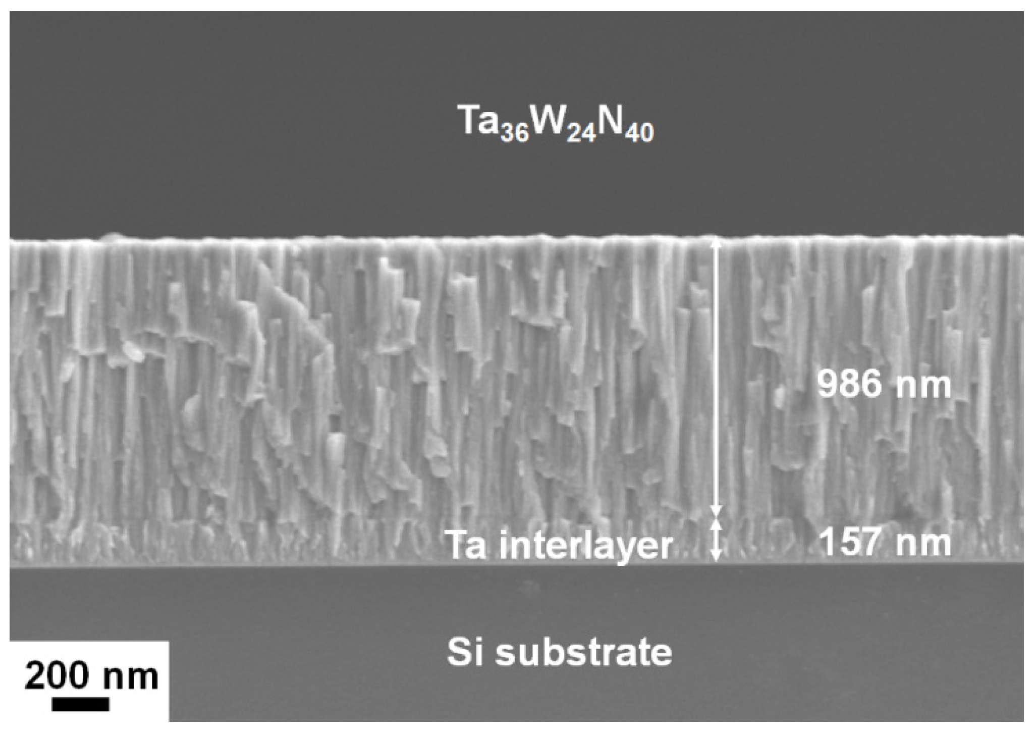
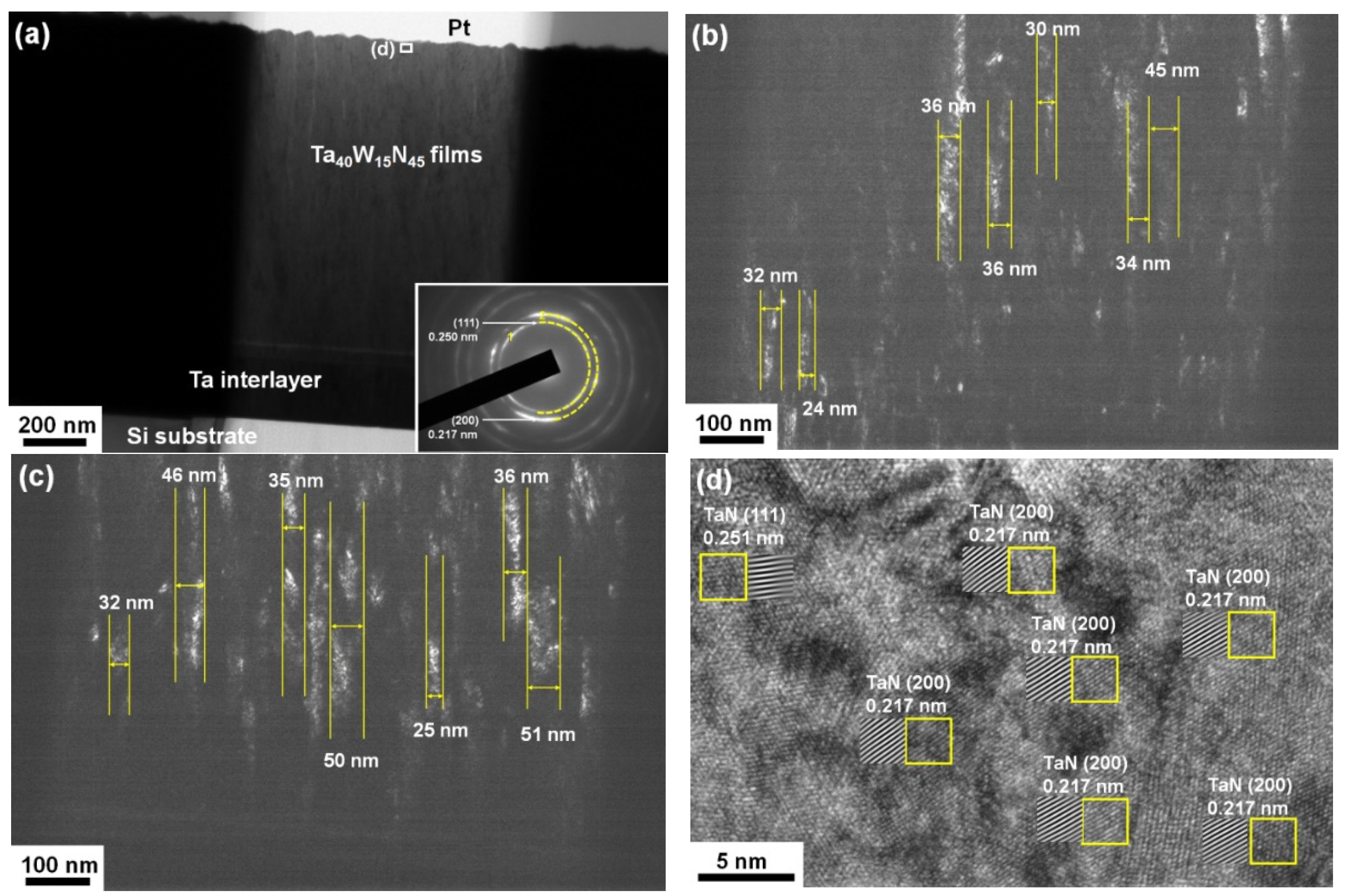
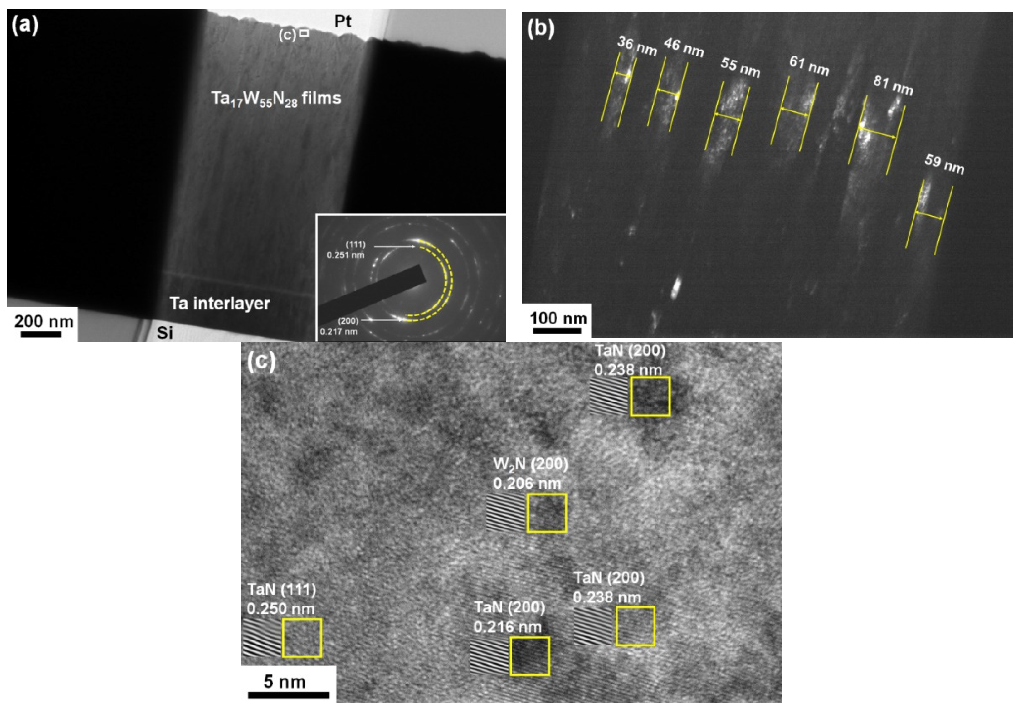
Figure 1 shows a typical cross-sectional SEM (XSEM) image of TaWN films with a columnar structure. Figure 2a displays the cross-sectional TEM (XTEM) image of the Ta40W15N45 sample with a Ta interlayer fabricated on a Si substrate. The inset in Figure 2a shows the selected area electron diffraction (SAED) pattern of the aforementioned sample, which indicates the existence of an fcc phase with evident (111), (200), (220) and (311) diffraction rings. The (111) and (200) diffraction rings had d-spacings of 0.250 and 0.217 nm, respectively, which are comparable with the standard values (0.2504 and 0.2169 nm) for the fcc TaN phase (ICDD 00-049-1283). Figure 2b,c depict the dark-field images corresponding to the (111) and (200) diffraction spots shown in Figure 2a, respectively. Columnar structures with widths of 24–45 and 25–51 nm existed in the aforementioned dark-field images, respectively. Lattice fringes of 0.251 and 0.217 nm corresponding to the (111) and (200) planes of the fcc TaN phase, respectively, were observed in the high-resolution TEM (HRTEM) image of the aforementioned sample (Figure 2d). The XTEM image and SAED pattern of the Ta17W55N28 sample (Figure 3a) were similar to those of the Ta40W15N45 sample. The dark-field image corresponding to the (111) diffraction spot of the Ta17W55N28 sample exhibited columnar widths of 36–81 nm (Figure 3b), which were larger than those of the Ta40W15N45 sample. The HRTEM image of the Ta17W55N28 film (Figure 3c) exhibited lattice fringes of TaN and W2N crystallites.
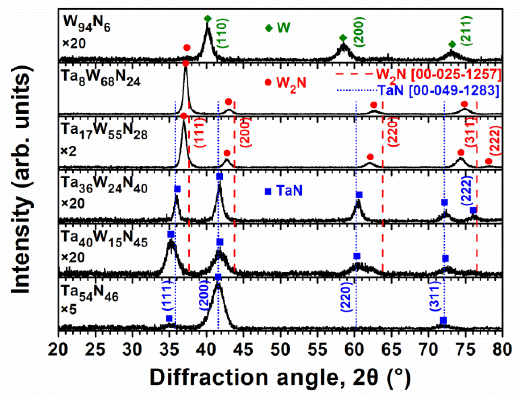
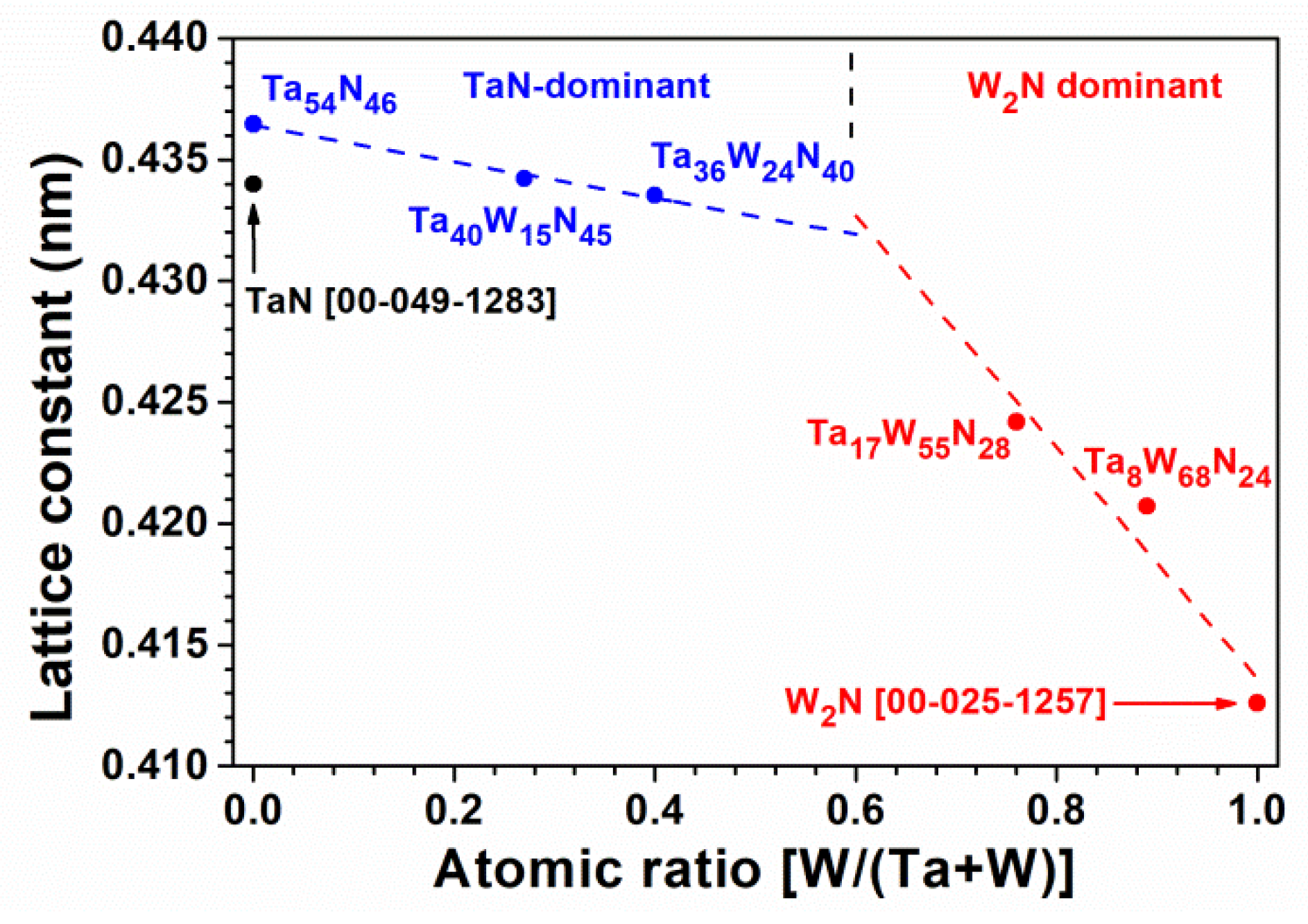
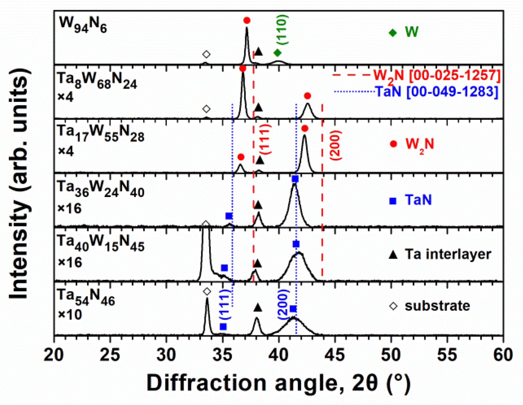
Figure 4 exhibits the grazing incident XRD (GIXRD) patterns of the TaWN films. The Ta54N46, Ta40W15N45, and Ta36W24N40 films exhibited an fcc phase with reflections close to the standard reflection angles of fcc TaN, whereas the reflections of the Ta17W55N28 and Ta8W68N24 films were located between the standard reflection angles of the TaN and W2N phases. The vertical lines in Figure 4 indicate the standard positions of reflections for TaN and W2N phases. Figure 5 illustrates the lattice constants of the TaWN films determined using (111), (200), (220), and (311) reflections in the GIXRD patterns. The standard lattice constant values of TaN (0.43399 nm) and W2N (0.41260 nm) are also shown for comparison. The atomic radii of Ta and W are 0.1430 and 0.1367 nm [43], respectively, which implies that substituting W atoms into the TaN lattice should decrease the lattice constant. The addition of W to the TaN lattice decreased the lattice constant from 0.4365 nm for the Ta54N46 film to 0.4342 and 0.4335 nm for the Ta40W15N45 and Ta36W24N40 films, respectively; then, the decrease in lattice constant became more evident, being reduced to 0.4242 and 0.4207 nm for the Ta17W55N28 and Ta8W68N24 films, respectively. Two linear fitting lines were obtained for the groups of (1) Ta54N46, Ta40W15N45, and Ta36W24N40 films and (2) Ta17W55N28 and Ta8W68N24 films and the standard W2N, respectively. The variation in the tendency to decrease with increasing W content implied the formation of solid solutions accompanied by the phase change from TaN-dominant to W2N-dominant structures. This observation is different from that reported by Yang et al. [26]. In their study [26], the lattice constant of W–Ta–N films linearly increased with increasing Ta content in the entire concentration range. The W94N6 films exhibited a body-centered cubic W phase with a lattice constant of 0.3160 nm determined from (110), (200), and (211) reflections. The standard lattice constant of cubic W is 0.31648 nm (ICDD 00-004-0806).
3.2. Chemical Bonding
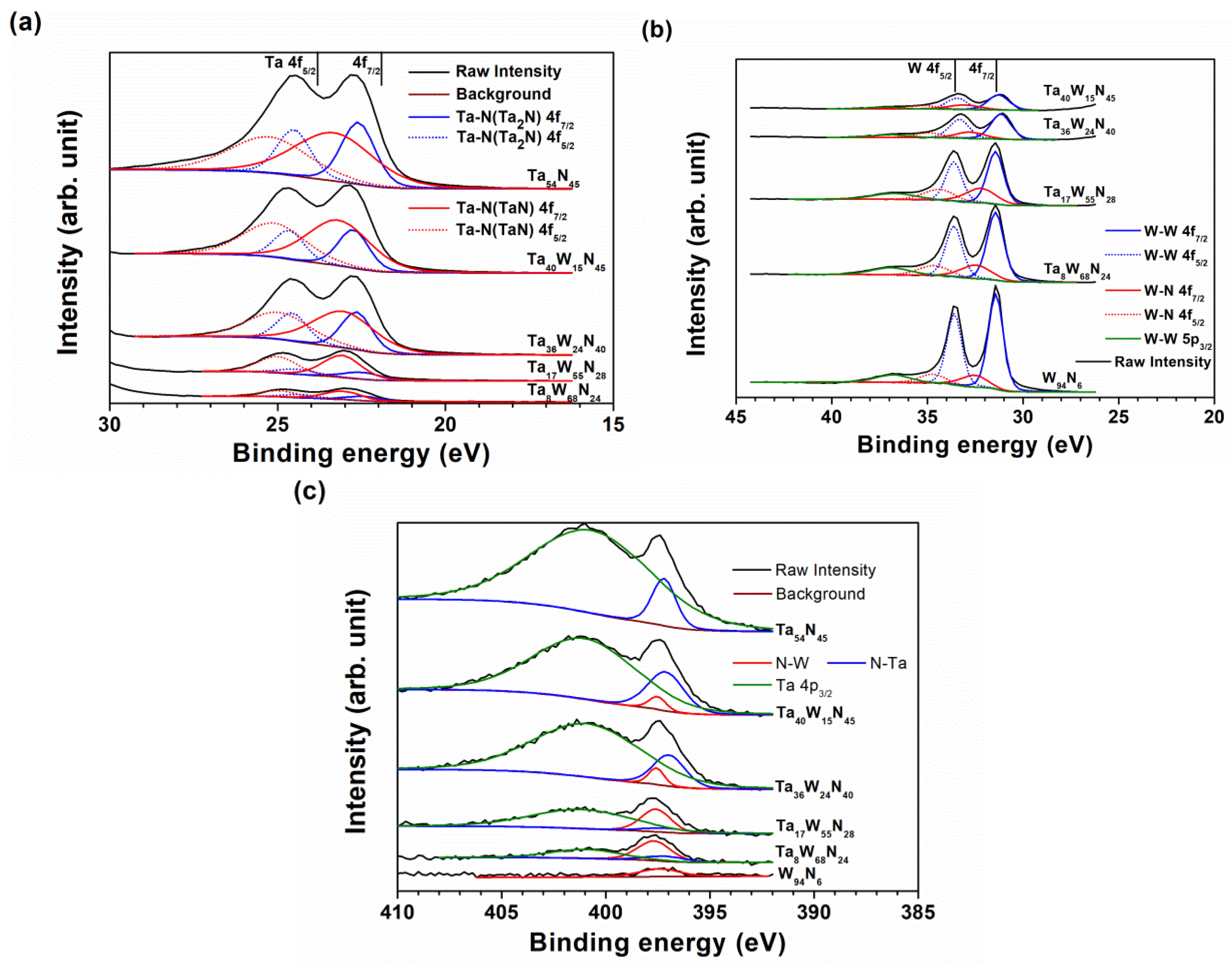
Figure 6 displays the XPS analyses of TaWN films at a depth of 49.8 nm. Ta 4f, W 4f, and N 1s signals were recorded. The aforementioned formation enthalpy for TaN and W2N at 298 K implied that TaN should have formed first, followed by W2N. Because all of the TaWN films were N-deficient, the Ta signals comprised two 4f doublets contributed by Ta–N bonds in Ta2N and TaN. The intensity ratios of Ta–N bonds of Ta2N to that of TaN (ITa2N:ITaN) were in the range of 24:76 to 33:67, as shown in Table 2. Table 2 lists the XPS analysis results obtained for the TaWN films at depths of 16.6, 24.9, 33.2, 41.5 and 49.8 nm. The binding energy values of Ta 4f7/2 for the Ta–N bonds in Ta2N and TaN compounds in the aforementioned TaWN films were 22.47–22.75 and 23.07–23.32 eV, respectively, which were comparable to the reported binding energies of Ta 4f7/2 of 22.3–22.9 eV [44,45,46,47] for Ta–N bonds in Ta2N and Ta 4f7/2 of 23.0–23.7 eV [44,45,46,47,48] for Ta–N bonds in TaN, respectively. The Ta 4f7/2 value for Ta–Ta bonds in pure Ta was 21.7–21.9 eV in the literature [44,45,47], which was not observed in this study. The 4f7/2 levels for pure Ta and W were 21.9 and 31.4 eV [37], respectively, and the standard values for 4f doublets were marked in Figure 6 for comparison. The W signals comprised W–W and W–N 4f doublets and a minor W–W 5p3/2 component and W–W bonds were the major forms of bonding. The intensity ratio IW–W:IW–N was higher than 68:32 for all the W-contained films. The low intensity of W–N bonds indicated the low affinity between W and N atoms. The binding energy values of W 4f7/2 for the W–W and W–N bonds in the fabricated TaWN films were 31.17–31.44 and 32.27–33.05 eV, respectively, which were comparable to the reported 31.2–31.7 eV for W films and 32.1–33.1 eV for W–N bonds [49,50,51,52]. The N 1s signals comprised N–Ta, N–W, and Ta 4p3/2 components. The N 1s signal of the Ta54N46 and W94N6 films was 397.44 and 397.71 eV, respectively. Moreover, the binding energy values of N–Ta and N–W bonds in the fabricated TaWN films were 397.27–397.41 and 397.83–397.95 eV, respectively, which implied that the N 1s binding energy levels of the N–W bonds were higher than those of the N–Ta bonds. Shen and Wang [53] reported that the binding energy values of N 1s were 396.9 and 397.9 eV in TaN and W2N, respectively. Greczynski et al. [54] reported 397.54 and 397.94 eV for the N 1s binding energy values of TaN and WN films, respectively. By contrast, Yang et al. [26] reported 397.3 and 398 eV for N–W and N–Ta binding energies, respectively.
3.3. Mechanical Properties
Table 3 lists the mechanical properties of the TaWN films. The average surface roughness values of TaWN films prepared on Si substrates were in the range of 1.6–2.7 nm, except for the W94N6 films, with a higher value of 4.7 nm, whereas the aforementioned films fabricated on the SUS420 plates revealed higher Ra values of 2.7–6.4 nm; however, all these Ra values were far below the radius of the probe tip used for nanoindentation testing. The Ta54N46 film exhibited a hardness (H) of 21.7 GPa and a Young’s modulus (E) of 277 GPa. The mechanical properties of the transition-metal nitride films were influenced by chemical stoichiometry, grain size, phase constitution, crystalline orientation, and residual stress caused by the formation technique. Various equilibrium and metastable phases of TaN films were studied [1]. In the present study, the TaWN films formed fcc solid solutions in which the lattice structures were TaN- or W2N-dominant depending on the chemical composition. With the addition of W to TaN, the hardness value increased from 21.7 GPa for the Ta54N46 film to 23.2, 24.5, 29.9, and 31.9 GPa for the Ta40W15N45, Ta36W24N40, Ta17W55N28 and Ta8W68N24 films, respectively, whereas the Young’s modulus value increased from 277 GPa for the Ta54N46 film to 302, 351, 381 and 391 GPa for the Ta40W15N45, Ta36W24N40, Ta17W55N28 and Ta8W68N24 films, respectively. By contrast, in [20], the hardness of TaZrN films decreased with increasing Zr content. The hardness decreased from 29.4 GPa for TaN0.86 film to 27.3, 26.3, 22.0 and 15.9 GPa for Ta0.95Zr0.05N0.97, Ta0.59Zr0.41N1.09, Ta0.28Zr0.72N1.05 and ZrN1.00 films, respectively [20]. The atomic radius of Zr is 0.16025 nm [43], which is larger than that of Ta (0.1430 nm) and W (0.1367 nm); therefore, the addition of Zr into the TaN matrix contributed a tensile stress component to the TaZrN solid solution, which resulted in variation in the residual stress from −3.46 GPa for TaN0.86 film to −2.62, −1.77, −0.01 and −0.11 GPa for the Ta0.95Zr0.05N0.97, Ta0.59Zr0.41N1.09, Ta0.28Zr0.72N1.05 and ZrN1.00 films [20]. The addition of W into the TaN matrix should increase the compressive stress level if the TaWN films formed a solid solution. However, all the TaWN films except for the Ta17W55N28 film exhibited a compressive residual stress level of 1.6–1.7 GPa. The Ta17W55N28 sample exhibited marginally high stress of −2.5 GPa; however, the hardness of the Ta17W55N28 sample (29.9 GPa) was lower than that of the Ta8W68N24 sample (31.9 GPa). The deviation in the hardness for the aforementioned TaWN films was not dominated by residual stress.
Yang et al. [26] and Xu et al. [27] reported that the hardness of TaWN films initially increased and then decreased with increasing W content. Yang et al. [26] observed a maximal hardness of 38 GPa for a Ta17W38N45 film because of the strengthening of the solid solution and the preferred (200) orientation, and Xu et al. [27] observed a maximal hardness of 32 GPa for a Ta41W17N42 film because of the strengthening of the solid solution and the phase change. Figure 7 displays the Bragg–Brentano XRD patterns of the TaWN films in this study. The reflections from the Ta interlayer and Si substrate were also observed. The TaN-dominant Ta54N46, Ta40W15N45 and Ta36W24N40 films exhibited high (200) intensities, whereas the W2N-dominant Ta17W55N28 and Ta8W68N24 films exhibited both (111) and (200) reflections. The grain sizes determined from the FWHM of (200) reflections in the Bragg–Brentano XRD patterns were 3.6, 3.7, 7.8, 15.6 and 12.0 nm for the Ta54N46, Ta40W15N45, Ta36W24N40, Ta17W55N28 and Ta8W68N24 films, respectively. The increase in the grain size of the aforementioned TaWN films was accompanied by an increase in hardness, which exhibited the inverse Hall–Petch relationship [55,56]. The Hall–Petch strengthening mechanism, which originated from the dislocation pile-up model, demonstrates the hardness enhancement with decreasing grain sizes for polycrystalline materials. Further decreasing the grain size to below a critical size such as 30 nm for nanocrystalline materials resulted in an inverse Hall–Petch behavior because of grain size softening effects, such as grain sliding or rotation. The critical grain size was reported to be 10, 12 and 10 nm for TaN [14], CrN [57] and TiZrN [58] films, respectively. In this study, the critical size was approximately 12 nm. The grain sizes of TaWN films reported in the works of Yang et al. [26] and Xu et al. [27] exhibited wider and higher ranges of 9–28 and 11–19 nm, respectively. The low intensity of the W(110) reflection in the Bragg–Brentano XRD pattern of the W94N6 films related to that shown in the GIXRD pattern was attributed to the effect of texture.
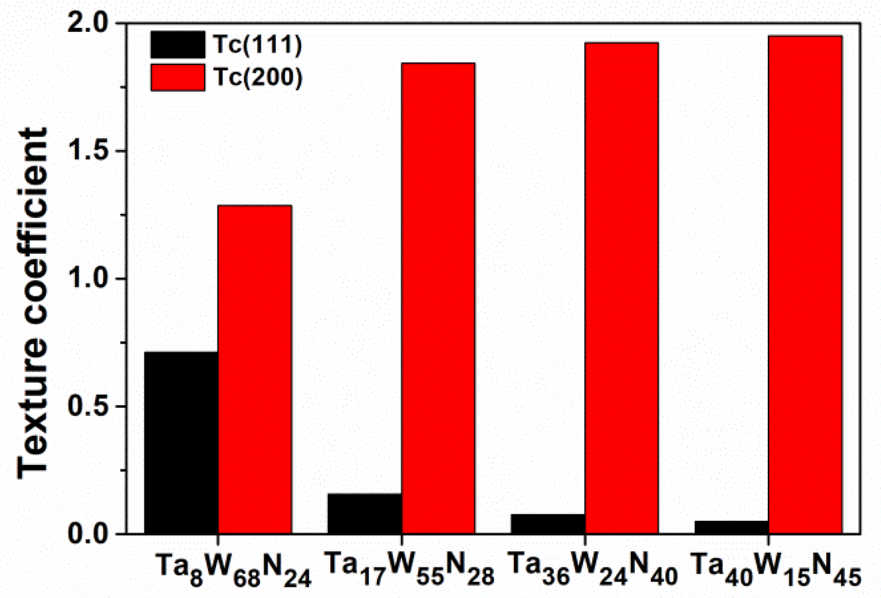
Figure 8 shows the texture coefficients of TaWN films, which indicates a (200) orientation for the reflections of all the TaWN films. The texture coefficients of the Ta40W15N45 and Ta36W24N40 films were determined using the standard value of 100:68 for the (111):(200) intensity ratio of the fcc TaN phase (ICDD 00-049-1283), whereas the texture coefficients of the Ta17W55N28 and Ta8W68N24 films were calculated using the standard value of 100:47 for the (111):(200) intensity ratio of the fcc W2N phase (ICDD 00-025-1257). The Tc(111):Tc(200) ratios exhibited similar levels of 0.05:1.95 and 0.08:1.92 for the Ta40W15N45 and Ta36W24N40 films, respectively, and changed to 0.16:1.84 and 0.71:1.29 for the W2N-dominant Ta17W55N28 and Ta8W68N24 films, respectively. The TaN film exhibited (200) texture because it possessed the lowest surface energy in a NaCl structure [59], whereas (111) planes were the closest packed in the fcc W2N structure with the lowest surface energy [60]. Therefore, the Tc (111) value increased with increasing W content in the TaWN films.
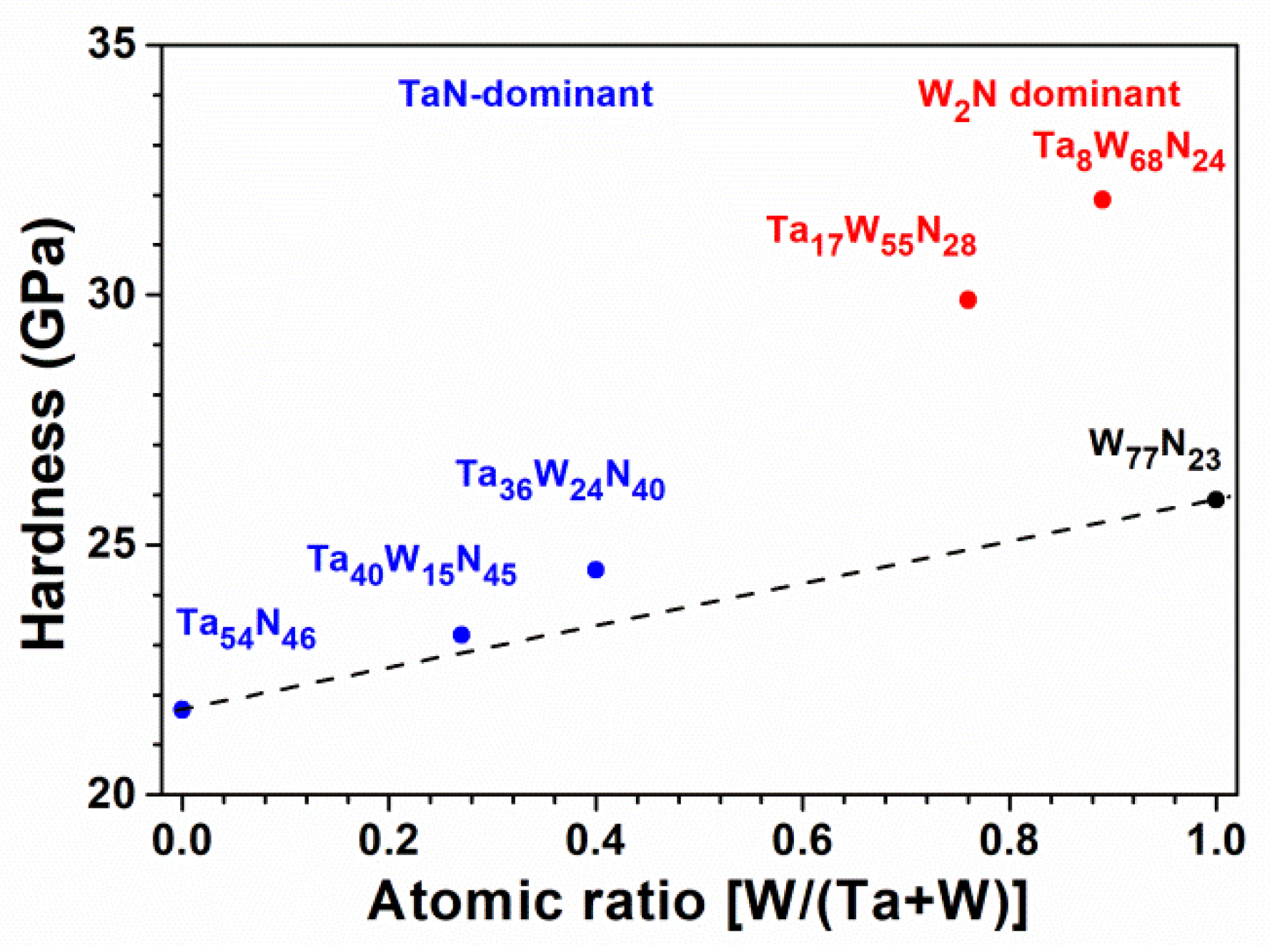
In a previous study [61], a W77N23 film that was prepared under a PW value of 150 W and a nitrogen flow ratio [N2/(N2 + Ar)] of 0.4 at room temperature exhibited a W2N phase, a residual stress of −1.6 GPa, a hardness of 25.9 GPa, and a Young’s modulus of 347 GPa. Under a stress level of −1.6 GPa, the hardness values of the Ta54N46 and W77N23 films were 21.7 and 25.9 GPa, respectively. Figure 9 depicts the relationship between the hardness values and atomic ratio (W/(Ta + W)) of the TaWN films. All TaWN films exhibited hardness levels above the line combining the hardness values of Ta54N46 and W77N23 films. This result implies that strengthening the solid solution and phase variation from TaN- to W2N-dominance are the main factors affecting the mechanical properties of TaWN films.
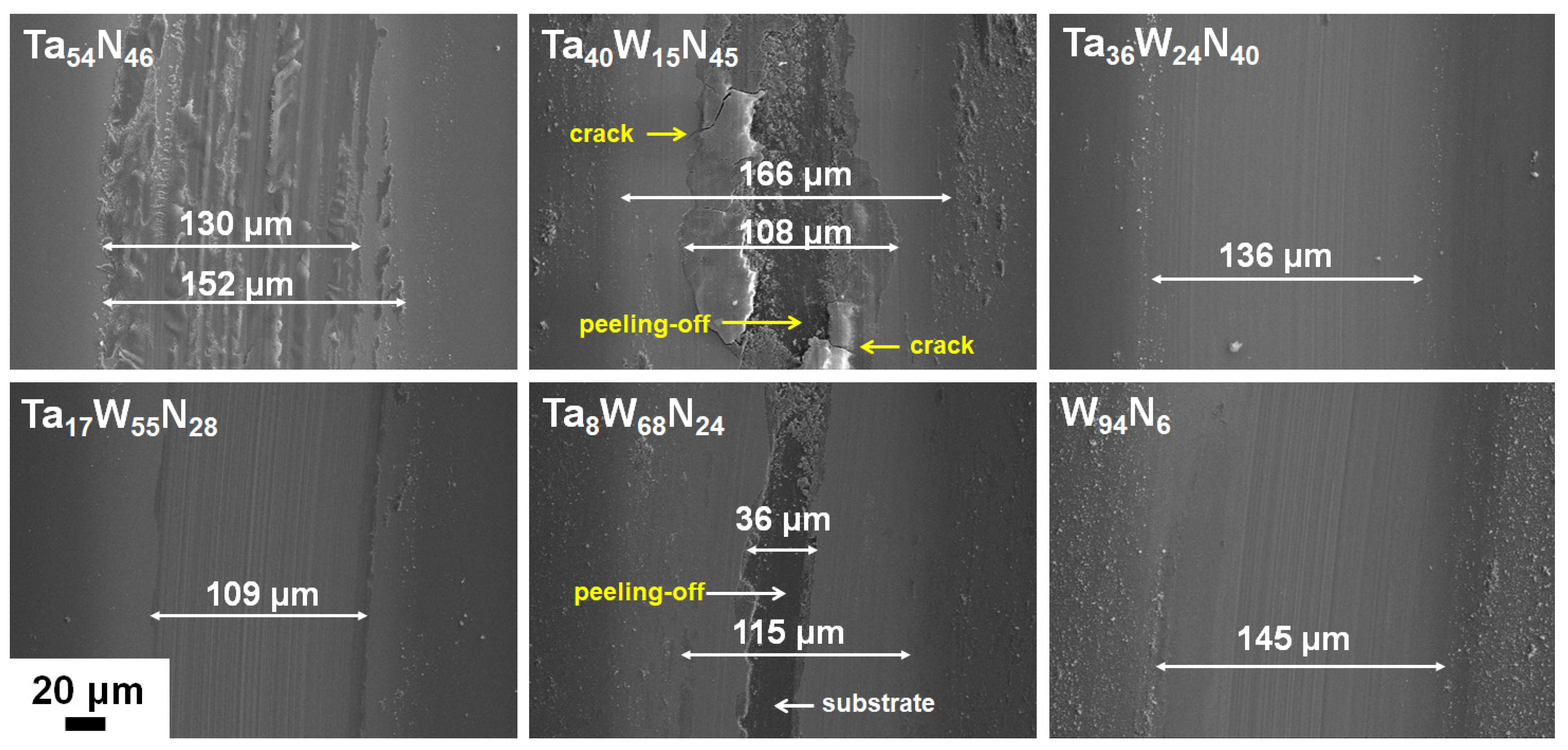
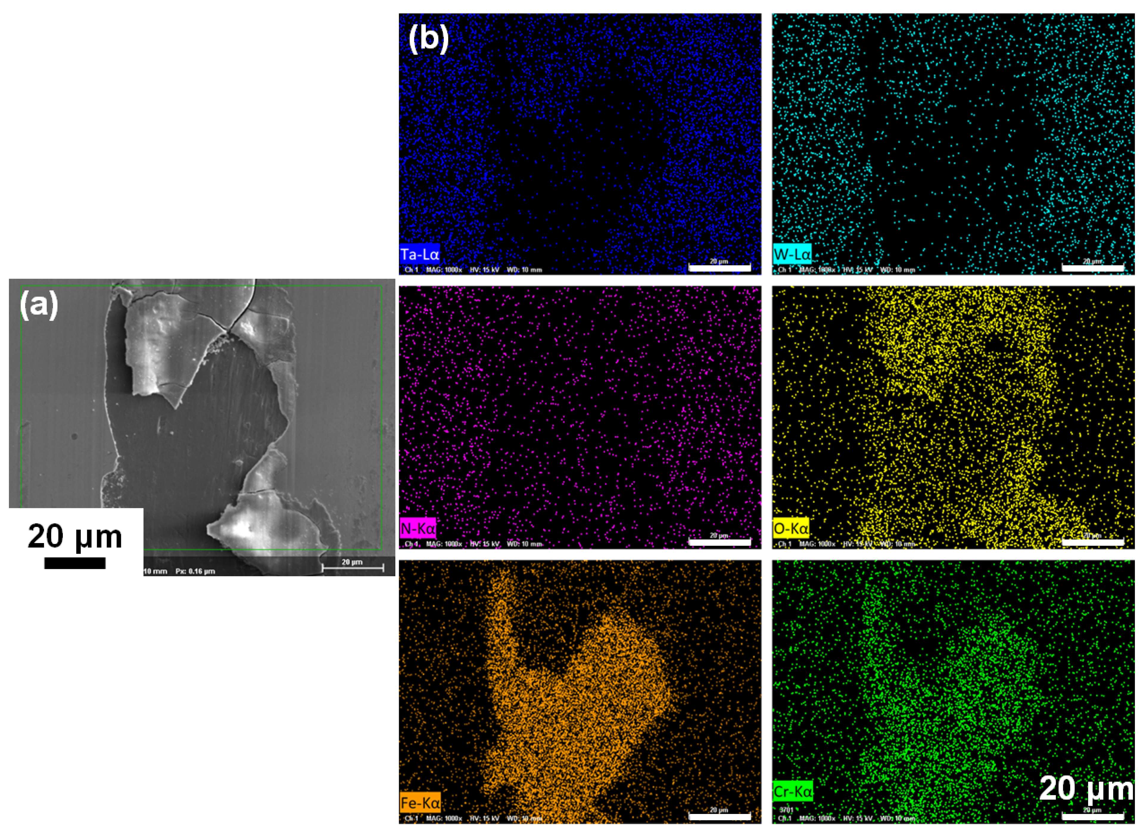
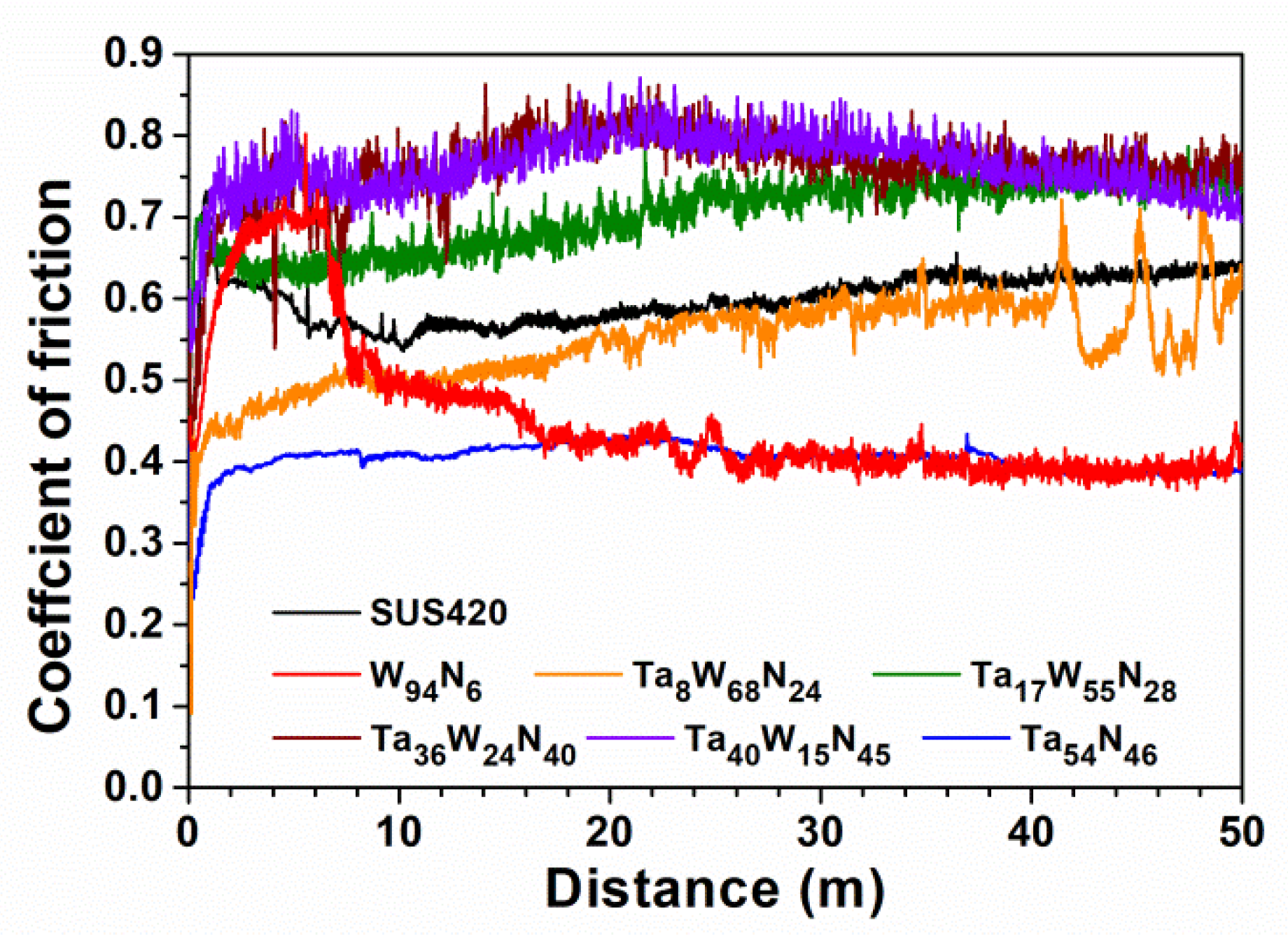
The indicators H/E, H/E* (E*: effective Young’s modulus), We (elastic recovery), and H3/E2 were used to evaluate the toughness and wear behavior of the fabricated films [62,63,64]. However, the use of H/E and H3/E2 to indicate the coating toughness of plastic materials was criticized [65]. In this study, the fcc TaWN films exhibited similar H/E values of 0.070–0.082, H/E* values of 0.062–0.074, and We values of 59–63% (Table 3), which implied that these films exhibited similar toughness. However, the H3/E2 values varied over a wide range, from 0.119 to 0.212 GPa (Table 3). Ta36W24N40 films exhibited the lowest levels of the aforementioned indicators within these fcc TaWN films. Figure 10 shows the wear scars of the TaWN/Ta/SUS420 samples against cemented tungsten carbide balls. The TaN-dominant Ta54N46, Ta40W15N45 and Ta36W24N40 films exhibited distinct morphologies after the wear test. The Ta54N46/Ta/SUS420 sample exhibited adhesive wear because of the chemical reaction on the contact area between the counterpart ball and films [59,66]. The wear debris attached to the films. The wear track width was 130–152 μm. The Ta40W15N45/Ta/SUS420 sample exhibited a wear track width of 166 μm. Crack propagation and peeling-off were observed in the inner part of the wear track. Figure 11 depicts the SEM image and elemental mappings of the Ta40W15N45/Ta/SUS420 sample, which exhibits an exposed substrate after the wear test. Fe and Cr signals attributed to the SUS420 substrate were observed at the interior of the wear track, whereas Ta, W, and N signals were absent. The peeling-off part of the Ta40W15N45 film revealed enriched Ta, W and O signals, but was N-deficient. The wear track of the Ta36W24N40/Ta/SUS420 sample was smooth and flat, which represented an abrasive wear behavior [66]. Table 4 lists the wear test results. The Ta54N46/Ta/SUS420 sample exhibited a wear depth of 682 nm, a coefficient of friction (COF) of 0.41, and a wear rate of 1.4 × 10⁻⁵ mm3/Nm. The addition of W into the TaN-dominant films increased the COFs to 0.77–0.78, whereas the wear rate was decreased to 8.3 and 7.6 × 10⁻⁶ mm3/Nm for the Ta40W15N45 and Ta36W24N40 samples, respectively. The W2N-dominant TaWN films, namely the Ta17W55N28 and Ta8W68N24 films, exhibited higher H3/E2 levels than those of the other films, which implied that the Ta8W68N24 film should have high wear resistance. However, the Ta8W68N24/Ta/SUS420 sample exhibited the most severe wear damage (Figure 10), with a wear depth of 1404 nm, which was greater than the sum of this sample’s film and interlayer thicknesses (1017 nm). Figure 12 displays the variations in the coefficient of friction (COF) values of the TaWN/Ta/SUS420 samples after sliding for 50 m. The Ta8W68N24/Ta/SUS420 sample exhibited abrupt deviations after sliding for 40 m. The low wear resistance of the Ta8W68N24/Ta/SUS420 sample could be attributed to the film’s texture, containing both (111) and (200) orientations. A TaN film with (111) texture was proposed to achieve adhesive wear behavior [59]. Samples with Ta36W24N40 and Ta17W55N28 top layers exhibited smooth wear scars, and their wear depths were smaller than their film thicknesses. The wear rates of the Ta36W24N40 and Ta17W55N28 samples were 7.6 and 4.9 × 10⁻⁶ mm3/Nm, respectively. The sample with a W94N6 top layer also exhibited a smooth wear scar and the lowest wear rate of 2.6 × 10⁻⁶ mm3/Nm because of its metallic W phase. The wear rate of the abrasive-wear-type samples decreased from 7.6 to 4.9 and 2.6 × 10⁻⁶ mm3/Nm as the COF value decreased from 0.77 to 0.74 and 0.40.
4. Conclusions
In this study, TaWN films with a Ta interlayer were fabricated using the direct current magnetron co-sputtering technique. The fabricated ternary TaWN films exhibited fcc solid solutions. Their structure changed from being TaN-dominant to being W2N-dominant when their W content was increased. Moreover, the chemical compositions of the aforementioned films exhibited sub-stoichiometric ratios in their fcc structures because of the low affinity between N and W atoms. The mechanical properties of the TaWN films improved when their W content was increased, which was attributed to the strengthening of the solid solution and the phase change from a TaN-dominant fcc to a W2N-dominant fcc. The Ta8W68N24 film exhibited the highest hardness (31.9 GPa) and Young’s modulus (391 GPa) as well as a low wear resistance in the pin-on-disk test. The Ta17W55N28 film exhibited the following acceptable mechanical properties: a hardness of 29.9 GPa, a Young’s modulus of 381 GPa, and a low wear rate of 4.9 × 10⁻⁶ mm3/Nm.
Author Contributions
Conceptualization, L.-C.C. and Y.-I.C.; Funding acquisition, L.-C.C. and Y.-I.C.; Investigation, C.-H.T.; Resources, L.-C.C. and Y.-I.C.; Validation, L.-C.C.; Visualization, C.-H.T.; Writing—original draft, C.-H.T.; Writing—review and editing, Y.-I.C. All authors have read and agreed to the published version of the manuscript.
Funding
This research was funded by the Ministry of Science and Technology, Taiwan, grant numbers 110-2221-E-019-015 and 110-2221-E-131-013. The APC was funded by the National Taiwan Ocean University.
Institutional Review Board Statement
Not applicable.
Informed Consent Statement
Not applicable.
Data Availability Statement
Not applicable.
Acknowledgments
The authors thank the Instrumentation Center at the National Tsing Hua University for EPMA and XPS analyses (MOST 110-2731-M-007-001, EPMA000200 and ESCA000300). Thanks are also given to the Joint Center for High Valued Instruments at NSYSU for the FIB (EM025100) operation.
Conflicts of Interest
The authors declare no conflict of interest.
References
- Shin, C.S.; Kim, Y.W.; Gall, D.; Greene, J.E.; Petrov, I. Phase composition and microstructure of polycrystalline and epitaxial TaNxlayers grown on oxidized Si(001) and MgO(001) by reactive magnetron sputter deposition. Thin Solid Films 2002, 402, 172–182. [Google Scholar] [CrossRef]
- Li, H.; Li, J.; Yan, C.; Huang, J.; Kong, J.; Wu, Q.; Shi, Y.; Xiong, D. Deposition and mechanical properties of δ-TaNx films with different stoichiometry by DC magnetron sputtering. Surf. Coat. Technol. 2020, 404, 126452. [Google Scholar] [CrossRef]
- Baker, C.C.; Shah, S.I. Reactive sputter deposition of tungsten nitride thin films. J. Vac. Sci. Technol. A 2002, 20, 1699–1703. [Google Scholar] [CrossRef]
- Lou, B.S.; Moirangthem, I.; Lee, J.W. Fabrication of tungsten nitride thin films by superimposed HiPIMS and MF system: Effects of nitrogen flow rate. Surf. Coat. Technol. 2020, 393, 125743. [Google Scholar] [CrossRef]
- Inspektor, A.; Salvador, P.A. Architecture of PVD coatings for metalcutting applications: A review. Surf. Coat. Technol. 2014, 257, 138–153. [Google Scholar] [CrossRef]
- Nordin, M.; Ericson, F. Growth characteristics of multilayered physical vapour deposited TiN/TaNx on high speed steel substrate. Thin Solid Films 2001, 385, 174–181. [Google Scholar] [CrossRef]
- Chen, Y.I.; Lin, B.L.; Kuo, Y.C.; Huang, J.C.; Chang, L.C.; Lin, Y.T. Preparation and annealing study of TaNx coatings on WC-Co substrates. Appl. Surf. Sci. 2011, 257, 6741–6749. [Google Scholar] [CrossRef]
- Riekkinen, T.; Molarius, J.; Laurila, T.; Nurmela, A.; Suni, I.; Kivilahti, J.K. Reactive sputter deposition and properties of TaxN thin films. Microelectron. Eng. 2002, 64, 289–297. [Google Scholar] [CrossRef]
- Dalili, N.; Liu, Q.; Ivey, D.G. Thermal and electrical stability of TaNx diffusion barriers for Cu metallization. J. Mater. Sci. 2013, 48, 489–501. [Google Scholar] [CrossRef]
- Leng, Y.X.; Sun, H.; Yang, P.; Chen, J.Y.; Wang, J.; Wan, G.J.; Huang, N.; Tian, X.B.; Wang, L.P.; Chu, P.K. Biomedical properties of tantalum nitride films synthesized by reactive magnetron sputtering. Thin Solid Films 2001, 398–399, 471–475. [Google Scholar] [CrossRef]
- Jiang, P.C.; Chen, J.S.; Lin, Y.K. Structural and electrical characteristics of W–N thin films prepared by reactive rf sputtering. J. Vac. Sci. Technol. A 2003, 21, 616–622. [Google Scholar] [CrossRef]
- Lee, G.R.; Lee, J.J.; Shin, C.S.; Petrov, I.; Greene, J.E. Self-organized lamellar structured tantalum–nitride by UHV unbalanced-magnetron sputtering. Thin Solid Films 2005, 475, 45–48. [Google Scholar] [CrossRef]
- Li, T.C.; Lwo, B.J.; Pu, N.W.; Yu, S.P.; Kao, C.H. The effects of nitrogen partial pressure on the properties of the TaNx films deposited by reactive magnetron sputtering. Surf. Coat. Technol. 2006, 201, 1031–1036. [Google Scholar] [CrossRef]
- Bernoulli, D.; Müller, U.; Schwarzenberger, M.; Hauert, R.; Spolenak, R. Magnetron sputter deposited tantalum and tantalum nitride thin films: An analysis of phase, hardness and composition. Thin Solid Films 2013, 548, 157–161. [Google Scholar] [CrossRef]
- Yang, Y.H.; Chen, D.J.; Wu, F.B. Microstructure, hardness, and wear resistance of sputtering TaN coating by controlling RF input power. Surf. Coat. Technol. 2016, 303, 32–40. [Google Scholar] [CrossRef]
- Chim, Y.C.; Ding, X.Z.; Zeng, X.T.; Zhang, S. Oxidation resistance of TiN, CrN, TiAlN and CrAlN coatings deposited by lateral rotating cathode arc. Thin Solid Films 2009, 517, 4845–4849. [Google Scholar] [CrossRef]
- Tang, J.F.; Lin, C.Y.; Yang, F.C.; Chang, C.L. Influence of nitrogen content and bias voltage on residual stress and the tribological and mechanical properties of CrAlN films. Coatings 2020, 10, 546. [Google Scholar] [CrossRef]
- Lin, C.H.; Duh, J.G.; Yau, B.S. Processing of chromium tungsten nitride hard coatings for glass molding. Surf. Coat. Technol. 2006, 201, 1316–1322. [Google Scholar] [CrossRef]
- Huang, A.; Xie, Z.; Li, K.; Chen, Q.; Chen, Y.; Gong, F. Thermal stability of CrWN glass molding coatings after vacuum annealing. Coatings 2020, 10, 198. [Google Scholar] [CrossRef] [Green Version]
- Chang, L.C.; Chang, C.Y.; Chen, Y.I. Mechanical properties and oxidation resistance of reactively sputtered Ta1−xZrxNy thin films. Surf. Coat. Technol. 2015, 280, 27–36. [Google Scholar] [CrossRef]
- Wei, C.T.; Shieh, H.P.D. Effects of processing variables on tantalum nitride by reactive-ion-assisted magnetron sputtering deposition. Jpn. J. Appl. Phys. 2006, 45, 6405–6410. [Google Scholar] [CrossRef]
- Hones, P.; Sanjinés, R.; Lévy, F. Sputter deposited chromium nitride based ternary compounds for hard coatings. Thin Solid Films 1998, 332, 240–246. [Google Scholar] [CrossRef]
- Čekada, M.; Panjan, P.; Navinšek, B.; Cvelbar, F. Characterization of (Cr,Ta)N hard coatings reactively sputtered at low temperature. Vacuum 1999, 52, 461–467. [Google Scholar] [CrossRef]
- Zhao, X.; Li, H.; Li, J.; Hu, J.; Huang, J.; Kong, J.; Wu, Q.; Shi, Y.; Xiong, D. Mechanical and tribological behaviors of hard and tough TaxHf1−xN films with various Ta contents. Surf. Coat. Technol. 2020, 403, 126412. [Google Scholar] [CrossRef]
- Xu, J.; Xue, Y.; Cao, J.; Yu, L. Microstructures, Mechanical and Friction Properties of TaMoN Composite Films. Rare Metal Mater. Eng. 2014, 43, 1412–1416. [Google Scholar]
- Yang, J.F.; Jiang, Y.; Yuan, Z.G.; Wang, X.P.; Fang, Q.F. Manufacture, microstructure and mechanical properties of W–Ta–N nano-structured hard films. Appl. Surf. Sci. 2012, 258, 7849–7854. [Google Scholar] [CrossRef]
- Xu, J.; Luo, H.; Ju, H.; Yu, L.; Zhou, G. Microstructure, mechanical and tribological properties of TaWN composite films. Vacuum 2017, 146, 246–251. [Google Scholar] [CrossRef]
- Liu, Y.; Song, S.; Mao, D.; Ling, H.; Li, M. Diffusion barrier performance of reactively sputtered Ta–W–N between Cu and Si. Microelectron. Eng. 2004, 75, 309–315. [Google Scholar] [CrossRef]
- Takeyama, M.B.; Sato, M.; Yasuda, M. Relationship between 〈111〉-oriented Cu film and thin Ta–W–N barrier. Jpn. J. Appl. Phys. 2020, 59, SLLD02. [Google Scholar] [CrossRef]
- Chang, L.C.; Zheng, Y.Z.; Gao, Y.X.; Chen, Y.I. Mechanical properties and oxidation resistance of sputtered Cr–W–N coatings. Surf. Coat. Technol. 2017, 320, 196–200. [Google Scholar] [CrossRef]
- Yang, J.F.; Yuan, Z.G.; Wang, X.P.; Fang, Q.F. Characterization of W–Ta–N hard films synthesized by direct current magnetron sputtering. Surf. Coat. Technol. 2013, 231, 19–23. [Google Scholar] [CrossRef]
- Chen, Y.I.; Lin, K.Y.; Wang, H.H.; Cheng, Y.R. Characterization of Ta–Si–N coatings prepared using direct current magnetron co-sputtering. Appl. Surf. Sci. 2014, 305, 805–816. [Google Scholar] [CrossRef]
- Tong, C.Y.; Lee, J.W.; Kuo, C.C.; Huang, S.H.; Chan, Y.C.; Chen, H.W.; Duh, J.G. Effects of carbon content on the microstructure and mechanical property of cathodic arc evaporation deposited CrCN thin films. Surf. Coat. Technol. 2013, 231, 482–486. [Google Scholar] [CrossRef]
- Cullity, B.D.; Stock, S.R. Elements of X-ray Diffraction, 3rd ed.; Prentice-Hall: Hoboken, NJ, USA, 2001; pp. 169–170. [Google Scholar]
- Greczynski, G.; Hultman, L. C1s peak of adventitious carbon aligns to the vacuum level: Dire consequences for material’s bonding assignment by photoelectron spectroscopy. Chem. Phys. Chem. 2017, 18, 1507–1512. [Google Scholar] [CrossRef]
- Greczynski, G.; Hultman, L. Reliable determination of chemical state in X-ray photoelectron spectroscopy based on sample-work-function referencing to adventitious carbon: Resolving the myth of apparent constant binding energy of the C 1s peak. Appl. Surf. Sci. 2018, 451, 99–103. [Google Scholar] [CrossRef]
- Moulder, J.F.; Stickle, W.F.; Sobol, P.E.; Bomben, K.D. Handbook of X-ray Photoelectron Spectroscopy; Chastain, J., King, R.C., Eds.; Physical Electronics: Chanhassen, MN, USA, 1995. [Google Scholar]
- Oliver, W.C.; Pharr, G.M. An improved technique for determining hardness and elastic modulus using load and displacement sensing indentation experiments. J. Mater. Res. 1992, 7, 1564–1583. [Google Scholar] [CrossRef]
- Janssen, G.C.A.M.; Abdalla, M.M.; van Keulen, F.; Pujada, B.R.; van Venrooy, B. Celebrating the 100th anniversary of the Stoney equation for film stress: Developments from polycrystalline steel strips to single crystal silicon wafers. Thin Solid Films 2009, 517, 1858–1867. [Google Scholar] [CrossRef]
- Thod, L.E. Transition Metal Carbides and Nitrides; Academic Press: New York, NY, USA, 1971. [Google Scholar]
- Barin, I. Thermochemical Data of Pure Substances, 3rd ed.; VCH: New York, NY, USA, 1995. [Google Scholar]
- de Boer, F.R.; Boom, R.; Mattens, W.C.M.; Miedema, A.R.; Niessen, A.K. Transition Metal Alloys; North-Holland: Amsterdam, The Netherlands, 1988. [Google Scholar]
- Senkov, O.N.; Miracle, D.B. Effect of the atomic size distribution on glass forming ability of amorphous metallic alloys. Mater. Res. Bull. 2001, 36, 2183–2198. [Google Scholar] [CrossRef]
- Chang, C.C.; Jeng, J.S.; Chen, J.S. Microstructural and electrical characteristics of reactively sputtered Ta-N thin films. Thin Solid Films 2002, 413, 46–51. [Google Scholar] [CrossRef]
- Arranz, A.; Palacio, C. Composition of tantalum nitride thin films grown by low-energy nitrogen implantation: A factor analysis study of the Ta 4 f XPS core level. Appl. Phys. A 2005, 81, 1405–1410. [Google Scholar] [CrossRef] [Green Version]
- Scandurra, A.; Indelli, G.F.; Pignataro, B.; Di Marco, S.; Di Stefano, M.A.; Ravesi, S.; Pignataro, S. Tantalum nitride thin film resistors by low temperature reactive sputtering for plastic electronics. Surf. Interface Anal. 2008, 40, 758–762. [Google Scholar] [CrossRef]
- Arshi, N.; Lu, J.; Joo, Y.K.; Yoon, J.H.; Koo, B.H. Effects of nitrogen composition on the resistivity of reactively sputtered TaN thin films. Surf. Interface Anal. 2015, 47, 154–160. [Google Scholar] [CrossRef]
- Zaman, A.; Meletis, E.I. Microstructure and mechanical properties of TaN thin films prepared by reactive magnetron sputtering. Coatings 2017, 7, 209. [Google Scholar] [CrossRef] [Green Version]
- Wen, M.; Meng, Q.N.; Yu, W.X.; Zheng, W.T.; Mao, S.X.; Hua, M.J. Growth, stress and hardness of reactively sputtered tungsten nitride thin films. Surf. Coat. Technol. 2010, 205, 1953–1961. [Google Scholar] [CrossRef]
- Fu, T.; Shen, Y.G.; Zhou, Z.F.; Li, K.Y. Thermal stability of sputter deposited nanocrystalline W2N/amorphous Si3N4 coatings. J. Vac. Sci. Technol. A 2006, 24, 2094–2099. [Google Scholar] [CrossRef]
- Louro, C.; Cavaleiro, A.; Montemor, F. How is the chemical bonding of W–Si–N sputtered coatings? Surf. Coat. Technol. 2001, 142–144, 964–970. [Google Scholar] [CrossRef]
- Liu, Y.H.; Chang, L.C.; Liu, B.W.; Chen, Y.I. Mechanical properties and oxidation behavior of W–Si–N coatings. Surf. Coat. Technol. 2019, 375, 727–738. [Google Scholar] [CrossRef]
- Shen, L.; Wang, N. Effect of nitrogen pressure on the structure of Cr-N, Ta-N, Mo-N, and W-N nanocrystals synthesized by arc discharge. J. Nanomater. 2011, 2011, 781935. [Google Scholar] [CrossRef]
- Greczynski, G.; Primetzhofer, D.; Lu, J.; Hultman, L. Core-level spectra and binding energies of transition metal nitrides by non-destructive X-ray photoelectron spectroscopy through capping layers. Appl. Surf. Sci. 2017, 396, 347–358. [Google Scholar] [CrossRef] [Green Version]
- Naik, S.N.; Walley, S.M. The Hall–Petch and inverse Hall–Petch relations and the hardness of nanocrystalline metals. J. Mater. Sci. 2020, 55, 2661–2681. [Google Scholar] [CrossRef] [Green Version]
- Quek, S.S.; Chooi, Z.H.; Wu, Z.; Zhang, Y.W.; Srolovitz, D.J. The inverse hall–petch relation in nanocrystalline metals: A discrete dislocation dynamics analysis. J. Mech. Phys. Solids 2016, 88, 252–266. [Google Scholar] [CrossRef]
- Mayrhofer, P.H.; Tischler, G.; Mitterer, C. Microstructure and mechanical/thermal properties of Cr–N coatings deposited by reactive unbalanced magnetron sputtering. Surf. Coat. Technol. 2001, 142–144, 78–84. [Google Scholar] [CrossRef]
- Escobar, D.; Ospina, R.; Gómez, A.G.; Restrepo-Parra, E. Microstructure, residual stress and hardness study of nanocrystalline titanium–zirconium nitride thin films. Ceram. Int. 2015, 41, 947–952. [Google Scholar] [CrossRef]
- Tan, P.; Fu, L.; Teng, J.; Zhu, J.; Yang, W.; Li, D.; Zhou, L. Effect of texture on wear resistance of tantalum nitride film. Tribo. Int. 2019, 133, 126–135. [Google Scholar] [CrossRef]
- Addonizio, M.L.; Castaldo, A.; Antonaia, A.; Gambale, E.; Iemmo, L. Influence of process parameters on properties of reactively sputtered tungsten nitride thin films. J. Vac. Sci. Technol. A 2012, 30, 031506. [Google Scholar] [CrossRef]
- Chang, L.C.; Sung, M.C.; Chu, L.H.; Chen, Y.I. Effects of the nitrogen flow ratio and substrate bias on the mechanical properties of W–N and W–Si–N Films. Coatings 2020, 10, 1252. [Google Scholar] [CrossRef]
- Pogrebnjak, A.D.; Beresnev, V.M.; Bondar, O.V.; Postolnyi, B.O.; Zaleski, K.; Coy, E.; Jurga, S.; Lisovenko, M.O.; Konarski, P.; Rebouta, L.; et al. Superhard CrN/MoN coatings with multilayer architecture. Mater. Des. 2018, 153, 47–59. [Google Scholar] [CrossRef]
- Musil, J. Hard nanocomposite coatings: Thermal stability, oxidation resistance and toughness. Surf. Coat. Technol. 2012, 207, 50–65. [Google Scholar] [CrossRef]
- Tsui, T.Y.; Pharr, G.M.; Oliver, W.C.; Bhatia, C.S.; White, R.L.; Anders, S.; Anders, A.; Brown, I.G. Nanoindentation and nanoscratching of hard carbon coatings for magnetic disks. Mater. Res. Soc. Symp. Proc. 1995, 383, 447–452. [Google Scholar] [CrossRef] [Green Version]
- Chen, X.; Du, Y.; Chung, Y.W. Commentary on using H/E and H3/E2 as proxies for fracture toughness of hard coatings. Thin Solid Films 2019, 688, 137265. [Google Scholar] [CrossRef]
- Kim, D.J.; La, J.H.; Kim, K.S.; Kim, S.M.; Lee, S.Y. Tribological properties of CrZr–Si–N films synthesized using Cr–Zr–Si segment targets. Surf. Coat. Technol. 2014, 259, 71–76. [Google Scholar] [CrossRef]
Figure 1.
XSEM image of the Ta36W24N40 film prepared on a Si substrate.

Figure 2.
(a) XTEM image and SAED pattern, dark-field images corresponding to the (b) (111) and (c) (200) spots in SAED pattern and (d) HRTEM image of the Ta40W15N45 film.
Figure 2.
(a) XTEM image and SAED pattern, dark-field images corresponding to the (b) (111) and (c) (200) spots in SAED pattern and (d) HRTEM image of the Ta40W15N45 film.

Figure 3.
(a) XTEM image and SAED pattern, (b) dark-field image corresponding to the (200) spot in the SAED pattern, and (c) HRTEM image of the Ta17W55N28 film.
Figure 3.
(a) XTEM image and SAED pattern, (b) dark-field image corresponding to the (200) spot in the SAED pattern, and (c) HRTEM image of the Ta17W55N28 film.

Figure 4.
GIXRD patterns of the TaWN films. (Vertical lines indicate the standard positions of reflections for TaN (ICDD 00-049-1283) and W2N (ICDD 00-025-1257), respectively).
Figure 4.
GIXRD patterns of the TaWN films. (Vertical lines indicate the standard positions of reflections for TaN (ICDD 00-049-1283) and W2N (ICDD 00-025-1257), respectively).

Figure 5.
Lattice constants of the TaWN films.

Figure 6.
(a) Ta, (b) W, and (c) N signals at a depth of 49.8 nm for the TaWN films.

Figure 7.
Bragg–Brentano XRD patterns of the TaWN films.

Figure 8.
Texture coefficients of the TaWN films.

Figure 9.
Hardness values of the TaWN films.

Figure 10.
Wear scars of the TaWN/Ta/SUS420 samples after sliding for 50 m.

Figure 11.
(a) SEM image and (b) elemental mappings of the Ta40W15N45 film after the wear test.

Figure 12.
COFs of the TaWN/Ta/SUS420 samples.


Table 1.
Sputtering parameters, chemical compositions, and thicknesses of the TaWN films.
| Sample | Power (W) | Chemical Composition (at.%) | N/M1 | T2 | I3 | R4 | ||||
|---|---|---|---|---|---|---|---|---|---|---|
| PTa | PW | Ta | W | N | O | (nm) | (nm) | (nm/min) | ||
| Ta54N46 | 250 | 0 | 52.9 ± 0.7 | - | 44.8 ± 1.1 | 2.3 ± 0.7 | 0.85 | 894 | 170 | 8.9 |
| Ta40W15N45 | 250 | 50 | 39.3 ± 3.7 | 14.9 ± 0.9 | 45.1 ± 3.2 | 0.7 ± 1.2 | 0.83 | 813 | 152 | 12.5 |
| Ta36W24N40 | 200 | 100 | 35.7 ± 0.4 | 23.2 ± 0.8 | 39.5 ± 0.6 | 1.6 ± 0.0 | 0.67 | 986 | 157 | 15.2 |
| Ta17W55N28 | 100 | 200 | 16.6 ± 0.0 | 54.4 ± 0.0 | 27.4 ± 0.0 | 1.6 ± 0.0 | 0.39 | 939 | 157 | 14.4 |
| Ta8W68N24 | 50 | 250 | 7.5 ± 0.0 | 67.0 ± 0.0 | 24.0 ± 0.0 | 1.5 ± 0.0 | 0.32 | 885 | 132 | 13.6 |
| W94N6 | 0 | 250 | - | 87.9 ± 0.6 | 5.8 ± 0.3 | 6.3 ± 0.4 | 0.06 | 1203 | 130 | 12.0 |
1 N/M: atomic ratio of N to the sum of metal atoms; 2 T: film thickness; 3 I: Ta interlayer thickness; 4 R: Deposition rate of TaWN film.
Table 2.
XPS analysis results for the TaWN films at depths of 16.6–49.8 nm.
| Sample | Ta 4f7/2 (eV) | ITa2N:ITaN 1 | W 4f7/2 (eV) | IW–W:IW–N 2 | N 1s (eV) | IN–Ta:IN–W 3 | |||
|---|---|---|---|---|---|---|---|---|---|
| (Ta–N)Ta2N | (Ta–N)TaN | W–W | W–N | N–Ta | N–W | ||||
| Ta54N46 | 22.60 ± 0.01 | 23.32 ± 0.01 | 33:67 | - | - | - | 397.44 ± 0.01 | - | 100:0 |
| Ta40W15N45 | 22.75 ± 0.01 | 23.22 ± 0.02 | 28:72 | 31.29 ± 0.02 | 33.05 ± 0.06 | 68:32 | 397.31 ± 0.04 | 397.85 ± 0.05 | 80:20 |
| Ta36W24N40 | 22.66 ± 0.01 | 23.07 ± 0.02 | 32:68 | 31.17 ± 0.02 | 32.76 ± 0.13 | 73:27 | 397.27 ± 0.04 | 397.83 ± 0.06 | 82:18 |
| Ta17W55N28 | 22.52 ± 0.04 | 23.10 ± 0.01 | 24:76 | 31.44 ± 0.00 | 32.27 ± 0.07 | 68:32 | 397.33 ± 0.05 | 397.87 ± 0.02 | 26:74 |
| Ta8W68N24 | 22.47 ± 0.04 | 23.07 ± 0.02 | 30:70 | 31.43 ± 0.01 | 32.40 ± 0.13 | 72:28 | 397.41 ± 0.04 | 397.95 ± 0.03 | 26:74 |
| W94N6 | - | - | - | 31.43 ± 0.01 | 32.58 ± 0.03 | 82:18 | - | 397.71 ± 0.13 | 0:100 |
1 ITa2N:ITaN: intensity ratio of Ta–N bonds in the Ta2N phase to those in the TaN phase; 2,3 IX–Y: intensity of X–Y bonds.
Table 3.
Mechanical properties of the TaWN/Ta/Si samples.
| Sample | H1 | E2 | H/E | H/E*3 | H3/E2 | We4 | σ5 | Ra6 |
|---|---|---|---|---|---|---|---|---|
| (GPa) | (GPa) | (%) | (GPa) | (nm) | ||||
| Ta54N46 | 21.7 ± 2.5 | 277 ± 22 | 0.078 | 0.069 | 0.133 | 59 | −1.6 ± 0.1 | 2.6 |
| Ta40W15N45 | 23.2 ± 1.1 | 302 ± 7 | 0.077 | 0.068 | 0.137 | 60 | −1.7 ± 0.2 | 2.1 |
| Ta36W24N40 | 24.5 ± 1.7 | 351 ± 25 | 0.070 | 0.062 | 0.119 | 59 | −1.7 ± 0.0 | 2.7 |
| Ta17W55N28 | 29.9 ± 0.8 | 381 ± 12 | 0.078 | 0.071 | 0.184 | 63 | −2.5 ± 0.1 | 1.6 |
| Ta8W68N24 | 31.9 ± 1.9 | 391 ± 18 | 0.082 | 0.074 | 0.212 | 61 | −1.7 ± 0.2 | 2.5 |
| W94N6 | 23.0 ± 3.4 | 315 ± 31 | 0.073 | 0.067 | 0.123 | 55 | −0.7 ± 0.1 | 4.7 |
1 H: hardness; 2 E: Young’s modulus; 3 E*: effective Young’s modulus; 4 We: elastic recovery; 5 σ: residual stress; 6 Ra: average surface roughness.
Table 4.
Wear test results for the TaWN/Ta/SUS420 samples.
| Sample | Thickness | Wear Depth | μ1 | Wear Rate | Ra2 | H3/E2 |
|---|---|---|---|---|---|---|
| (nm) | (nm) | (mm3/Nm) | (nm) | (GPa) | ||
| Ta54N46 | 894 | 682 | 0.41 | 1.4 × 10⁻⁵ | 3.1 | 0.133 |
| Ta40W15N45 | 813 | 1224 | 0.78 | 8.3 × 10⁻⁶ | 2.7 | 0.137 |
| Ta36W24N40 | 986 | 322 | 0.77 | 7.6 × 10⁻⁶ | 2.9 | 0.119 |
| Ta17W55N28 | 939 | 251 | 0.74 | 4.9 × 10⁻⁶ | 3.1 | 0.184 |
| Ta8W68N24 | 885 | 1404 | 0.59 | 2.7 × 10⁻⁵ | 4.2 | 0.212 |
| W94N6 | 1203 | 200 | 0.40 | 2.6 × 10⁻⁶ | 6.4 | 0.123 |
1 μ: coefficient of friction; 2 Ra: average surface roughness.
Publisher’s Note: MDPI stays neutral with regard to jurisdictional claims in published maps and institutional affiliations. |
© 2022 by the authors. Licensee MDPI, Basel, Switzerland. This article is an open access article distributed under the terms and conditions of the Creative Commons Attribution (CC BY) license (https://creativecommons.org/licenses/by/4.0/).
Share and Cite
MDPI and ACS Style
Chang, L.-C.; Tzeng, C.-H.; Chen, Y.-I. Effects of W Content on Structural and Mechanical Properties of TaWN Films. Coatings 2022, 12, 700. https://0-doi-org.brum.beds.ac.uk/10.3390/coatings12050700
AMA Style
Chang L-C, Tzeng C-H, Chen Y-I. Effects of W Content on Structural and Mechanical Properties of TaWN Films. Coatings. 2022; 12(5):700. https://0-doi-org.brum.beds.ac.uk/10.3390/coatings12050700
Chicago/Turabian StyleChang, Li-Chun, Chin-Han Tzeng, and Yung-I Chen. 2022. "Effects of W Content on Structural and Mechanical Properties of TaWN Films" Coatings 12, no. 5: 700. https://0-doi-org.brum.beds.ac.uk/10.3390/coatings12050700
Note that from the first issue of 2016, this journal uses article numbers instead of page numbers. See further details here.