
Reduced Dislocation Density of an InP/GaAs Virtual Substrate Grown by Metalorganic Chemical Vapor Deposition


Institute of Nuclear Energy Research, No. 1000, Wenhua Road, Longtan District, Taoyuan City 32546, Taiwan
*
Author to whom correspondence should be addressed.
Coatings 2022, 12(6), 723; https://0-doi-org.brum.beds.ac.uk/10.3390/coatings12060723
Submission received: 28 April 2022
/
Revised: 18 May 2022
/
Accepted: 20 May 2022
/
Published: 24 May 2022
(This article belongs to the Special Issue Advances in Nanostructured Thin Films and Coatings)
Abstract
:Integrating indium phosphide (InP) material on a gallium arsenide (GaAs) substrate to form an InP/GaAs virtual substrate has been an attractive research subject over the past decade. However, the epitaxial growth of InP on GaAs is challenging due to a large mismatch in the lattice constant and thermal expansion coefficient. This paper describes the successful hetero-epitaxy of InP on a GaAs substrate by metalorganic chemical vapor deposition. The hetero-epitaxy in this study utilized a hybrid growth method involving a thin indium gallium arsenide (InGaAs) linearly graded buffer, two-step InP growth, and a post-annealing process. Transmission electron microscopic observations showed that a traditional two-step InP/GaAs virtual substrate was smooth but had a high threading dislocation density (TDD) of 1.5 × 109 cm−2 near the InP surface. The high TDD value can be reduced to 2.3 × 108 cm−2 by growing the two-step InP on a thin InGaAs linearly graded buffer. The TDD of an InP/GaAs virtual substrate can be further improved to the value of 1.5 × 107 cm−2 by removing the low-temperature InP nucleation layer and carrying out a post-annealing process. A possible reason for the improvement in TDD may relate to a dislocation interaction such as the annihilation of mobile threading dislocations. Room-temperature photoluminescence spectra of InP/GaAs virtual substrates with different TDD values were compared in this study. The optical and micro-structural characterization results suggest that the proposed growth method may be feasible for making good-quality and relatively low-cost InP/GaAs virtual substrates for the integration of optoelectronic devices on them.
1. Introduction
Indium phosphide (InP)-based materials have been extensively studied over the past decade owing to their superior properties for high-speed transistors, optical fiber communication lasers, and the potential application of optoelectronic integrated circuits [1,2]. However, InP commercial substrates have the disadvantages of high costs, poor mechanical properties, small sizes (typically less than four inches), and less mature processes compared with gallium arsenide (GaAs) substrates. The hetero-epitaxy of InP on GaAs or on silicon (Si), to form either an InP/GaAs or an InP/Si virtual substrate, is therefore attractive because the virtual substrate provides not only large-area and low-cost but also excellent properties such as high mechanical strength and good thermal conductivity. Many efforts have been made to synthesize high-quality InP/GaAs or InP/Si virtual substrates; however, the progress on the InP/Si growth seems to be very limited due to inherently different polarity and large mismatch in both the lattice constant and thermal expansion coefficient between InP and Si. Li et al. [3] proposed the method of position-controlled InP nanowires inside a patterned Si (001) substrate and showed a dislocation density of ~2 × 108 cm−2 for a 2.3-μm-thick InP coalesced film. However, the defect density is still too high for device application. Dislocations are well known to act as non-radiative recombination centers, which strongly deteriorate the performance of InP-based devices by reducing minority carrier lifetime. Recently, Shi et al. [4] demonstrated a reduced dislocation density of 4.5 × 107 cm−2 by growing InP on V-groove patterned (001) Si substrates with the insertion of both a compositionally graded indium gallium arsenide (InGaAs) buffer and In0.73Ga0.27As/InP strained-layer superlattices. Although the defect density of 4.5 × 107 cm−2 is significantly improved, the involved fabrication process seems to be complicated and expensive. In contrast, the progress on the InP/GaAs heteroepitaxy seems to be promising because the epitaxial challenges, including polarity, lattice mismatch, and thermal expansion coefficient difference are expected to be smaller for InP on GaAs than those for InP on Si.
Several techniques, including two-step growth [5,6,7], strained-layer superlattice [8], post-annealing [9,10], epitaxial lateral overgrowth (ELO) [11], and AlGaInAs graded buffers [12,13], have been investigated to reduce the defect density of an InP/GaAs virtual substrate. The two-step method, which was developed early to grow GaAs on Si, was simple and useful. In the two-step growth of InP on GaAs, an amorphous-like low-temperature (LT) InP nucleation layer was initially grown, followed by the growth of a high-temperature (HT) InP layer. However, an InP/GaAs virtual substrate grown using only the conventional two-step method may still not be qualified for device application. In the ELO method, a growth window is defined to limit InP growth only on the opening areas until coalescing with the neighboring windows. Nevertheless, voids often remain in a coalesced InP region, and many efforts need to be paid to achieve a facet-free InP surface. The graded buffer scheme seems to be a good approach to achieve an InP/GaAs virtual substrate with low dislocation density. An ideal graded buffer should enable the elongation of existing misfit dislocations by gliding over the substrate/film interface, thereby relaxing the lattice mismatch without forming more dislocations. This means that a well-designed graded buffer structure requires very thick films. Quitoriano et al. [14] proposed a hybrid graded buffer scheme using InGaAs and InGaP to improve the crystallinity of an InP/GaAs virtual substrate, and they demonstrated an excellent dislocation density of only 1.2 × 106 cm−2. However, the thickness of the total hybrid buffers was up to 8 μm, which may increase the overall process cost. To reduce the overall buffer thickness and to keep an acceptable dislocation density for InP on GaAs, another cost-effective buffer scheme is necessary to develop. The objective of this paper is to grow a good quality InP/GaAs virtual substrate, and our proposed method was a hybrid method including InGaAs graded buffer, two-step growth, and post-annealing process. We investigated the variation of dislocation density in an InP/GaAs virtual substrate and further compared room temperature photoluminescence (RT PL) spectra for InP/GaAs virtual substrates with different crystallinity.
2. Materials and Methods
2.1. The Epitaxial Growth of an InP/GaAs Virtual Substrate
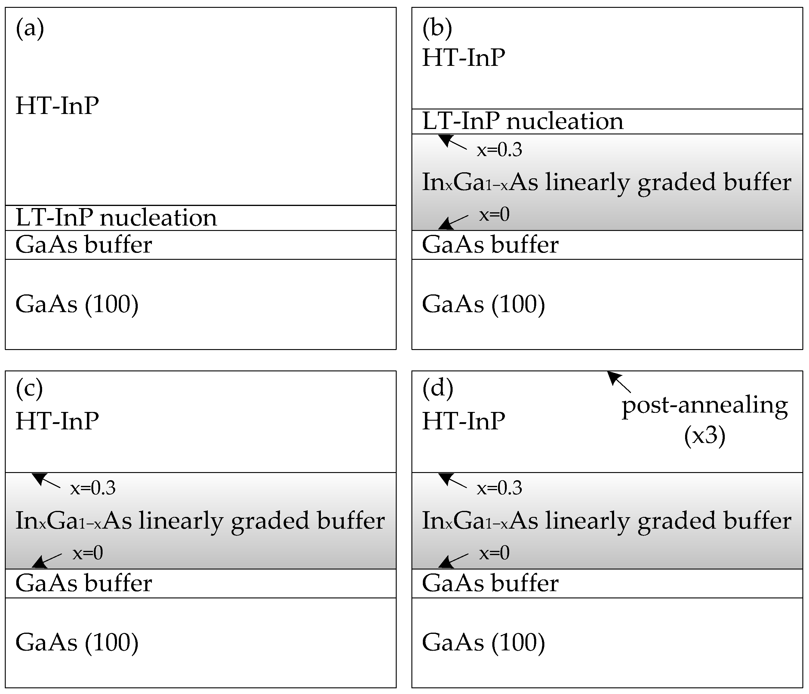
The growth of an InP/GaAs virtual substrate was carried out in a commercial low-pressure metalorganic chemical vapor deposition (MOCVD, AIX2800G4) [15]. Four inch Si-doped n-type (100) GaAs wafers with an orientation of 2° off toward <011> were used as substrates. Group-III precursors were trimethylgallium and trimethylindium. Pure phosphine (PH3) and arsine (AsH3) were the P and As sources. The carrier gas was purified hydrogen. As mentioned above, the two-step growth was simple and useful, but using only the method results in an InP/GaAs virtual substrate with a crystalline quality not qualified for device application. Therefore, a thin InGaAs linearly graded buffer layer combined with the two-step method was employed in this study to grow a good quality InP/GaAs virtual substrate. Figure 1 shows the schematic structures of InP/GaAs virtual substrates. Figure 1a is a traditional two-step InP/GaAs virtual substrate, and the structure was grown in a manner similar to the two-step method reported in other literature. A GaAs substrate was thermally cleaned in AsH3/H2 ambient at 600 °C for 5 min. After growing a 0.5-μm-thick GaAs regrowth layer, the substrate was then cooled down to 450 °C for the deposition of a 20-nm-thick LT-InP nucleation layer. The V/III ratio and growth rate of LT-InP were 77.4 and 0.6 μm/hr. The substrate was heated again to 650 °C for the growth of a 2-μm-thick HT-InP epilayer. The V/III ratio and growth rate of HT-InP were 61.1 and 1.2 μm/hr. Figure 1b shows an InP/GaAs virtual substrate grown using both two-step and InGaAs linearly graded buffer methods. Ideally, one can design an InGaAs graded buffer with an indium content changed linearly from zero to 53% (lattice matched to InP). However, an InGaAs graded buffer is proven to show phase separation, as the indium content is larger than 30% or more [14]. To avoid the phase separation, the InGaAs graded buffer layer in this study was changed linearly from zero to 30%, and the total thickness of the buffer was only 1.8 μm. The V/III ratios of LT- and HT-InP were the same as those in Figure 1a, and the thicknesses of LT- and HT-InP in Figure 1b were 20 nm and 1.6 μm. The structure in Figure 1c is the same as that in Figure 1b, except for the LT-InP nucleation layer. Figure 1d is the structure with additional three cycles of post-annealing. In a cycle of the post-annealing, the substrate was heated up to 735 °C in PH3/H2 ambient for 10 min and was then cooled down to 400 °C for two min. The flow rate of PH3 during annealing was 2.9 × 10⁻² mol/min.
2.2. Materials Characterization
A Bruker Innova atomic force microscope (AFM, Bruker, Santa Barbara, CA, USA) in tapping mode was employed to examine surface morphology and root-mean-square (RMS) roughness. A Bruker D8 Discover X-ray diffractometer (XRD, Bruker, Karlsruhe, Germany) was used to investigate the crystallinity of an InP/GaAs virtual substrate. The XRD analysis was performed with an X-ray source of Cu Kα radiation (λ = 1.5406 Å). The XRD beam size on the sample was about 2 mm × 20 mm, and the optical setup of the XRD instrument in this study was the same for all the samples. The transmission electron microscopy (TEM, JEOL, Tokyo, Japan) technique can be used to evaluate the dislocation density of an InP/GaAs virtual substrate. The TEM is a microscopy technique where a beam of electrons is transmitted through an ultrathin foil of a material, and interacts with the material. Unlike a perfect lattice, dislocations have different local atomic structures and produce a strain field, and therefore will cause the electron beam to scatter in different ways. As a consequence, contrast is generated in a TEM image. In this study, a JEOL JEM-2800F TEM instrument was utilized to examine both plan-view and cross-sectional images for evaluating threading dislocation density (TDD) in an InP/GaAs virtual substrate. The operation voltage of the TEM instrument was 200 kV, and the image was taken in scanning TEM bright-field mode. The TDD value is evaluated by counting the number of dislocation lines that thread a unit area in a TEM image. The TEM specimen preparation was carried out using an in-situ lift-out focused ion beam (FIB) technology. The operation voltage of the FIB instrument (Helios NanoLab 660, Hillsboro, OR, USA) was 30 kV, and gallium ions were used. In order to minimize the surface damage during FIB milling, the milling process was carried out using an initial accelerating voltage of 30 kV and a final voltage of 5 kV. The polishing was performed perpendicular to the foil thickness. The thinned sample was finally transferred to a molybdenum grid. The RT PL spectrum was measured using a Nanometrics RPM 2000 PL system with a 532 nm excitation laser to evaluate the optical property of an InP/GaAs virtual substrate.
3. Results and Discussion
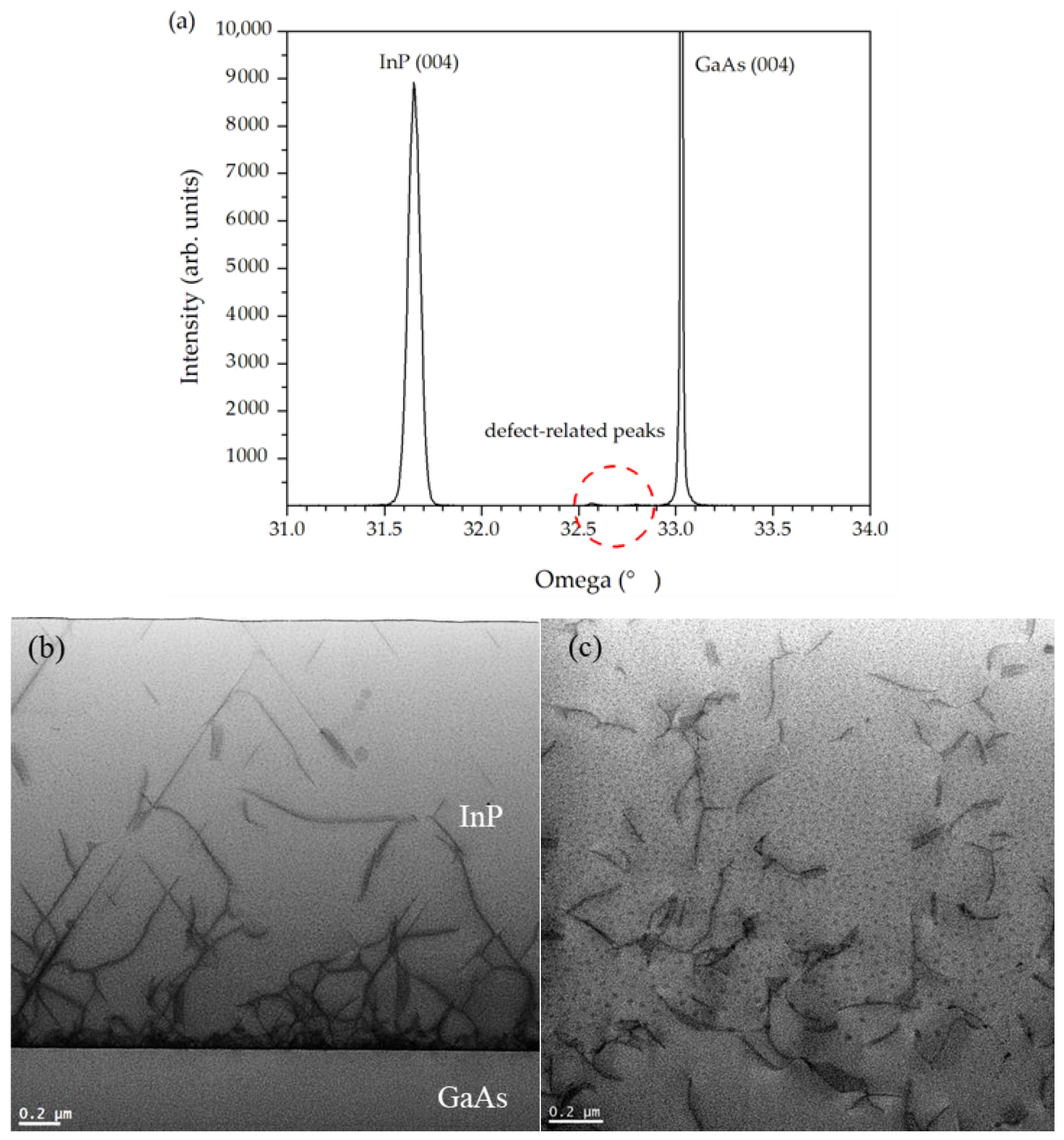
Before discussing the properties of an InP/GaAs virtual substrate grown using both an InGaAs linearly graded buffer structure and the two-step method, it is necessary to investigate the micro-structure of a traditional two-step InP/GaAs virtual substrate. Figure 2a shows an ω-2θ XRD scan of the structure in Figure 1a. One can see a dominant single-crystalline InP peak at the angle of ~31.65° and some very weak defect-related peaks which may originate from the LT-InP nucleation layer. The traditional two-step InP/GaAs virtual substrate was mirror-like, and the 3 × 3 μm2 RMS value was about 3.5 nm. These weak diffraction peaks in Figure 2a can be eliminated (data not shown here) via the method of recrystallization annealing on the LT-InP nucleation layer. Specifically, before the growth of the 2-μm-thick HT-InP epilayer, raising the substrate temperature from the LT-InP deposition temperature of 450 °C to 700 °C or higher for recrystallization annealing can obtain a pure single-crystalline InP peak at the angle of ~31.65° without any defect-related peaks. Figure 2b,c show cross-sectional and plan-view TEM images of the structure in Figure 1a. The cross-sectional TEM result reveals that the TDD near the InP top surface was about 1.0 × 109 cm−2, which is very close to the result of 1.5 × 109 cm−2 evaluating from the plan-view observation. These results reflect that using only the two-step method results in a smooth but high-TDD InP/GaAs virtual substrate. The origin of the high TDD value mainly relates to the large lattice mismatch of ~4% between InP and the underlying GaAs.
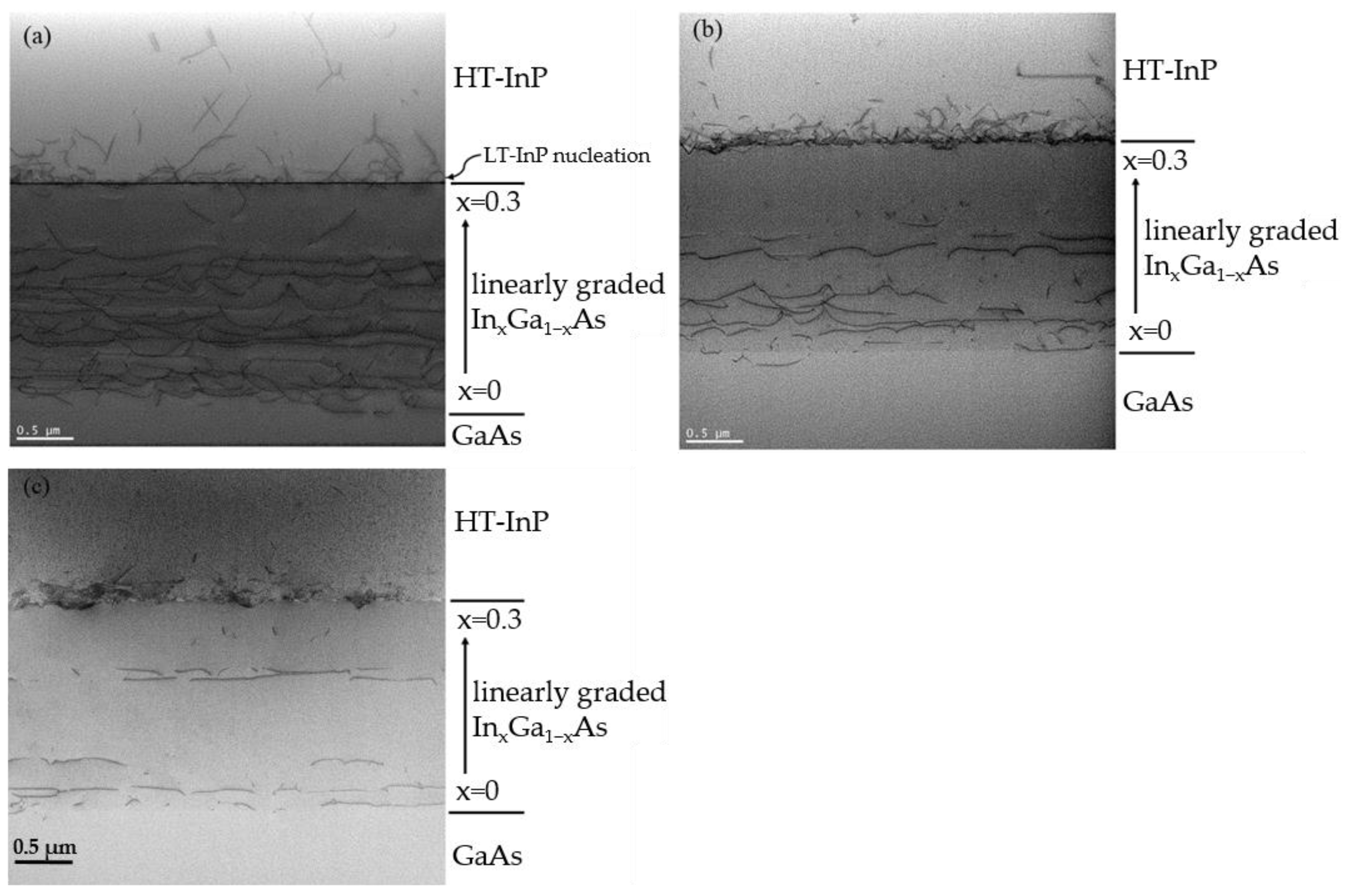
To reduce the dislocation density, one might intuitively think of growing InP on an InGaAs buffer with an indium composition as close as possible to 53%. However, an InGaAs buffer with an indium composition larger than 30% results in a phase separation phenomenon [14]. To avoid the phase separation, a 1.8-μm-thick InGaAs buffer with an indium composition linearly graded from zero to 30% was grown on GaAs, followed by the growth of two-step InP (Figure 1b). Figure 3a reveals a cross-sectional TEM microstructure of the InP/GaAs virtual substrate in Figure 1b. As expected, lattice strain relaxed through the formation of large numbers of misfit dislocations at the InGaAs/GaAs interface. The existing misfit dislocations elongated by gliding over many interfaces to relax the film. As the growth proceeded, an extremely low dislocation density was observed near the surface of the linearly graded InGaAs buffer. The observed stepwise distribution of dislocations in the linearly graded InGaAs buffer has been explained using a simple balance force model [16,17]. In addition, the interface between the LT-InP nucleation layer and the InGaAs buffer in Figure 3a was sharp. The TDD near the top surface of HT-InP was about 2.3 × 108 cm−2, which is much better than that in Figure 2b, indicating that reducing the lattice mismatch from InP/GaAs to InP/InGaAs significantly improves the crystallinity of HT-InP.
However, the TDD value of 2.3 × 108 cm−2 seems to still be high, and the reason for the high TDD is believed to relate to lattice mismatch and the defect-containing LT-InP nucleation layer. Therefore, another HT-InP sample was grown directly on the InGaAs linearly graded buffer without the deposition of an LT-InP nucleation layer (Figure 1c). The microstructure of the HT-InP sample is shown in Figure 3b. Again, one can see the nearly defect-free region near the top surface of the InGaAs buffer and the elongation of the misfit dislocations in the InGaAs bottom region by gliding over interfaces. However, the interface between HT-InP and the InGaAs buffer was relatively rough. Many misfit dislocations were also formed at the HT-InP/InGaAs interface. Only a few threading dislocations propagated into the top surface, and the TDD near the HT-InP top surface was 6.9 × 107 cm−2. To further reduce the TDD, a three-cycle post-annealing process was performed. Figure 3c shows the cross-sectional TEM image of the InP/GaAs virtual substrate in Figure 1. One can see a significant reduction of the dislocation density in the entire films and that the TDD near the HT-InP top surface was only 1.5 × 107 cm−2. The mechanism of the dislocation density reduction may relate to the annihilation or fusion of dislocations. In an annealing cycle, an InP/GaAs virtual substrate was heated up to 735 °C and was then cooled down to 400 °C. Because of the large difference in thermal expansion coefficient between InP and (In)GaAs, an InP film suffering intentionally large temperature variation changes its strain state periodically between compressive- and tensile-stress states. The thermal stresses may promote the motion of dislocations in the entire film. For adjacent dislocations with opposite Burgers vectors, they are likely to annihilate when encountering. Accordingly, the HT-InP sample in Figure 1d shows much better crystallinity than others. Our successful reduction in TDD from the initial 1.0 × 109 cm−2 for a pure two-step InP/GaAs virtual substrate to the value of only 1.5 × 107 cm−2 indicates that our proposed hybrid method is useful and comparable to other published work. Kimura et al. [8] showed a TDD value of 3.0 × 107 cm−2 for a 2-μm-thick InP/GaAs virtual substrate with a strained-layer superlattice. Morales et al. [10] reported a TDD value of ~108 cm−2 for a 2-μm-thick InP/GaAs virtual substrate after thermal annealing. Takano et al. [18] showed that the TDD near the InP surface was of the order of 107 cm−2 for a 3-μm-thick InP/GaAs virtual substrate.
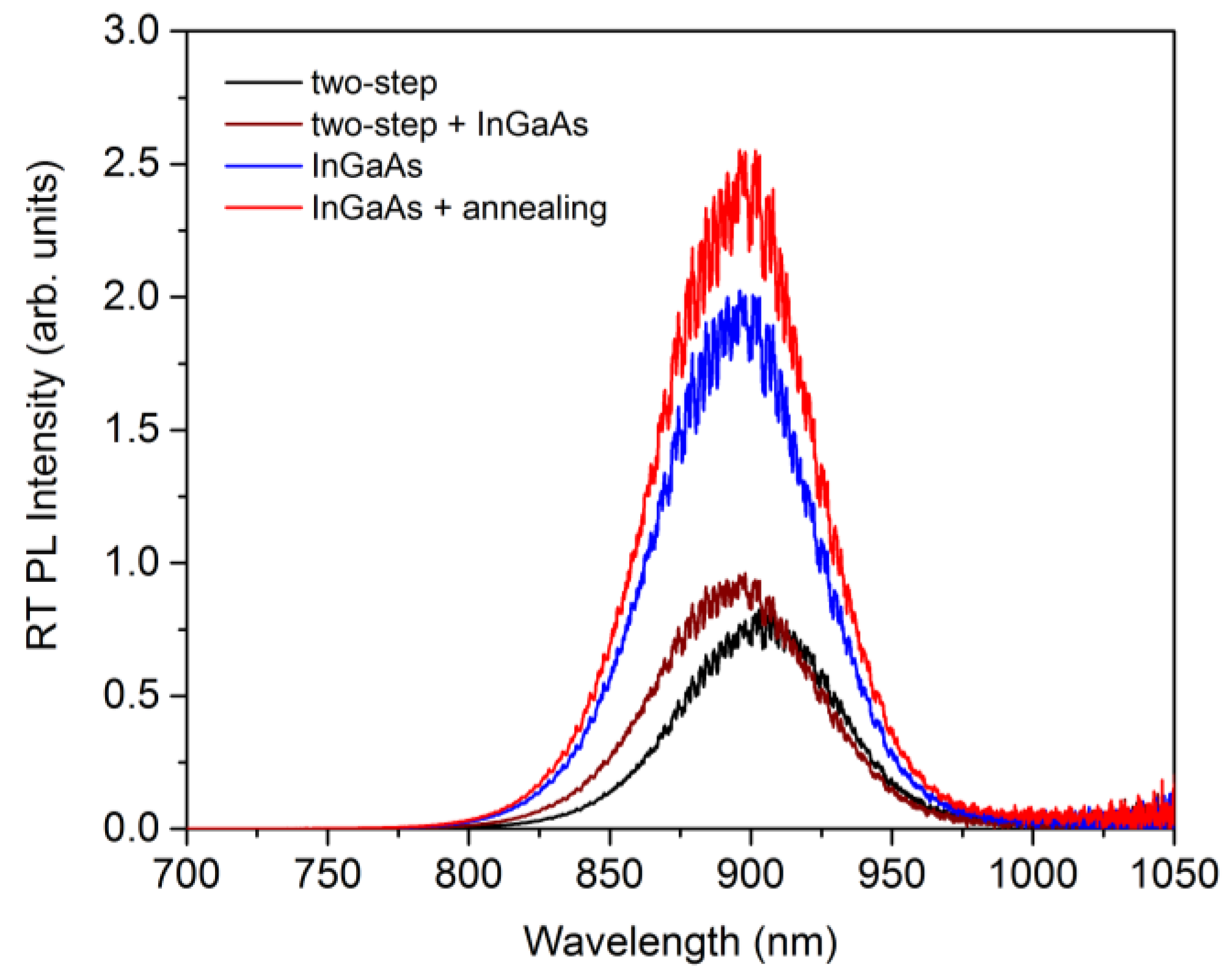
We further compared the optical properties of the InP/GaAs virtual substrates in Figure 1. The RT PL spectra of the HT-InP samples were measured with the same optical path. As shown in Figure 4, the HT-InP sample grown using only the two-step method showed the worst PL intensity. In contrast, the HT-InP sample grown using the InGaAs buffer and the post-annealing methods exhibited the strongest PL emission. The intensity variation of the RT PL spectra is in good agreement with the result observed from the TEM analysis. The tendency that the PL intensity increases inversely with the dislocation density was also reported in InP/GaAs [8] and InP/Si material systems [4]. The PL intensity improvement in this study may mainly come from dislocation density reduction because dislocations act as non-radiative recombination centers. The authors believe that the TDD value of 1.5 × 107 cm−2 for the InP/GaAs virtual substrate grown by combing the InGaAs linearly graded buffer and the post-annealing methods is good enough for the device application because Kimura et al. [8] reported a successful CW operation of an InGaAsP/InP double heterostructure laser diode grown on an InP/GaAs virtual substrate with a dislocation density of 3.0 × 107 cm−2. Although each method used in this study is not new, the authors skillfully combined these common methods to easily obtain high-quality InP/GaAs virtual substrates. We are now conducting experiments on the integration of optoelectronic devices on the InP/GaAs virtual substrates. We hope that the integration is beneficial to reducing device manufacturing costs in the future.
4. Conclusions
This paper has presented the epitaxial growth and characterization results of an InP/GaAs virtual substrate prepared using MOCVD. To overcome the lattice mismatch between InP and GaAs, the authors used a hybrid method including InGaAs graded buffer, two-step growth, and post-annealing. The traditional two-step InP/GaAs virtual substrate was smooth but had a high surface TDD of 1.5 × 109 cm−2. In contrast, the two-step InP grown on the InGaAs graded buffer showed a reduced TDD of 2.3 × 108 cm−2. By further removing the LT-InP nucleation layer and carrying out a post-annealing process, an InP/GaAs virtual substrate was grown with an improved TDD of 1.5 × 107 cm−2. With the successful reduction in TDD, the presented InP/GaAs virtual substrate showed improved PL intensity. The results of this study indicate that our hybrid method is simple and useful. This research may provide a useful reference for researchers attempting to integrate InP-related devices on GaAs substrates with reduced manufacturing costs.
Author Contributions
Conceptualization, Y.-L.T. and C.-H.W.; methodology, Y.-L.T.; investigation, Y.-L.T.; writing—original draft preparation, Y.-L.T.; writing—review and editing, C.-H.W.; project administration, C.-H.W. All authors have read and agreed to the published version of the manuscript.
Funding
This research was funded by the Ministry of Science and Technology (Taiwan, ROC)—grant number MOST 109-3111-Y-042A-007.
Institutional Review Board Statement
Not applicable.
Informed Consent Statement
Not applicable.
Data Availability Statement
The data presented in this study are available on request from the corresponding author.
Conflicts of Interest
The authors declare no conflict of interest.
References
- Liu, Y.; Wang, H.; Radhakrishnan, K. Increase in electron mobility of InGaAs/InP composite channel high electron mobility transistor structure due to SiN passivation. Thin Solid Film. 2007, 515, 4387–4389. [Google Scholar] [CrossRef]
- Touraton, M.L.; Martin, M.; David, S.; Bernier, N.; Rochat, N.; Moeyaert, J.; Loup, V.; Boeuf, F.; Jany, C.; Dutartre, D.; et al. Selective epitaxial growth of AlGaAs/GaAs heterostructures on 300 mm Si(001) for red optical emission. Thin Solid Film. 2021, 721, 138541. [Google Scholar] [CrossRef]
- Li, Q.; Ng, K.W.; Lau, K.M.; Tang, C.W.; Hill, R.; Vert, A. Defect reduction in epitaxial InP on nanostructured Si (001) substrates with position-controlled seed arrays. J. Cryst. Growth 2014, 405, 81–86. [Google Scholar] [CrossRef]
- Shi, B.; Klamkin, L. Defect engineering for high quality InP epitaxially grown on on-axis (001) Si. J. Appl. Phys. 2020, 127, 033102. [Google Scholar] [CrossRef]
- Cho, Y.D.; Lee, I.G.; Kim, S.W.; Jun, D.H.; Choi, I.H.; Kwon, H.M.; Shin, C.S.; Park, K.H.; Park, W.K.; Kim, D.H.; et al. Two-step growth of epitaxial InP layers by metalorganic chemical vapor deposition. J. Nanosci. Nanotechnol. 2016, 16, 5168–5172. [Google Scholar] [CrossRef] [PubMed]
- Derbali, M.B.; Meddeb, J.; Mâaref, H.; Buttard, D.; Abraham, P.; Monteil, Y. A comparative study of heterostructures InP/GaAs (001) and InP/GaAs (111) grown by metalorganic chemical vapor deposition. J. Appl. Phys. 1998, 84, 503. [Google Scholar] [CrossRef]
- Wang, Q.; Lu, J.; Xiong, D.; Zhou, J.; Huang, H.; Miao, A.; Cai, S.; Huang, Y.; Ren, X. Metamorphic In0.53Ga0.47As p-i-n photodetector grown on GaAs substrates by low-pressure MOCVD. Chin. Opt. Lett. 2007, 5, 358–360. [Google Scholar]
- Kimura, T.; Kimura, T.; Ishimura, E.; Uesugi, F.; Tsugami, M.; Mizuguchi, K.; Murotani, T. Improvement of InP crystal quality grown on GaAs substrates and device applications. J. Cryst. Growth 1991, 107, 827–831. [Google Scholar] [CrossRef]
- Hayafuji, N.; Kimura, T.; Yoshida, N.; Kaneno, N.; Tsugami, M.; Mizuguchi, K.; Murotani, T.; Ibuki, S. Improvement of InP crystal quality on GaAs substrates by thermal cyclic annealing. Jpn. J. Appl. Phys. 1989, 28, L1721–L1724. [Google Scholar] [CrossRef]
- Morales, F.M.; García, R.; Molina, S.I.; Aouni, A.; Postigo, P.A.; Fonstad, C.G. Microstructural improvements of InP on GaAs (001) grown by molecular beam epitaxy by in situ hydrogenation and postgrowth annealing. Appl. Phys. Lett. 2009, 94, 041919. [Google Scholar] [CrossRef] [Green Version]
- Fan, Y.B.; Wang, J.; Li, J.; Yin, H.Y.; Hu, H.Y.; Yang, Z.Y.; Wei, X.; Huang, Y.Q.; Ren, X.M. Epitaxial lateral overgrowth of InP on nanopatterned GaAs substrates by metal–organic chemical vapor deposition. J. Electron. Mater. 2018, 47, 5518–5524. [Google Scholar] [CrossRef]
- Sun, Y.; Dong, J.; Yu, S.; Zhao, Y.; He, Y. High quality InP epilayers grown on GaAs substrates using metamorphic AlGaInAs buffers by metalorganic chemical vapor deposition. J. Mater. Sci. Mater. Electron. 2017, 28, 745–749. [Google Scholar] [CrossRef]
- He, Y.; Yan, W.; Sun, Y.; Dong, J. Improved quality of InP layer on GaAs substrates by using compositionally modulated step-graded AlGaInAs buffers. J. Mater. Sci. Mater. Electron. 2019, 30, 16251–16256. [Google Scholar] [CrossRef]
- Quitoriano, N.J.; Fitzgerald, E.A. Relaxed, high-quality InP on GaAs by using InGaAs and InGaP graded buffers to avoid phase separation. J. Appl. Phys. 2007, 102, 033511. [Google Scholar] [CrossRef]
- Tsai, Y.L.; Yang, H.H.; Fang, J.H.; Chang, C.L.; Chen, M.H.; Wu, C.H.; Hong, H.F. GaAs-based optoelectronics grown on GaAs/Si virtual substrates with multiple spaced thermal-cycle annealing. Thin Solid Film. 2021, 733, 138817. [Google Scholar] [CrossRef]
- Song, Y.; Wang, S.; Tångring, I.; Lai, Z.; Sadeghi, M. Effects of doping and grading slope on surface and structure of metamorphic InGaAs buffers on GaAs substrates. J. Appl. Phys. 2009, 106, 123531. [Google Scholar] [CrossRef]
- Sorokin, S.V.; Klimko, G.V.; Sedova, I.V.; Sitnikova, A.A.; Kirilenko, D.A.; Baidakova, M.V.; Yagovkina, M.A.; Komissarova, T.A.; Belyaev, K.G.; Ivanov, S.V. Peculiarities of strain relaxation in linearly graded InxGa1−xAs/GaAs (001) metamorphic buffer layers grown by molecular beam epitaxy. J. Cryst. Growth 2016, 455, 83–89. [Google Scholar] [CrossRef]
- Takano, Y.; Sasaki, T.; Nagaki, Y.; Kuwahara, K.; Fuke, S.; Imai, T. Two-step growth of InP on GaAs substrates by metalorganic vapor phase epitaxy. J. Cryst. Growth 1996, 169, 621–624. [Google Scholar] [CrossRef]
Figure 1.
Schematic structure of an InP/GaAs virtual substrate prepared using (a) a two-step method; (b) an InGaAs linearly graded buffer combined with the two-step method; (c) the direct growth of HT-InP on the InGaAs linearly graded buffer; (d) the method “c” with additional three cycles of post-annealing.

Figure 2.
The characterization results of an InP/GaAs virtual substrate grown using a two-step method, including (a) an ω-2θ XRD scan; (b) a cross-sectional TEM image; (c) a plan-view TEM image.
Figure 2.
The characterization results of an InP/GaAs virtual substrate grown using a two-step method, including (a) an ω-2θ XRD scan; (b) a cross-sectional TEM image; (c) a plan-view TEM image.

Figure 3.
Cross-sectional TEM images of the virtual substrate plotted in (a) Figure 1b; (b) Figure 1c; (c) Figure 1d.

Figure 4.
The comparison of RT PL spectra of InP/GaAs virtual substrates grown using different approaches. The approaches used include the two-step method, an InGaAs buffer combined with the two-step, the direct growth of HT-InP on the InGaAs buffer, and the direct growth on the buffer with additional post-annealing.

Publisher’s Note: MDPI stays neutral with regard to jurisdictional claims in published maps and institutional affiliations. |
© 2022 by the authors. Licensee MDPI, Basel, Switzerland. This article is an open access article distributed under the terms and conditions of the Creative Commons Attribution (CC BY) license (https://creativecommons.org/licenses/by/4.0/).
Share and Cite
MDPI and ACS Style
Tsai, Y.-L.; Wu, C.-H. Reduced Dislocation Density of an InP/GaAs Virtual Substrate Grown by Metalorganic Chemical Vapor Deposition. Coatings 2022, 12, 723. https://0-doi-org.brum.beds.ac.uk/10.3390/coatings12060723
AMA Style
Tsai Y-L, Wu C-H. Reduced Dislocation Density of an InP/GaAs Virtual Substrate Grown by Metalorganic Chemical Vapor Deposition. Coatings. 2022; 12(6):723. https://0-doi-org.brum.beds.ac.uk/10.3390/coatings12060723
Chicago/Turabian StyleTsai, Yu-Li, and Chih-Hung Wu. 2022. "Reduced Dislocation Density of an InP/GaAs Virtual Substrate Grown by Metalorganic Chemical Vapor Deposition" Coatings 12, no. 6: 723. https://0-doi-org.brum.beds.ac.uk/10.3390/coatings12060723
Note that from the first issue of 2016, this journal uses article numbers instead of page numbers. See further details here.