
Large Transfer of Nitrogen, Silicon and Titanium through Various Thin Mo–Ti/Si and Ti–Mo/Si Bilayer Films Processed in Expanding Microwave Plasma: Formation of Nitrides and Silicides
Abstract
:1. Introduction
2. Materials and Methods
2.1. Mo–Ti/Si and Ti–Mo/Si Bilayer Films
- MoTi1 consists of a Ti film, 250 nm thick, coated on Si wafer and capped with a Mo film, 100 nm thick.
- TiMo1 consists or a Mo film, 50 nm thick, coated on Si wafer and capped with a Ti film, 250 nm thick.
- TiMo2 consists or a Mo film, 100 nm thick, coated on Si wafer and capped with a Ti film, 100 nm thick.
- TiMo3 consists or a Mo film, 250 nm thick, coated on Si wafer and capped with a Ti film, 50 nm thick.
- The samples (approximately 1 cm2) are then cut from the wafers with a diamond tip.
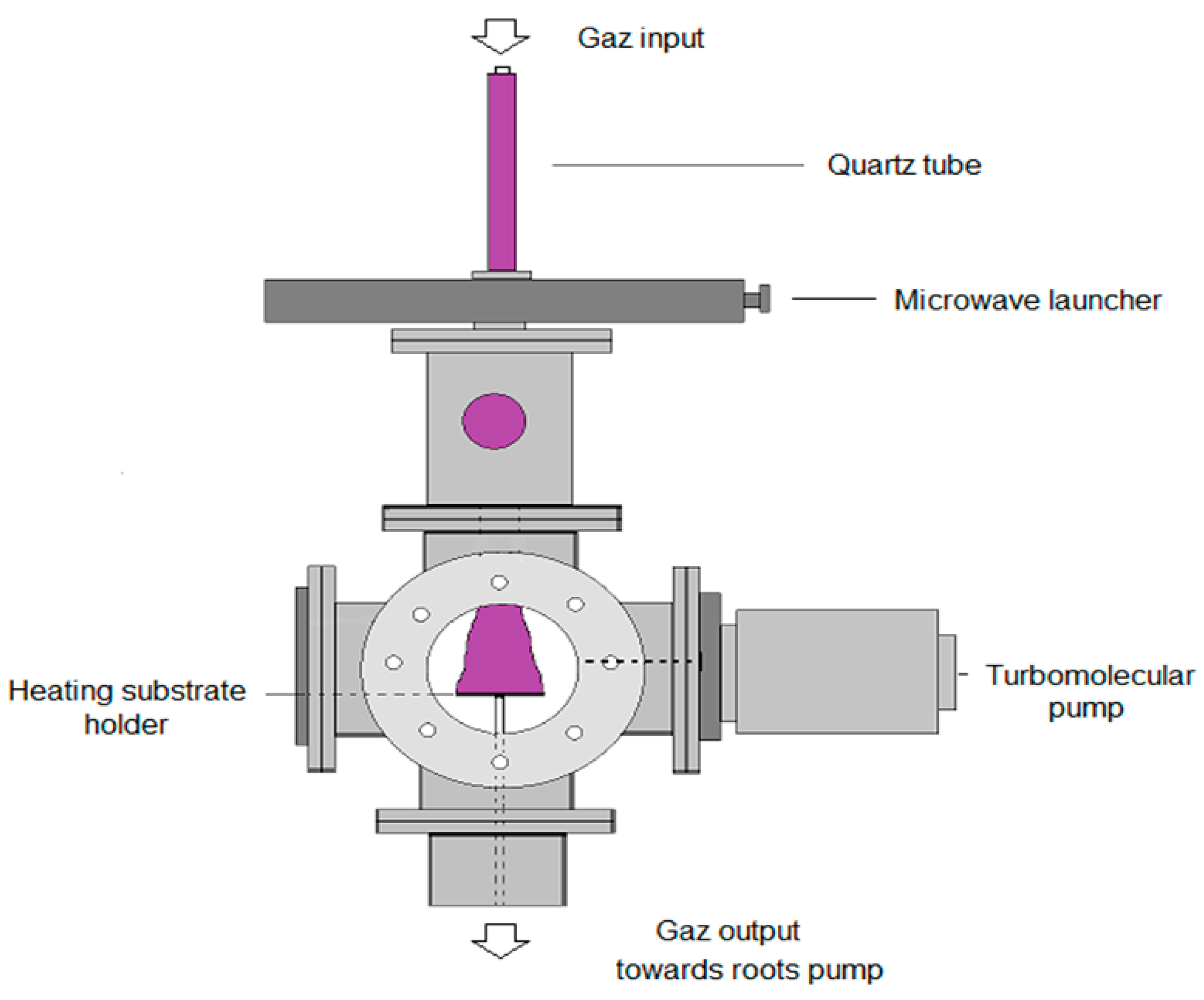
2.2. Thermochemical Treatment by Means of an Expanding Plasma Process
2.3. Investigations of Mo–Ti/Si and Ti–Mo/Si Bilayer Films
2.3.1. X-ray Diffraction Measurements
2.3.2. Raman Spectroscopy
2.3.3. Secondary Ion Mass Spectrometry Measurements
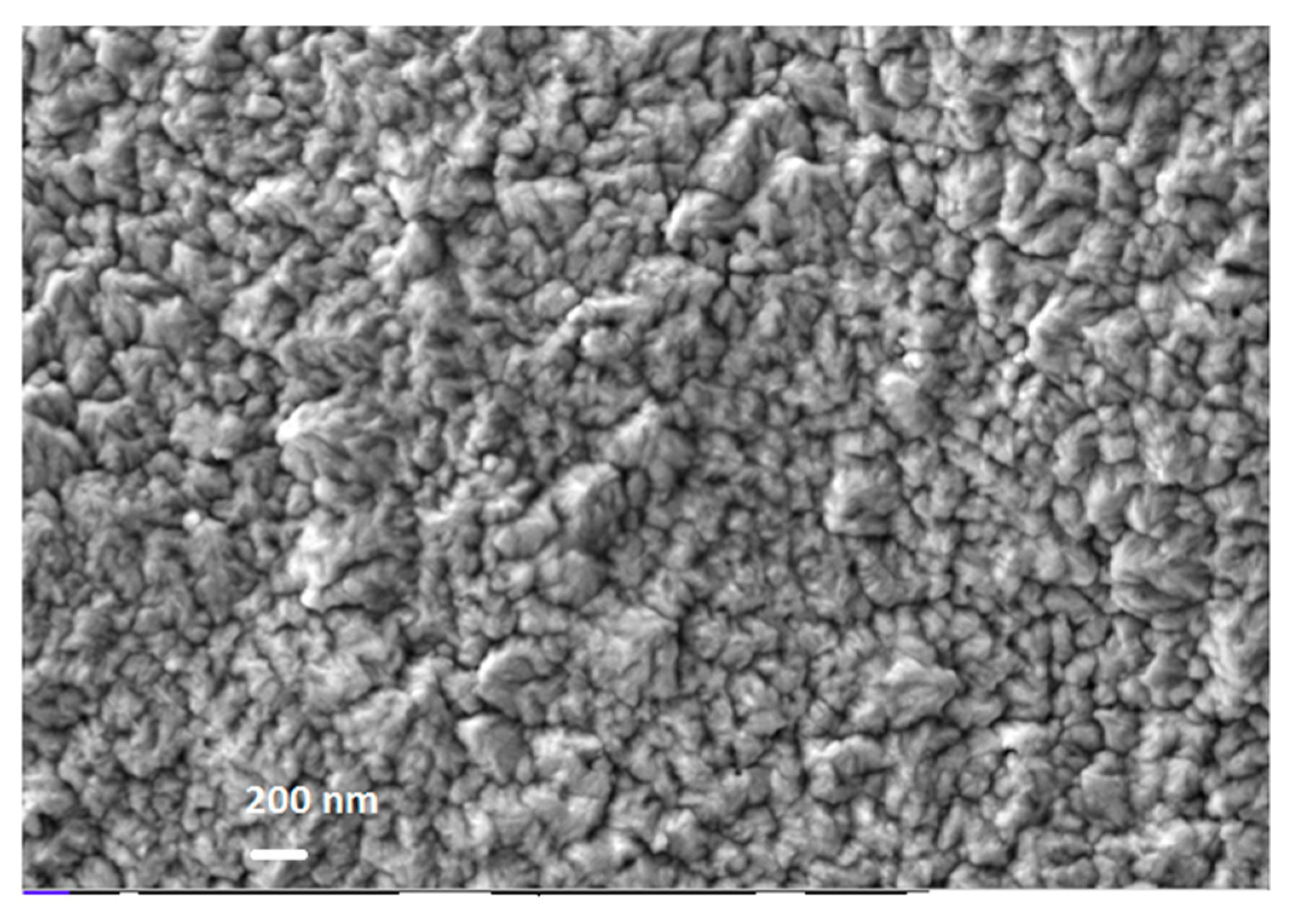
2.3.4. Scanning and Transmission Microscopy and Energy Dispersive Spectrometry
3. Results
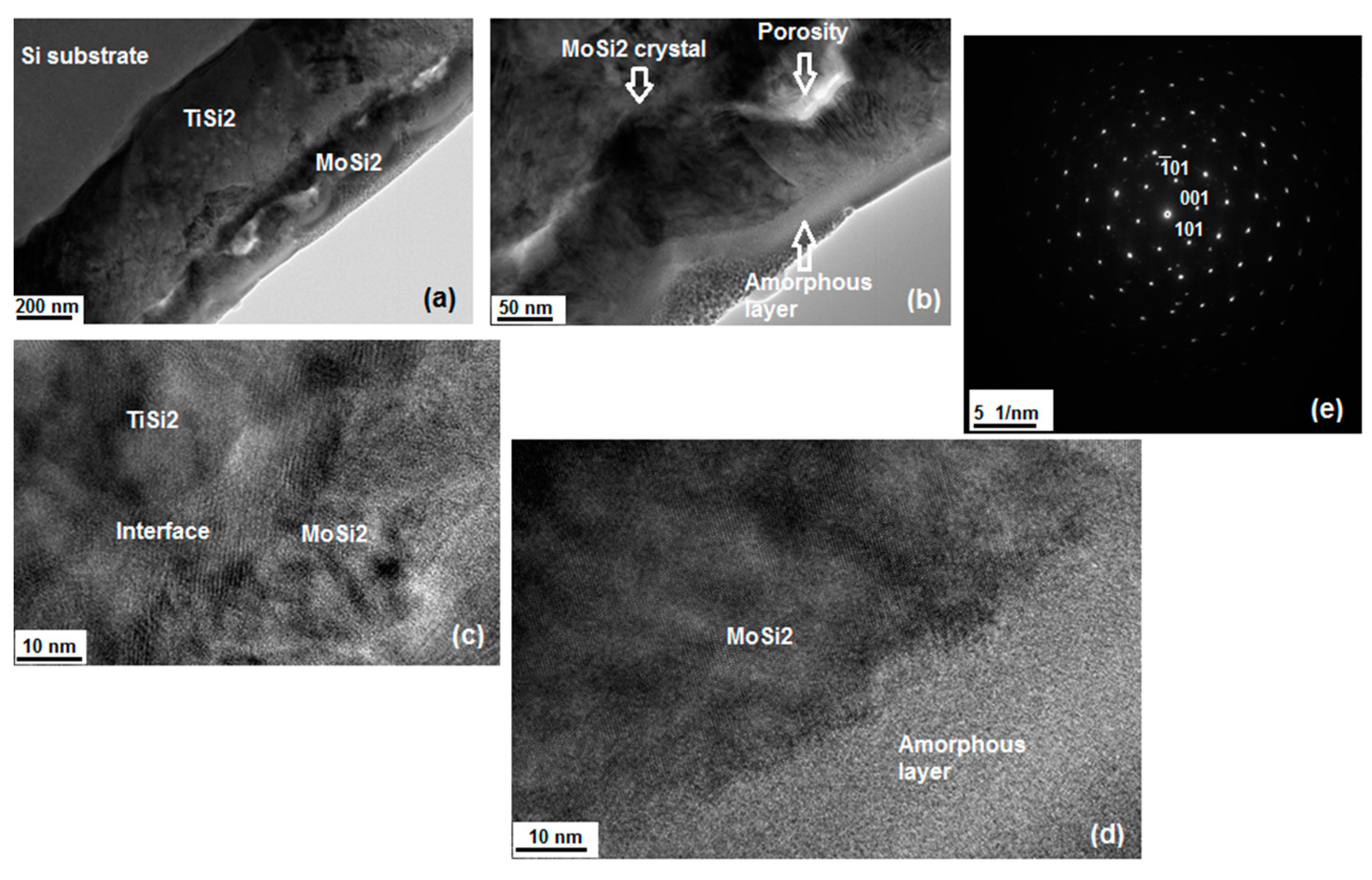
3.1. As-Received Mo–Ti/Si and Ti–Mo/Si Bilayer Thin Films
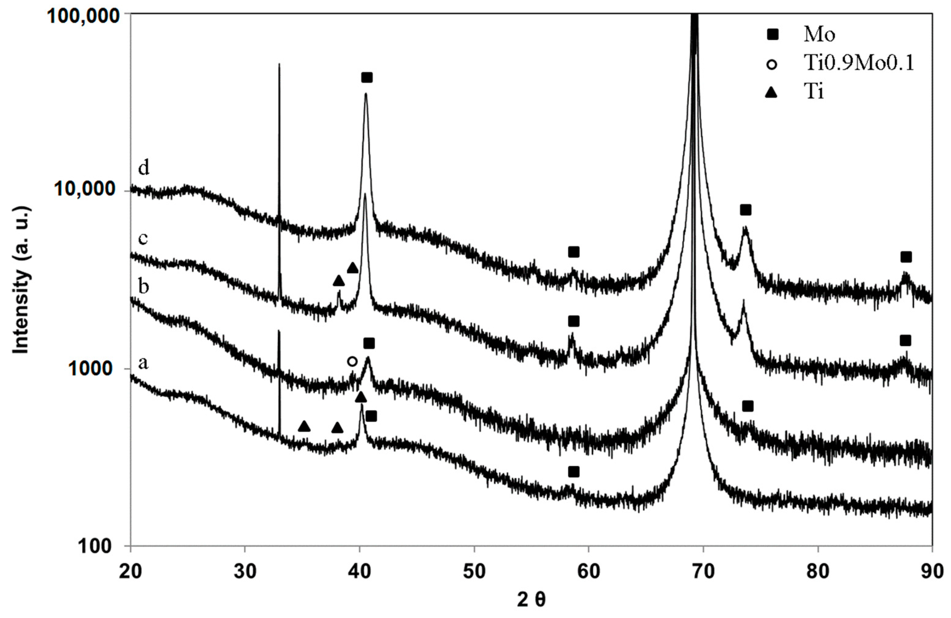
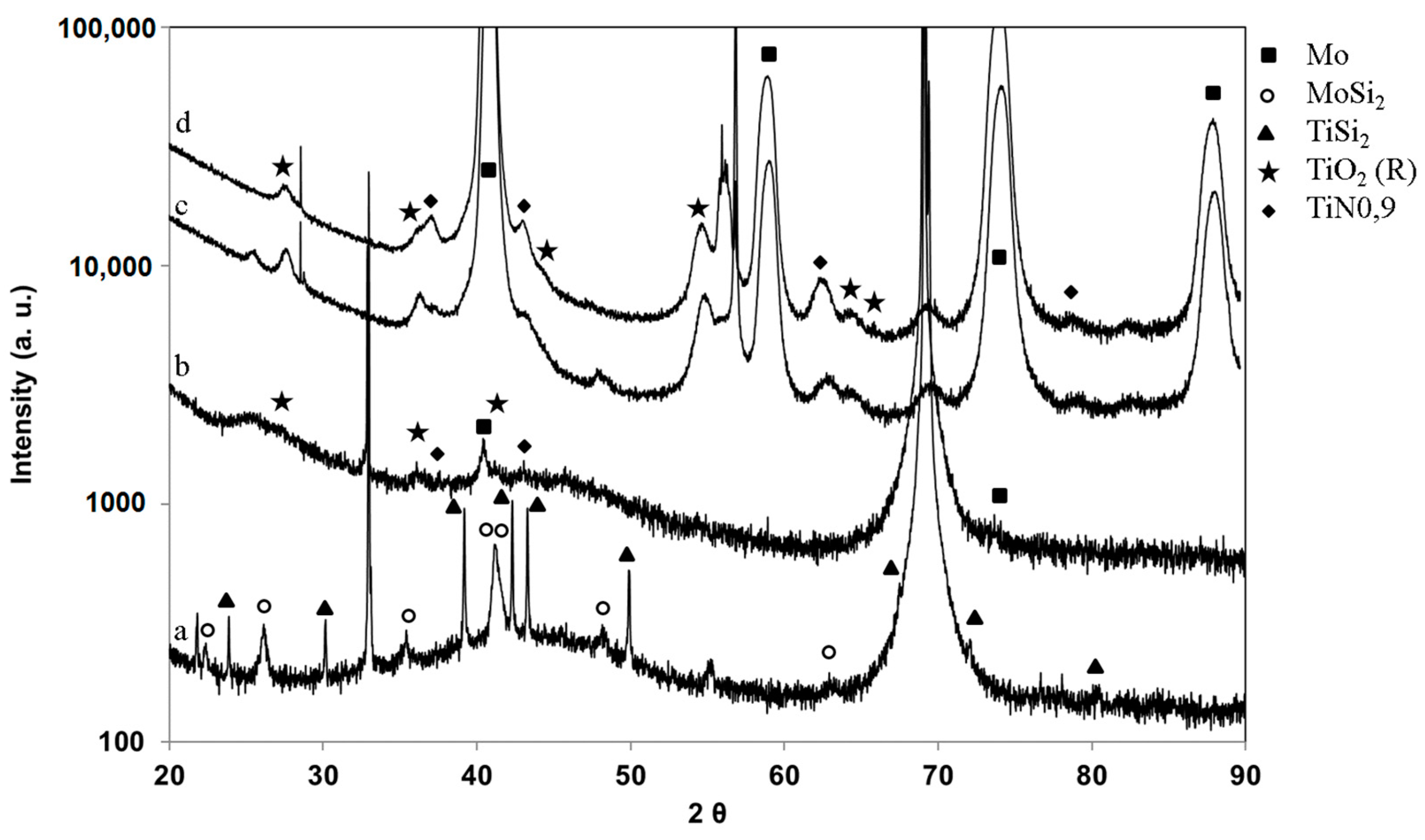
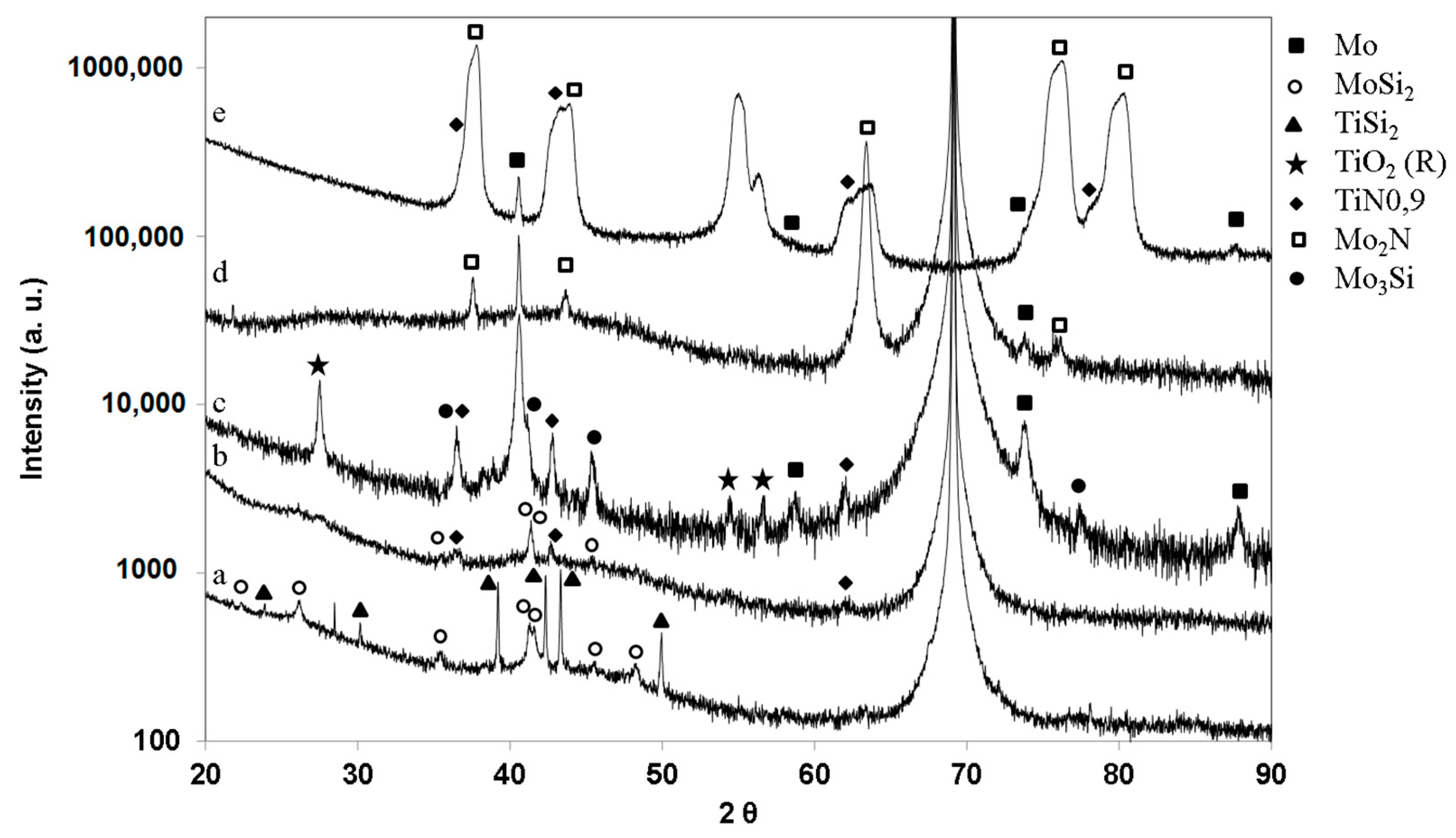
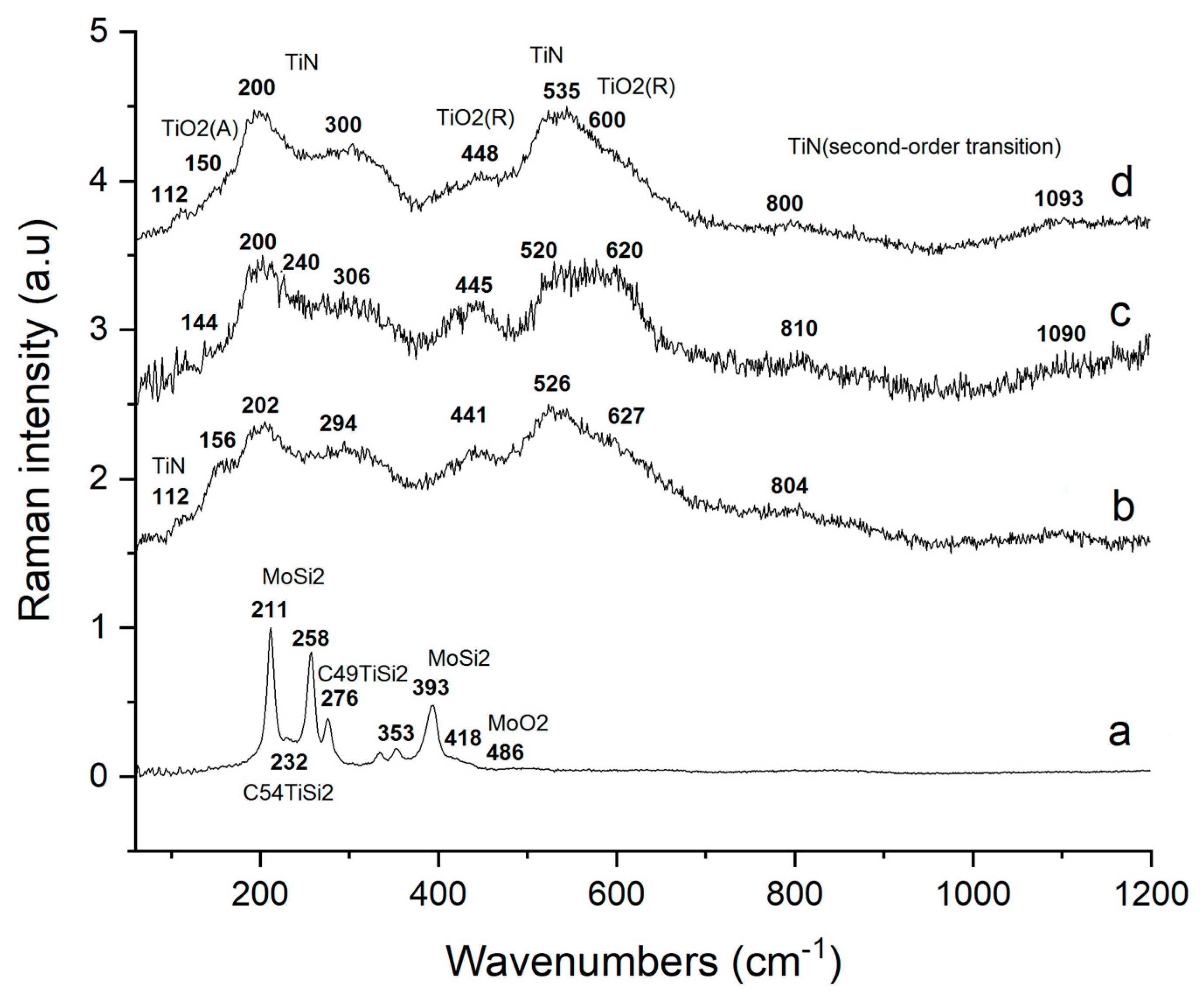
3.1.1. Crystalline Structure Analysis
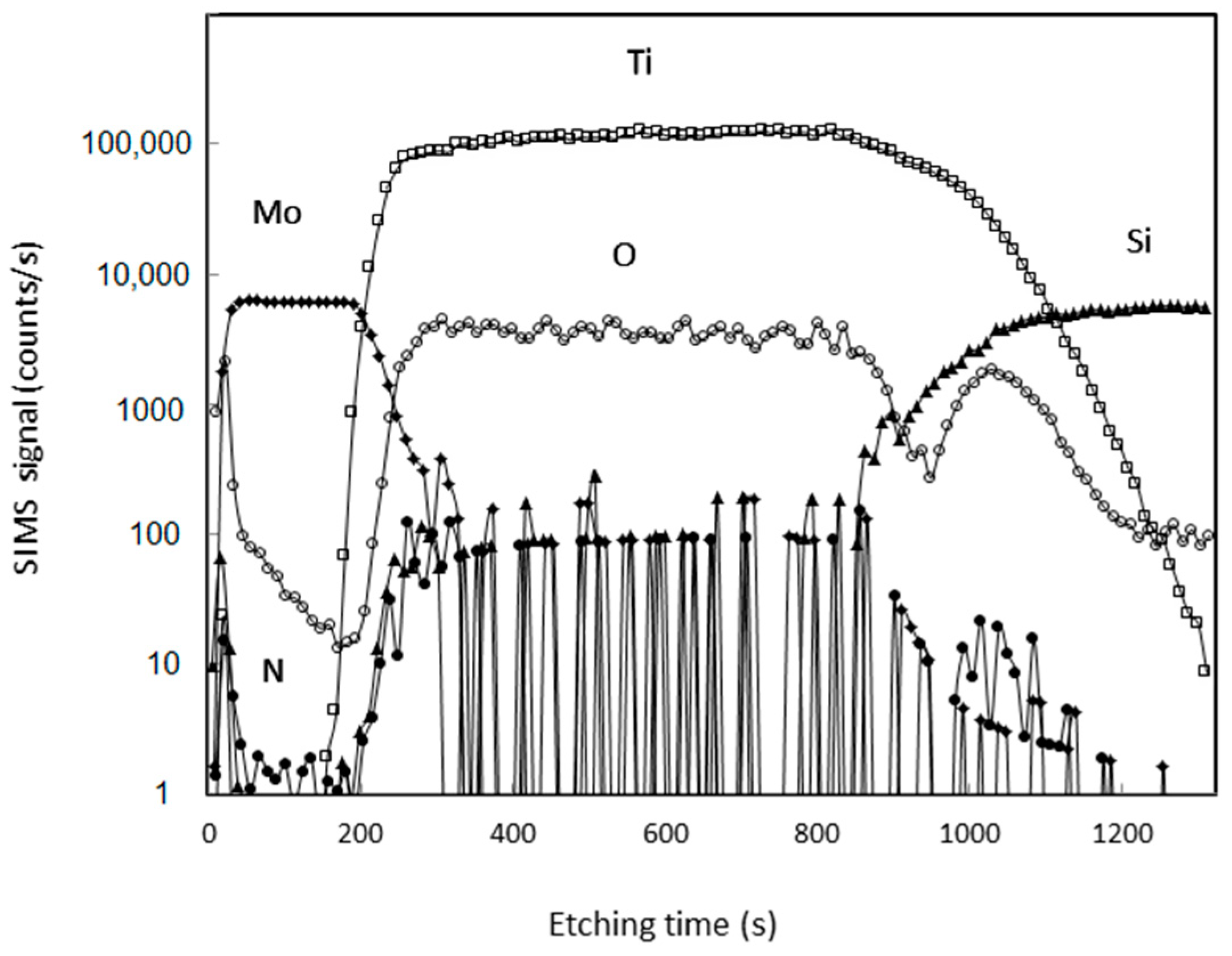
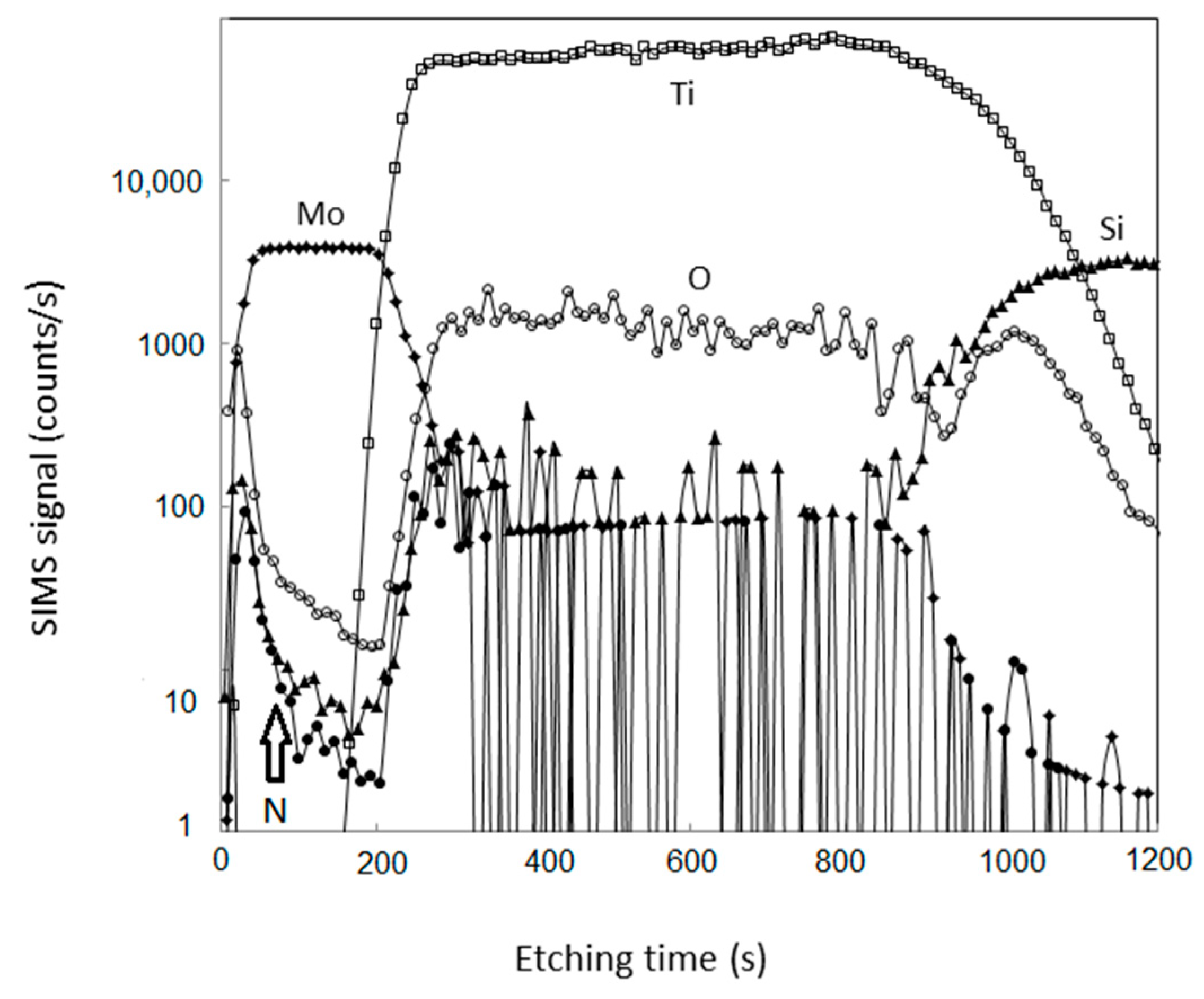
3.1.2. Diffusion of Elements
3.2. Mo–Ti and Ti–Mo Bilayer Films Exposed to (Ar-31%N2-6%H2) at 600 °C
3.2.1. Crystalline Structures
XRD Investigations
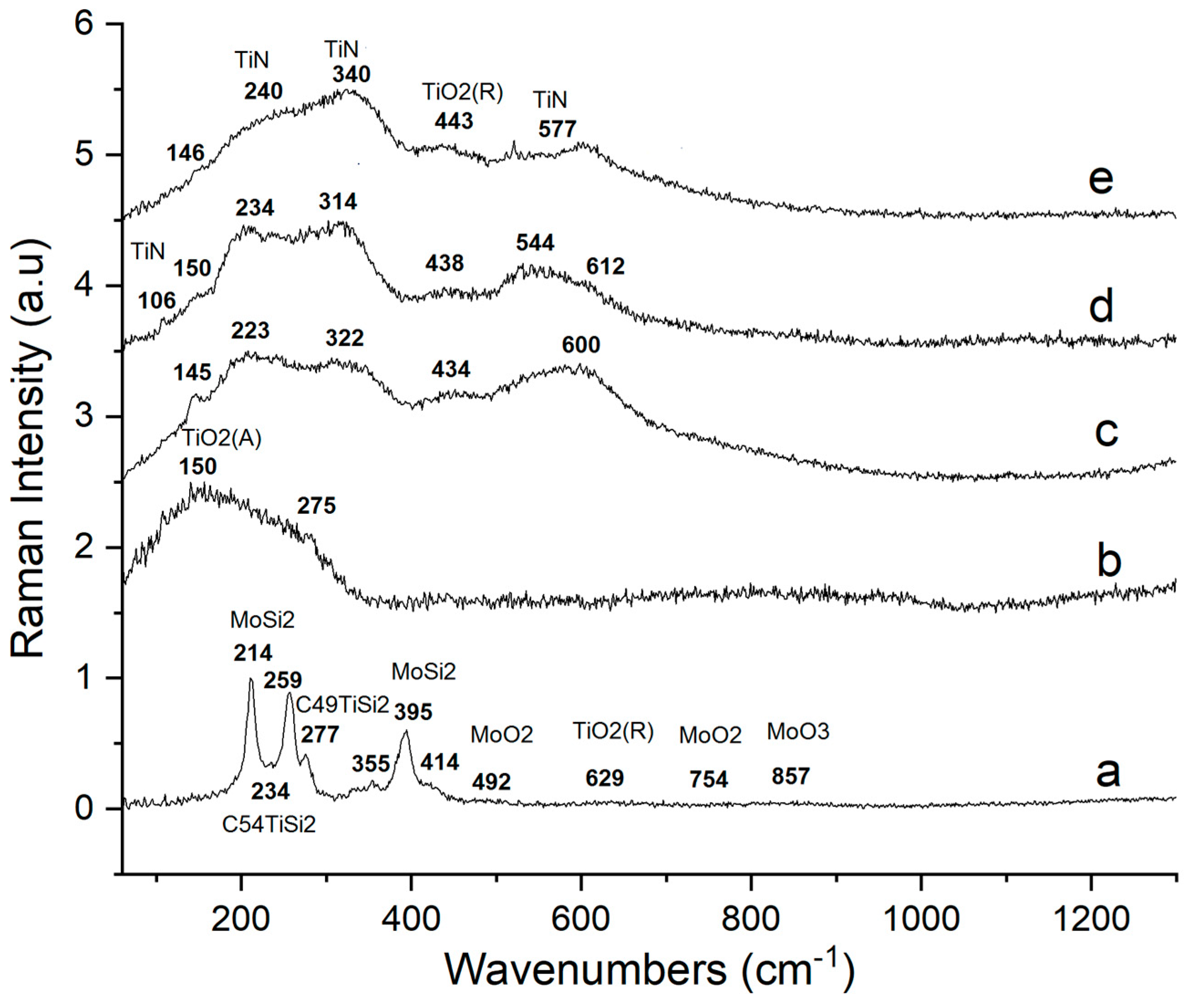
Raman Spectroscopy Investigations
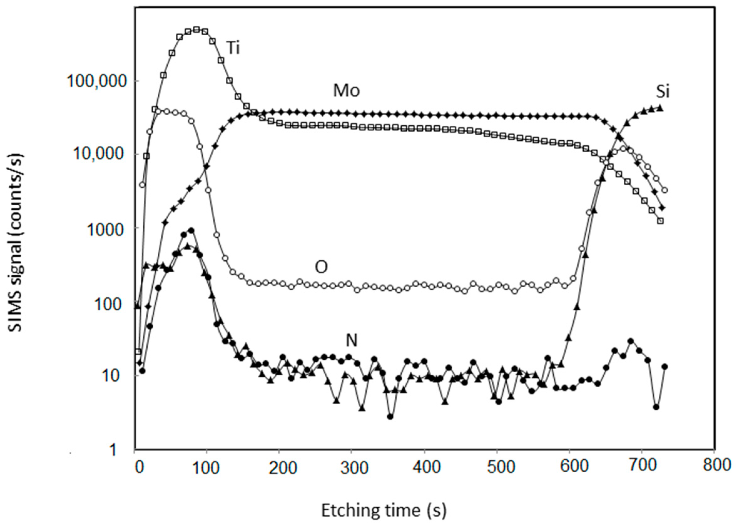
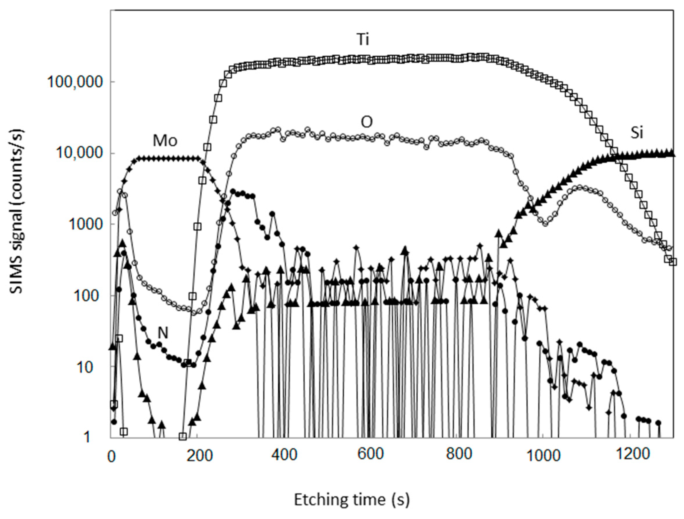
3.2.2. Diffusion of Elements
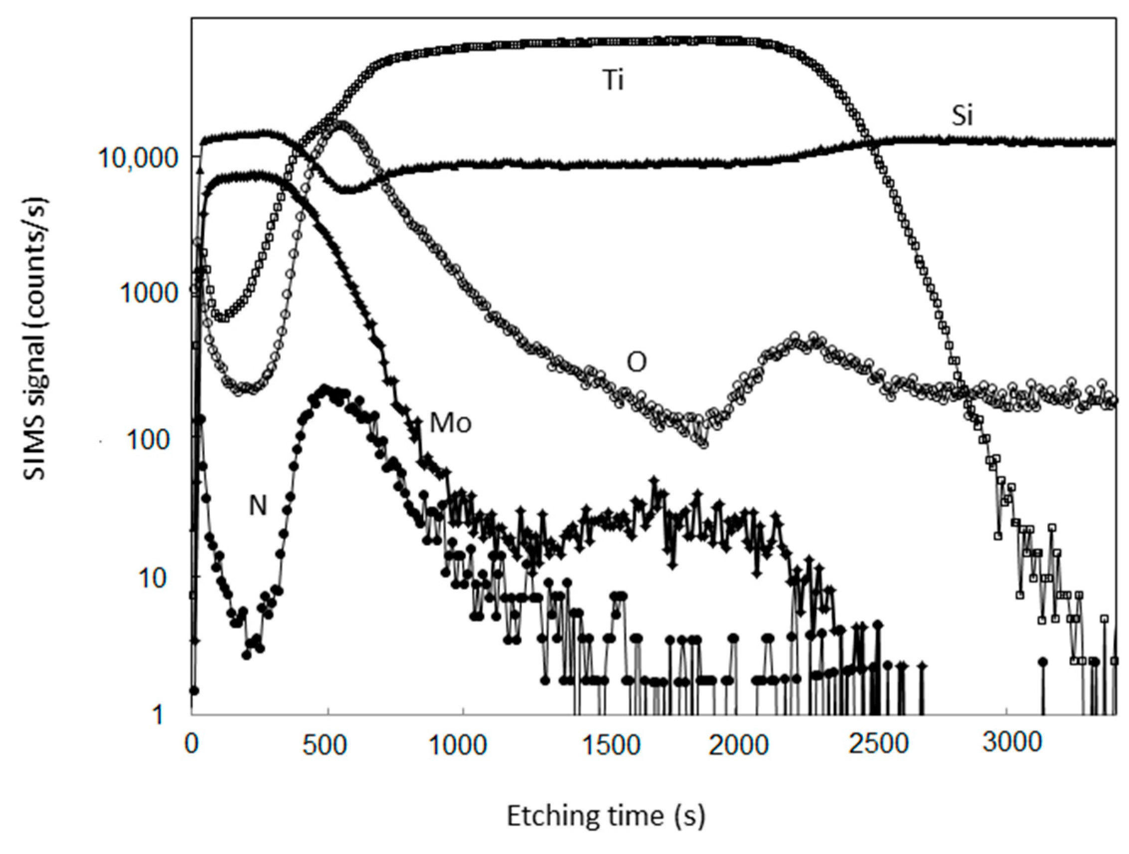
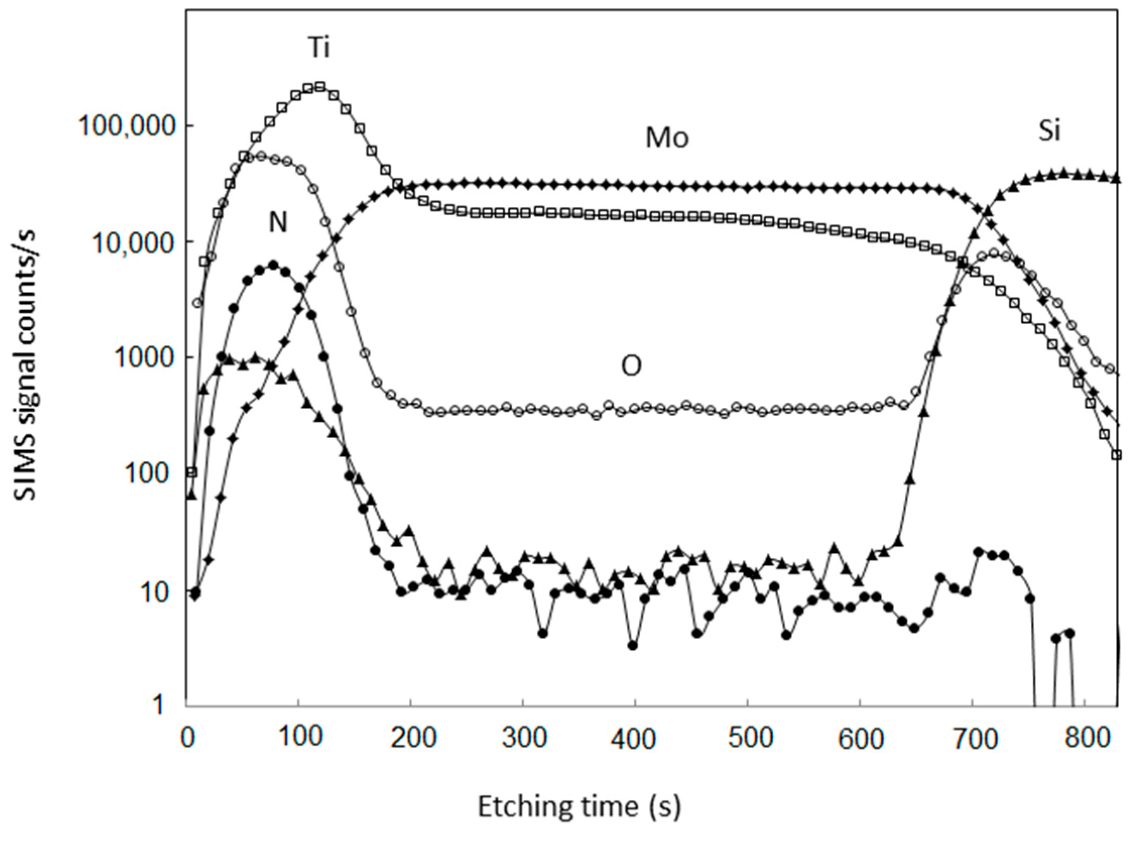
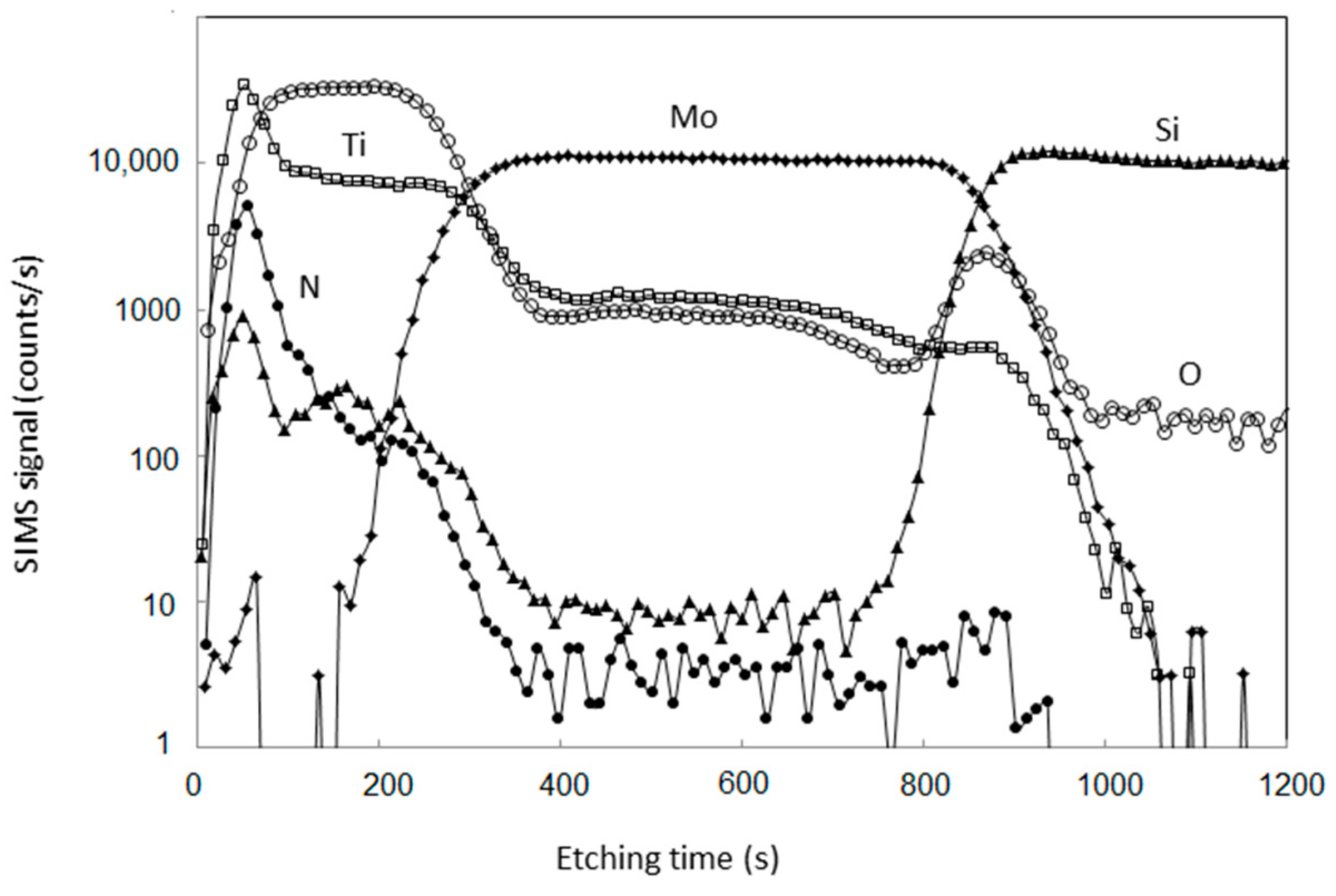
SIMS Measurements
EDS Measurements
3.2.3. Morphology and Microstructures of MoTi1 Bilayer Thin Films
3.3. Mo–Ti/Si and Ti–Mo/Si Bilayer Films Exposed to (Ar-31%N2-6%H2) at 800 °C
3.3.1. Crystalline Structures
XRD Investigations
Raman Spectroscopy Investigations
4. Discussion
5. Conclusions
Author Contributions
Funding
Acknowledgments
Conflicts of Interest
References
- Bhaskaran, M.; Sriram, S.; Short, K.T.; Mitchell, D.R.G.; Holland, A.S.; Reeves, G.K. Characterization of C54 titanium silicide thin films by spectroscopy, microscopy and diffraction. J. Phys. D Appl. Phys. 2007, 40, 5213–5219. [Google Scholar] [CrossRef]
- Jeon, H.; Sukow, C.A.; Honeycutt, J.W.; Rozgonyi, G.A.; Nemanich, R.J. Morphology and phase stability of TiSi2 on Si. J. Appl. Phys. 1992, 71, 4269–4276. [Google Scholar] [CrossRef]
- Yanisagawa, S.; Fukuyama, T. Preparation of molybdenum silicide films by reactive sputtering. J. Electrochem. Soc. 1980, 127, 1120–1124. [Google Scholar] [CrossRef]
- Ke-Ming, Y.; Jun-Xia, W.; Shi-Yuan, Y.; Xiu-Lu, Z.; Ping, L. In-situ synthesis of MoSi2 coating on Mo substrate under carbon protection and its short-term oxidation behavior. Surf. Coat. Technol. 2018, 354, 324–329. [Google Scholar] [CrossRef]
- Ohishi, Y.; Kurosaki, K.; Suzuki, T.; Muta, H.; Yamanaka, S.; Uchida, N.; Tada, T.; Kanayama, T. Synthesis of silicon and molybdenum-silicide nanocrystal composite films having low thermal conductivity. Thin Solid Films 2013, 534, 238–241. [Google Scholar] [CrossRef]
- Liu, Z.; Luo, B.; Hu, J.; Xing, C. Transport mechanism in amorphous molybdenum silicide thin films. J. Phys. Chem. Solids 2021, 149, 109818. [Google Scholar] [CrossRef]
- Iyer, S.S.; Ting, C.Y.; Fryer, P.M. Ambient gas effects on the reaction of titanium with silicon. J. Electrochem. Soc. 1985, 132, 2240–2245. [Google Scholar] [CrossRef]
- Tsai, J.Y.; Apte, P. A thickness model for the TiSi2/TiN stack in the titanium silicide process module. Thin Solid Films 1995, 270, 589–595. [Google Scholar] [CrossRef]
- Lee, W.G.; Lee, J.G. Enhancement of TiSi2 formation during rapid thermal annealing in N2 by the presence of native oxide. J. Electrochem. Soc. 2002, 149, G1–G7. [Google Scholar] [CrossRef]
- Wang, L.L.; Peng, W.; Jiang, Y.L.; Li, B.Z. Effective Shottky barrier height lowering by TiN capping layer for TiSix/Si power diode. IEEE Electron Device Lett. 2015, 36, 597–599. [Google Scholar] [CrossRef]
- Oyama, S.T. Introduction to the chemistry of transition metal carbides and nitrides. In The Chemistry of Transition Carbides and Nitrides, 1st ed.; Oyama, S.T., Ed.; Blackie Academic and Professional: London, UK, 1996; pp. 2–10. [Google Scholar]
- Jauberteau, I.; Bessaudou, A.; Mayet, R.; Cornette, J.; Jauberteau, J.L.; Carles, P.; Merle-Mejean, T. Molybdenum nitride films: Crystal structures, synthesis, mechanical, electrical and some other properties. Coatings 2015, 5, 656–687. [Google Scholar] [CrossRef]
- Ozsdolay, B.D.; Balasubramanian, K.; Gall, D. Cation and anion vacancies in cubic molybdenum nitride. J. All. Com. 2017, 705, 631–637. [Google Scholar] [CrossRef]
- Ponon, N.K.; Appleby, D.J.R.; Arac, E.; King, P.J.; Ganti, S.; Kwa, K.S.K.; O’Neill, A. Effect of deposition conditions and postdeposition anneal on reactively sputtered titanium nitride films. Thin Solid Films 2015, 578, 31–37. [Google Scholar] [CrossRef]
- Lima, L.P.B.; Diniz, J.A.; Doi, I.; Godoy Fo, J. Titanium nitride as electrode for MOS technology and Schottky diode: Alternative extraction method of titanium nitride work function. Microelectron. Eng. 2012, 92, 86–90. [Google Scholar] [CrossRef]
- Xiang, W.; Zhao, C.; Liu, K.; Zhang, G.; Zhao, K. Heteroepitaxial growth of TiN thin films on Si substrates for MEMS applications. J. Alloys Compd. 2016, 658, 862–866. [Google Scholar] [CrossRef]
- Tagliazucca, V.; Schlichte, K.; Schüth, F.; Weidenthaler, C. Molybdenum-based catalysts for the decomposition of ammonia: In situ X-ray diffraction studies, microstructure, and catalytic properties. J. Catal. 2013, 305, 277–289. [Google Scholar] [CrossRef]
- Tagliazucca, V.; Leoni, M.; Weidenthaler, C. Crystal structure and microstructural changes of molybdenum nitrides traces during catalytic reaction by in situ X-ray diffraction studies. Phys. Chem. Chem. Phys. 2014, 16, 6182–6188. [Google Scholar] [CrossRef]
- Zhu, J.F.; Guo, J.C.; Zhai, R.S.; Bao, X.; Zhang, X.Y.; Zhuang, S. Preparation and adsorption properties of Mo2N model catalyst. Appl. Surf. Sci. 2000, 161, 86–93. [Google Scholar] [CrossRef]
- Zhou, Y.; Guo, W.; Li, T. A review on transition metal nitrides as electrode materials for supercapacitors. Ceram. Int. 2019, 45, 21062–21076. [Google Scholar] [CrossRef]
- Xiong, Z.; Yang, J.; Gao, Z.; Yang, Q.; Shi, D. Orthorhombic Mo3N2 nanobelts with improved properties as electrode material for supercapacitors. Results Phys. 2020, 16, 102941. [Google Scholar] [CrossRef]
- Bernie Ting, Y.-J.; Wu, H.; Kherani, N.P.; Lian, K. Development of pseudocapacitive molybdenum oxide-nitride for electrochemical capacitors. Mater. Chem. Phys. 2015, 154, 118–124. [Google Scholar] [CrossRef]
- Gu, M.; Bai, S.; Xia, X.; Huang, X.; Li, X.; Shi, X.; Chen, L. Study of the high temperature interfacial stability of Ti/Mo/Yb0.3Co4Sb12 thermoelectric joints. Appl. Sci. 2017, 7, 952. [Google Scholar] [CrossRef]
- Bernie Ting, Y.-J.; Lian, K.; Kherani, N. Fabrication of titanium nitride and molybdenum nitride for supercapacitor electrode application. ECS Trans. 2011, 35, 133–139. [Google Scholar] [CrossRef]
- Xie, Y.; Tian, F. Capacitive performance of molybdenum nitride/titanium nitride nanotube array for supercapacitor. Mater. Sci. Eng. B 2017, 215, 64–70. [Google Scholar] [CrossRef]
- Klimashin, F.F.; Koutna, N.; Euchner, H.; Holec, D.; Mayrhofer, P.H. The impact of nitrogen content and vacancies on structure and mechanical properties of Mo-N thin films. J. Appl. Phys. 2016, 120, 185301. [Google Scholar] [CrossRef]
- Jauberteau, I.; Mayet, R.; Cornette, J.; Mangin, D.; Bessaudou, A.; Carles, P.; Jauberteau, J.L.; Passelergue, A. Silicides and nitrides formation in Ti films coated on Si and exposed to (Ar-N2-H2) expanding plasma. Coatings 2017, 7, 23. [Google Scholar] [CrossRef]
- Jauberteau, I.; Carles, P.; Mayet, R.; Cornette, J.; Bessaudou, A.; Jauberteau, J.L. Competing growth of titanium nitrides and silicides in Ti films processed in expanding microwave plasma: Morphology and microstructural properties. AIP Adv. 2018, 8, 095105. [Google Scholar] [CrossRef]
- Jauberteau, I.; Mayet, R.; Cornette, J.; Carles, P.; Mangin, D.; Bessaudou, A.; Jauberteau, J.L.; Passelergue, A. Expanding plasma process for nitriding Mo-Ti bilayer thin films. Coatings 2019, 9, 96. [Google Scholar] [CrossRef]
- Jauberteau, I.; Mayet, R.; Cornette, J.; Bessaudou, A.; Carles, P.; Jauberteau, J.L.; Merle-Méjean, T. A reduction-nitridation process of molybdenum films in expanding microwave plasma: Crystal structure of molybdenum nitrides. Surf. Coat. Technol. 2015, 270, 77–85. [Google Scholar] [CrossRef]
- Zaumseil, P. High resolution characterization of the forbidden Si(200) and Si(222) reflections. J. Appl. Cryst. 2015, 48, 528–532. [Google Scholar] [CrossRef]
- Wang, J.; Coppari, F.; Smith, R.F.; Eggert, J.H.; Lazicki, A.E.; Fratanduono, D.E.; Rygg, J.R.; Boelhy, T.R.; Collins, G.W.; Duffy, T.S. X-ray diffraction of molybdenum under shock compression to 450 GPa. Phys. Rev. B 2015, 62, 174114. [Google Scholar] [CrossRef]
- Oliveira, N.T.C.; Aleixo, G.; Caram, R.; Guastaldi, A.C. Development of Ti-Mo alloys for biomedical applications: Microstructures and electrochemical characterization. Mater. Sci. Eng. A 2007, 452–453, 727–731. [Google Scholar] [CrossRef]
- Simka, W.; Krzakala, A.; Korotin, D.M.; Zhidkov, I.S.; Kurmaev, E.Z.; Cholakh, S.O.; Kuna, K.; Dercz, G.; Michalska, J.; Suchanek, K.; et al. Modification of a Ti-Mo alloy surface via plasma electrolytic oxidation in a solution containing calcium and phosphorus. Electrochem. Acta 2013, 96, 180–190. [Google Scholar] [CrossRef]
- Zhang, W.-D.; Liu, Y.; Wu, H.; Song, M.; Zhang, X.-D.; Lan, X.-D.; Yao, T.-H. Elastic modulus of phases in Ti-Mo alloys. Mater. Charact. 2015, 106, 302–309. [Google Scholar] [CrossRef]
- Kislitin, S.B.; Potekaev, A.I.; Uglov, V.V.; Klopotov, A.A.; Klopotov, V.D.; Ivanov, Y.F.; Parpiev, A.T. Steel suface TiCrN, TiMoN coatings structural phase state change features after low-energy alpha particles irradiation. IOP Conf. Ser. Mater. Sci. Eng. 2018, 289, 012010. [Google Scholar] [CrossRef]
- Nemanich, R.J.; Fiordalice, R.W.; Jeon, H. Raman scattering characterization of titanium silicide formation. IEEE J. Quantum Electron. 1989, 25, 997–1002. [Google Scholar] [CrossRef]
- Barhai, P.K.; Kumari, N.; Banerjee, I.; Pabi, S.K.; Mahapatra, S.K. Study of the effect of plasma current density on the formation of titanium nitride ant titanium oxynitride thin films prepared by reactive DC magnetron sputtering. Vacuum 2010, 84, 896–901. [Google Scholar] [CrossRef]
- Birtill, J.J.; Dickens, P.G. Thermochemistry of hydrogen molybdenum bronze phases HxMoO3. J. Solid State Chem. 1979, 29, 367–372. [Google Scholar] [CrossRef]
- Zhang, S.-L.; Lavoie, C.; Cabral, C.; Harper, J.M.E.; d’Heurle, F.M.; Jordan-Sweet, J. In situ characterization of titanium silicide formation: The effect of Mo interlayer, temperature ramp-rate, and annealing atmosphere. J. Appl. Phys. 1999, 85, 2617–2626. [Google Scholar] [CrossRef]
- Chaix-Pluchery, O.; Chenevier, B.; Matko, I.; Senateur, J.P.; La Via, F. Investigations of transient phase formation in Ti/Si thin film reaction. J. Appl. Phys. 2004, 96, 361–368. [Google Scholar] [CrossRef]
- Doland, C.M.; Nemanich, R.J. Phase formation during reactive molybdenum-silicide formation. J. Mater. Res. 1990, 5, 2854–2864. [Google Scholar] [CrossRef]
- Wdowik, U.D.; Twardowska, A.; Medala-Wasik, M. Lattice dynamics of binary and ternary phases in Ti-Si-C system: A combined Raman spectroscopy and density functional theory study. Mater. Chem. Phys. 2015, 168, 58–65. [Google Scholar] [CrossRef]
- Dieterle, M.; Mestl, G. Raman spectroscopy of molybdenum oxides. Phys. Chem. Chem. Phys. 2002, 4, 812–826. [Google Scholar] [CrossRef]
- Teoh, L.G.; Lee, Y.C.; Chang, Y.S.; Fang, T.H.; Chen, H.Q. Preparation and characterization of nanocrystalline titanium dioxide with a surfactant mediated method. Curr. Nanosci. 2010, 6, 1–5. [Google Scholar] [CrossRef]
- Constable, C.P.; Yarwood, J.; Münz, W.D. Raman microscopic studies of PVD hard coatings. Surf. Coat. Technol. 1999, 116–119, 155–159. [Google Scholar] [CrossRef]
- Stoehr, M.; Shin, C.-S.; Petrov, I.; Greene, J.E. Raman scattering from TiNx (0.67 < x < 1.00) single crystals grown on MgO (001). J. Appl. Phys. 2011, 110, 083503. [Google Scholar] [CrossRef]
- O’Hare, P.A.G. Thermodynamic properties of silicides. III. Specific energy of combustion in fluorine of a hyperstoichiometric disilicide. The standard molar enthalpy of formation ΔfH°m of MoSi2.067±0.002 at the temperature 298.15 K. J. Chem. Thermodynamics 1993, 25, 1333–1343. [Google Scholar] [CrossRef]
- Jehn, H.; Ettenmayer, P. The molybdenum-nitrogen phase diagram. J. Less Common Met. 1978, 58, 85–98. [Google Scholar] [CrossRef]
- Ee, Y.C.; Chen, Z.; Chan, L.; See, K.H.; Law, S.B.; Xu, S.; Tsakadze, Z.L.; Rutkevych, P.P.; Zeng, K.Y.; Shen, L. Formation of Ti-Si-N film using low frequency, high density inductively coupled plasma process. J. Vac. Sci. Tchnol. B 2005, 23, 2444–2448. [Google Scholar] [CrossRef]
- Chi, E.; Shim, J.; Kwak, J.; Baik, H. Silicide formation by solid-state diffusion in Mo/Si multilayer thin films. J. Mater. Sci. 1996, 31, 3567–3572. [Google Scholar] [CrossRef]


Disclaimer/Publisher’s Note: The statements, opinions and data contained in all publications are solely those of the individual author(s) and contributor(s) and not of MDPI and/or the editor(s). MDPI and/or the editor(s) disclaim responsibility for any injury to people or property resulting from any ideas, methods, instructions or products referred to in the content. |
© 2023 by the authors. Licensee MDPI, Basel, Switzerland. This article is an open access article distributed under the terms and conditions of the Creative Commons Attribution (CC BY) license (https://creativecommons.org/licenses/by/4.0/).
Share and Cite
Jauberteau, I.; Mayet, R.; Cornette, J.; Carles, P.; Mangin, D.; Bessaudou, A.; Jauberteau, J.L.; Passelergue, A. Large Transfer of Nitrogen, Silicon and Titanium through Various Thin Mo–Ti/Si and Ti–Mo/Si Bilayer Films Processed in Expanding Microwave Plasma: Formation of Nitrides and Silicides. Coatings 2023, 13, 1787. https://0-doi-org.brum.beds.ac.uk/10.3390/coatings13101787
Jauberteau I, Mayet R, Cornette J, Carles P, Mangin D, Bessaudou A, Jauberteau JL, Passelergue A. Large Transfer of Nitrogen, Silicon and Titanium through Various Thin Mo–Ti/Si and Ti–Mo/Si Bilayer Films Processed in Expanding Microwave Plasma: Formation of Nitrides and Silicides. Coatings. 2023; 13(10):1787. https://0-doi-org.brum.beds.ac.uk/10.3390/coatings13101787
Chicago/Turabian StyleJauberteau, Isabelle, Richard Mayet, Julie Cornette, Pierre Carles, Denis Mangin, Annie Bessaudou, Jean Louis Jauberteau, and Armand Passelergue. 2023. "Large Transfer of Nitrogen, Silicon and Titanium through Various Thin Mo–Ti/Si and Ti–Mo/Si Bilayer Films Processed in Expanding Microwave Plasma: Formation of Nitrides and Silicides" Coatings 13, no. 10: 1787. https://0-doi-org.brum.beds.ac.uk/10.3390/coatings13101787