
Crosstalk Reduction in High-Density Radio Frequency Printed Circuit Boards: Leveraging FR4 Coating Layers

Department of Computer Science and Communications Technologies, Vilnius Gediminas Technical University (VILNIUS TECH), 10105 Vilnius, Lithuania
*
Author to whom correspondence should be addressed.
Coatings 2023, 13(10), 1801; https://0-doi-org.brum.beds.ac.uk/10.3390/coatings13101801
Submission received: 16 September 2023
/
Revised: 17 October 2023
/
Accepted: 18 October 2023
/
Published: 20 October 2023
Abstract
:The escalating component density in radio frequency (RF) systems presents a growing challenge related to the coupling of adjacent microstrip lines in high-density printed circuit boards (PCBs). As a result, to tackle this prominent issue, there is a continuous pursuit of innovative techniques to effectively minimize the coupling effects among closely spaced microstrip lines. This paper proposes a reduction in the coupling of adjacent lines by utilizing a coating (stiffener) layer, which is commonly used in rigid-flex PCB fabrication. For this purpose, a reference 50 Ohm coupled line performance was compared to three coupled lines with track widths of 1.39 mm, 1.30 mm, and 1.25 mm, respectively, all at a fixed distance between the tracks. These decreasing widths were used to achieve the same 50 Ohm impedance for the coupled lines when covered with different coating layers. Each of these three coupled lines was covered with different coating (stiffener) layers, measuring 0.1 mm, 0.3 mm, and 0.5 mm in thickness, respectively. The manufactured device under test (DUT) structures underwent time-domain reflectometry (TDR) and S-parameter measurements. The TDR measurements of the DUT structures with coating layers demonstrated excellent conformity to the 50 Ohm reference coupled line. Meanwhile, the S21 measurements indicated a significant decrease in the crosstalk. For example, for a coating layer thickness of 0.3 mm, the crosstalk decreased by approximately 5–6 dB within the frequency range up to 5 GHz. When the coating layer thickness was 0.5 mm, the crosstalk decreased by approximately 10 dB or more.
1. Introduction
Advancements in modern electronics are driven by the need for smaller, more energy-efficient, and wireless devices. High-density electronics play a pivotal role in this ongoing trend, enabling the integration of more components into compact spaces. However, high-density RF circuits present a formidable challenge in modern electronics. They require the integration of multiple RF interfaces and antennas within limited areas, which is a task that demands careful consideration due to the sensitivity of RF signals to interference. When various RF components, circuits, or conductors are situated close to each other, undesired electromagnetic coupling can lead to crosstalk, thereby diminishing signal quality and yielding undesirable effects. To minimize crosstalk noise in RF circuits, several techniques can be employed, such as increasing conductor spacing to reduce coupling, implementing ground planes to absorb and prevent noise from coupling, adopting differential signaling to cancel out noise on both conductors, utilizing shielding to block noise, and employing other applicable techniques. However, the aforementioned techniques require a larger area on the PCB and reduce the degree of component integration. There are also several scientific publications that have described methods and techniques for crosstalk reduction.
Over the years, various papers have addressed the topic of mitigating crosstalk. The authors of [1] present a study of electromagnetic coupling effects for various microstrip transmission line structures, which include microstrip lines with a guard trace, double-stub microstrip lines, and parallel serpentine microstrip lines. The authors found that the serpentine microstrip layout reduced the near-end (NEXT) and far-end (FEXT) crosstalk by 10 dB and 2 dB, respectively, and showed the best overall crosstalk reduction. Another paper [2] proposes placing a cross-shaped resonator (CSR) structure between the aggressor and victim microstrip lines, which reduces the FEXT crosstalk by up to 15 dB and provides better results than the 3 × W distance rule. A study of microstrips with dielectric coating layers on top is presented in [3]; simulated dielectric layers had thicknesses of up to 7 mil (0.17 mm), and showed a reduction in FEXT crosstalk by up to 24 dB. A study using a thickening soldermask over coated microstrips is presented in [4]. An increase in soldermask thickness from 1.2 mil to 2.24 mil reduced the far-end crosstalk by around 83% and the return loss, S21, by around 5 dB up to 16 GHz. In both papers [3,4] the coating layer thicknesses were varied by maintaining a constant microstrip width. Ref. [5] presents a study on a surface mount launch for probing signal-to-cavity coupling using readily available SMA connectors. The authors placed glue between a through-hole SMA connector, used as an RF probe, and a PCB in order to improve the impedance and TDR responses. As a result, the impedance spike was reduced by around 20 Ω, and the S-parameters were improved by up to 10 GHz. Methods of introducing additional structures (stub, double stub) to the microstrip in order to reduce crosstalk are addressed in [6]. Compared to parallel microstrip lines, the double-stub microstrip lines reduced the FEXT by more than 35% but increased the NEXT by more than 12%. Stub-alternated microstrip lines performed well in reducing the FEXT and increasing the NEXT and routing area. Parallel serpentine microstrip lines reduced the FEXT by more than 10 dB and the NEXT by about 2 dB more than the other structures. Symmetric periodic corrugations are proposed in [7] and also show an improvement in crosstalk reduction. The via fence impact on the crosstalk between traces is quantified up to 10 GHz in [8], with a 5 dB increase in isolation between traces as compared to those without the vias. Flex PCBs also contain crosstalk issues, which are addressed in [9], with the main consideration being the addition of a guard trace directly under the signal trace.
This paper proposes an approximation to evaluate crosstalk reduction improvements between two microstrip traces with and without coating layers. The aforementioned theoretical approximation is based on the EM solver results and is further confirmed by practical measurements.
This paper has the following organization. It begins with the introduction, followed by Section 2, which outlines the research motivation. Section 3 presents the setup and measurement results of the device under test (DUT). Finally, Section 4 provides a summary of this paper’s results, followed by the references.
2. Motivation and Theory
The motivation for this research is to explore a possible technique to reduce the crosstalk between two microstrip lines with specific impedances and quantify the improvement the coating layer on top provides at certain thicknesses. When a microstrip is covered with a dielectric layer, it no longer exhibits pure microstrip performance, as the electric flux is distributed differently in a dielectric layer than it is in the air. Thus, the performance of such a structure becomes similar to an embedded microstrip, the impedance of which can be described by Equation (1) [10]:
where Z0 is the characteristic impedance of a microstrip in air, h1 is the thickness of the dielectric on the microstrip, h2 is the thickness of the dielectric between the microstrip and reference plane, εr is the dielectric constant, and εeff is the effective dielectric constant. According to Equation (1), the impedance of the microstrip changes when a dielectric layer is applied over it; thus, in order to correctly evaluate the impact of adding a coating layer on the crosstalk between two lines, impedance matching has to be maintained. Therefore, with the thickness of each consecutive coating layer, the width of the microstrip, which effectively becomes an embedded microstrip, has to be altered.
The impedance can be roughly evaluated using Equation (1) and according to the per-unit-length inductance and capacitance given in [11,12], whereas the effective relative permittivity εeff can be found using the Hammerstad and Bekkadal model [13,14]. Although possible, this method provides values with only a 20% tolerance as compared to 2D and 3D Maxwell equation EM solvers, such as the Keysight ADS or calculators [15].
The purpose of maintaining the same Z0 impedance using the latter possible ways of running the calculation is to exclude the impact of mismatching on crosstalk results, which have been simulated using the Keysight ADS EM solver shown in Figure 1.
Figure 1a shows two independent microstrips, which are both loaded by 50 Ω ports. Port 1 is held to be the signal source, and Port 4 is the victim load device. The simulations in Figure 1b include a microstrip without a coating layer along with eight different coating thicknesses in a frequency range of up to 8.5 GHz. The dips in the S14 curves when thicker dielectrics are applied as a cover correspond to local resonances where the reactance is cancelled out.
3. Materials and DUT Evaluation
For the purpose of this research, a two-layer PCB stack-up with a coating (stiffener) layer was selected, as shown in Figure 2. The core material of this PCB structure is 665 μm thick low-loss TU-872-SLK (Df = 0.008; εr = 3.9; frated~10 GHz) dielectric material, with copper foils of 35 μm thickness on both sides.
TU-872 SLK is based on a high-performance modified epoxy FR-4 resin. This material is reinforced with regular woven E-glass and designed with a low dielectric constant and a low dissipation factor for high-speed low-loss and high-frequency multilayer circuit board application. The coating layer is added to the top layer of the copper foil and secured using a 40 μm thick adhesive layer for the attachment of the stiffener layer, which is used in rigid-flex PCB fabrication. The stiffener layer used in this case is composed of FR4 material (Df = 0.018, εr = 4.2), which was applied with three different thicknesses for this study: 0.1 mm, 0.3 mm, and 0.5 mm. The coupled length is 38 mm for all DUT boards.
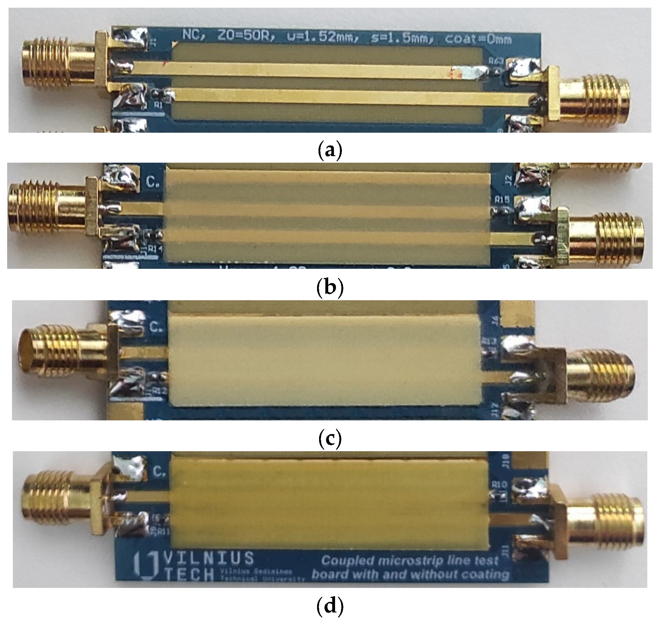
The fabricated DUT structures, featuring three coating layer thicknesses, are presented in Figure 3. These lines emulate a situation in which routed traces have undesired coupled lengths, thus leading to crosstalk. Figure 3a displays two independent 50 Ω lines without any coating layers and characterized by track widths of w0 = 1.52 mm and a spacing of s = 1.5 mm between the tracks. This structure serves as a reference for comparing the coated ones.
Subsequently, Figure 3b shows the structure with the line covered by coating layers of 0.1 mm thickness. To ensure a consistent 50 Ω impedance for this coupled line, the track width was reduced to 1.39 mm while maintaining the same spacing. Furthermore, Figure 3c represents the configuration with a 0.3 mm coating layer, whereas Figure 3d illustrates the structure with a 0.5 mm coating layer. In order to sustain a 50 Ω impedance for these coupled lines, the track widths of these structures were reduced to 1.3 mm and 1.25 mm while preserving the identical spacing of s = 1.5 mm between the tracks.
There are several reasons for using a wider instead of a narrow track:
- This approach clearly demonstrates that the overall width of the track with a certain target impedance (in this case, 50 Ω) has to be tweaked when adding laminate of a certain thickness above it.
- Wider tracks allow for less impedance mismatch due to etching tolerances, thus ensuring more precise measurement results. When the dielectric thickness between the track and the reference plane was around 0.15 mm and no coating layer was applied above, the 50 Ω traces had a width of around 0.3 mm. Therefore, a 5%–10% etching tolerance, ensured by the manufacturer, provides a more significant impedance shift in the case of narrow tracks as compared to the same for wider tracks.
Figure 4 presents a side-cut of a PCB with three different thicknesses of coating layers over the microstrip. As can be seen in Figure 3, the traces are only partially covered, and only those parts of the traces are coupled.
The investigation of the fabricated DUT boards was commenced by measuring time-domain reflectograms (TDR) of coupled lines without coating layers, which varied in width. The measurement setup is provided in Appendix A and shown in Figure A1. The results of these TDR responses are presented in Figure 5a. As observed from the graph, the reference coupled line with a track width of 1.5 mm exhibited an impedance of approximately 47.5 Ω, which deviated slightly from the desired value of 50 Ω during the design phase. This discrepancy arose due to the potential stack-up offsets introduced during the manufacturing process. Meanwhile, when measuring other coupled lines with track widths of 1.39 mm, 1.30 mm, and 1.25 mm, all at a fixed distance between the tracks (s = 1.5 mm), the obtained TDR responses demonstrated corresponding impedances of approximately 49 Ω, 52 Ω, and 54 Ω, respectively. This increase in impedance is attributed to the diminishing widths of the coupled lines. In the subsequent step, TDR plots were measured for the coupled lines with different coating layers. The results of these measurements are depicted in Figure 5b. As is evident from this graph, for all the coupled lines with diverse track widths and coating layers, the impedance remains virtually the same and aligns with the impedance of the reference coupled line. The measured TDR responses are not flat due to the short length of the PCB, whereas the impedance is a slightly off the target, Z0 = 50 Ω, but still within 10% tolerance because of the manufacturing process.
Upon analyzing the measurement results of the reflection coefficient, S11, as presented in Figure 6a, it can be concluded that the signal reflections across the entire 8 GHz frequency range are practically identical, with negligible differences in the obtained characteristics. This can be attributed to the fact that the impedance of all these coupled lines is close to 50 Ω.
In contrast, the results of the transmission coefficient S21 measurements, depicted in Figure 6b, demonstrate the significant effectiveness of the coating layers and a notable decrease in crosstalk. For instance, with a coating layer thickness of 0.1 mm, the crosstalk decreases by approximately 2–3 dB as compared to the reference within the frequency range up to 5 GHz. Similarly, with a coating layer thickness of 0.3 mm, the crosstalk decreases by approximately 5–6 dB. The most substantial reduction in crosstalk is observed when the coating layer thickness is 0.5 mm, resulting in a decrease of approximately 10 dB or more, which corresponds to the simulation results in Figure 1a. While increasing the thickness would further improve the results, approaching half of the PCB thickness or more becomes irrelevant in practice. The observed periodic dips in the S21 responses in Figure 1b and Figure 6b are due to the formation of standing waves in the DUT with the given parameters. As mentioned before, the coupled length is 38 mm, and λ/4 for 1 GHz with a dielectric permittivity equal to 4 is roughly 37.5 mm. Therefore, at a frequency of 1 GHz, the impedance in theory should be approaching infinity, and we see a dip in the S21 value, which is repeated periodically.
The average over-the-range crosstalk between the two microstrips with and without the coating layer approximation is shown in Figure 7. The S41 curves in Figure 1b and S21 curves in Figure 6b were obtained by subtracting the crosstalk results with certain coating thicknesses from the reference crosstalk at each point of the frequency range and then finding an average. According to the simulation results (blue line), crosstalk reduces exponentially (dashed line) and linearly increases the thickness of the coating, as shown in Figure 7. The simulated crosstalk approximation (blue solid line) is an average value for each coating layer thickness over the whole 8.5 GHz frequency range and correlates to the measurement results with less than 1 dB of difference, which is true to around 5 GHz. As can be seen in Figure 7, small resonances occur at frequencies above 5 GHz, which are valid for the presented DUT and can shift in other layouts.
Overall, a 0.1 mm coating layer does not sufficiently improve crosstalk, whereas the 0.5 mm layer provides a 10 dB crosstalk reduction, which can be beneficial in densely packed PCB layouts. Although coverlays can reduce crosstalk between traces, they also have disadvantages, including increased costs and reduced thermal performance of the PCB. This has to be taken into account when considering the implementation of coverlays as a means of reducing crosstalk.
4. Conclusions
Crosstalk presents a significant challenge when designing microstrip systems for modern high-density and high-speed PCBs. In such PCBs, traditional methods of widening the spacing between traces or introducing shielding to minimize crosstalk noise may prove less effective due to limited space. This paper suggests a direct and effective approach to minimize crosstalk by leveraging the coating (stiffener) layer commonly employed in rigid-flex PCB manufacturing. The proposal involves applying this layer to coat the microstrip lines, thereby reducing crosstalk. This paper describes the research on four microstrip line structures with various laminate thicknesses and with and without coating (stiffener). One structure had no coating layer and served as a reference with 50 Ω impedance. The other three structures had coating layers of 0.1 mm, 0.3 mm, and 0.5 mm, respectively. The widths of these structures were adjusted to maintain the impedance at 50 Ω, which was confirmed via TDR measurements. Based on the frequency-domain measurements of the S-parameters, it is evident that incorporating this coating layer (stiffener) results in a reduction in crosstalk exceeding 10 dB within the frequency range of up to 5 GHz. Moreover, a simplified approximation has been proposed, which shows good correlation with measurement results of up to 5 GHz, to evaluate the crosstalk reduction.
Author Contributions
All authors contributed to the present paper with the same effort in conceptualization, methodology, design, measurement, and writing the paper. All authors have read and agreed to the published version of the manuscript.
Funding
This research received no external funding.
Institutional Review Board Statement
Not applicable.
Informed Consent Statement
Not applicable.
Data Availability Statement
Not applicable.
Conflicts of Interest
The authors declare no conflict of interest.
Appendix A
The measurements and experimental analysis were conducted using a calibrated LA19-1304B Vector Network Analyzer (VNA) with an 8.5 GHz bandwidth, as shown in Figure A1.
Figure A1.
The experimental setup of the measurement test bench with LA19-1304B VNA.

To ensure accurate results, the fabricated DUT PCB was directly connected to the VNA, which eliminated the need for additional cables that could introduce insertion losses and unwanted reflections during the S11 and time-domain reflectometer (TDR) measurements. A 50 Ω calibration load was connected to the opposite end of the DUT coupled line to facilitate accurate S11 and TDR measurements. For the S21 response measurements, the DUT coupled line input was directly connected to the VNA, while the second end of the coupled line was connected to the VNA’s second port using a low-loss Sucoflex 126EA test lead/cable.
References
- Rajeswari, P.; Raju, S. Comparative Study of Crosstalk Reduction Techniques for Parallel Microstriplines. In Advances in Communication, Network, and Computing; Das, V.V., Stephen, J., Eds.; Lecture Notes of the Institute for Computer Sciences, Social Informatics and Telecommunications Engineering; Springer: Berlin/Heidelberg, Germany, 2012; Volume 108. [Google Scholar] [CrossRef]
- Wang, Y.; Li, C.; Li, X. Reducing Crosstalk Between Microstrip Lines Using CSR Structure. Authorea 2023, 1–10. [Google Scholar] [CrossRef]
- Cai, Q.-M.; Zhu, Y.; Zhang, R.; Ren, Y.; Ye, X.; Fan, J. A Study of Coverlay Coated Microstrip Lines for Crosstalk Reduction in DDR5. In Proceedings of the 2020 IEEE International Symposium on Electromagnetic Compatibility & Signal/Power Integrity (EMCSI), Reno, NV, USA, 27–31 July 2020; pp. 581–585. [Google Scholar] [CrossRef]
- Yu, X.-B.; Cai, Q.-M.; Ren, Y.; Ye, X.; Fan, J. Study of Thickening Soldermask Coated Microstrip Lines on High-Speed PCBs for Crosstalk Reduction in DDR5. In Proceedings of the 2020 IEEE International Symposium on Electromagnetic Compatibility & Signal/Power Integrity (EMCSI), Reno, NV, USA, 27–31 July 2020; pp. 575–577. [Google Scholar] [CrossRef]
- Deek, F.; Piket-May, M.; Bogatin, E. Novel low cost launch for measuring via-to-cavity coupling. In Proceedings of the 2021 IEEE Electrical Design of Advanced Packaging and Systems (EDAPS), Urbana, IL, USA, 13–15 December 2021; pp. 1–3. [Google Scholar] [CrossRef]
- Packianathan, R.; Srinivasan, R. Comparative Study of Crosstalk Reduction Techniques in RF Printed Circuit Board Using FDTD Method. Int. J. Antennas Propag. 2015, 2015, 294590. [Google Scholar] [CrossRef]
- Jiang, W.; Wang, J.; Zhao, L. A Novel Differential Microstrip Line Based on Spoof Surface Plasmon Polaritons. In Proceedings of the 2020 Cross Strait Radio Science & Wireless Technology Conference (CSRSWTC), Fuzhou, China, 13–16 December 2020; pp. 1–3. [Google Scholar] [CrossRef]
- Suntives, A.; Khajooeizadeh, A.; Abhari, R. Using via fences for crosstalk reduction in PCB circuits. In Proceedings of the 2006 IEEE International Symposium on Electromagnetic Compatibility, 2006. EMC 2006, Portland, OR, USA, 14–18 August 2006; pp. 34–37. [Google Scholar] [CrossRef]
- Ouyang, G.; Phan, L.-V.T.; Xiao, K. Methods to reduce crosstalk in flex circuit and PCB. In Proceedings of the 2016 IEEE International Symposium on Electromagnetic Compatibility (EMC), Ottawa, ON, Canada, 25–29 July 2016; pp. 25–28. [Google Scholar] [CrossRef]
- IPC-2141A; Design Guide for High-Speed Controlled Impedance Circuit Boards. IPC: Northbrook, IL, USA, 2004.
- Paul, C.R. Inductance Loop and Partial; Wiley: Hoboken, NJ, USA, 2010; p. 181. [Google Scholar]
- Paul, C.R. Analysis of Multiconductor Transmission Lines, 2nd ed.; Wiley: Hoboken, NJ, USA, 2008; pp. 146–147. [Google Scholar]
- Hammerstad, E.O.; Bekkadal, F. Microstrip Handbook; ELAB Report STF 44 A74169; The University of Trondheim: Trondheim, Norway, 1975. [Google Scholar]
- Wadell, B.C. Transmission Line Design Handbook; Artech House: Boston, MA, USA, 1991. [Google Scholar]
- Sierra Circuits. Embedded Microstrip Single Ended Impedance Calculator. Available online: https://impedance.app.protoexpress.com/?appid=EMSEIMPCAL (accessed on 13 September 2023).
Figure 1.
Crosstalk between two microstrips with and without coating layers: (a) schematic, (b) simulation results.
Figure 1.
Crosstalk between two microstrips with and without coating layers: (a) schematic, (b) simulation results.

Figure 2.
Two-layer PCB stack-up with a coating (stiffener) layer.

Figure 3.
Fabricated DUT boards with different coating layers: (a) 50 Ω coupled transmission lines without coating layers; (b) a 0.1 mm thick coating layer; (c) a 0.3 mm thick coating layer; (d) a 0.5 mm thick coating layer.
Figure 3.
Fabricated DUT boards with different coating layers: (a) 50 Ω coupled transmission lines without coating layers; (b) a 0.1 mm thick coating layer; (c) a 0.3 mm thick coating layer; (d) a 0.5 mm thick coating layer.

Figure 4.
Two-layer PCB stack-up side-cut with (a) 104 µm, (b) 317 µm, and (c) 480 µm coating (stiffener) layers.
Figure 4.
Two-layer PCB stack-up side-cut with (a) 104 µm, (b) 317 µm, and (c) 480 µm coating (stiffener) layers.

Figure 5.
TDR responses for coupled transmission lines: (a) without coating layers; (b) with coating layers.
Figure 5.
TDR responses for coupled transmission lines: (a) without coating layers; (b) with coating layers.

Figure 6.
Fabricated DUT board: (a) S11 and (b) S21 parameter measurement results.

Figure 7.
Average over-the-range crosstalk between two microstrips with and without coating layer approximation.
Figure 7.
Average over-the-range crosstalk between two microstrips with and without coating layer approximation.

Disclaimer/Publisher’s Note: The statements, opinions and data contained in all publications are solely those of the individual author(s) and contributor(s) and not of MDPI and/or the editor(s). MDPI and/or the editor(s) disclaim responsibility for any injury to people or property resulting from any ideas, methods, instructions or products referred to in the content. |
© 2023 by the authors. Licensee MDPI, Basel, Switzerland. This article is an open access article distributed under the terms and conditions of the Creative Commons Attribution (CC BY) license (https://creativecommons.org/licenses/by/4.0/).
Share and Cite
MDPI and ACS Style
Barzdenas, V.; Vasjanov, A. Crosstalk Reduction in High-Density Radio Frequency Printed Circuit Boards: Leveraging FR4 Coating Layers. Coatings 2023, 13, 1801. https://0-doi-org.brum.beds.ac.uk/10.3390/coatings13101801
AMA Style
Barzdenas V, Vasjanov A. Crosstalk Reduction in High-Density Radio Frequency Printed Circuit Boards: Leveraging FR4 Coating Layers. Coatings. 2023; 13(10):1801. https://0-doi-org.brum.beds.ac.uk/10.3390/coatings13101801
Chicago/Turabian StyleBarzdenas, Vaidotas, and Aleksandr Vasjanov. 2023. "Crosstalk Reduction in High-Density Radio Frequency Printed Circuit Boards: Leveraging FR4 Coating Layers" Coatings 13, no. 10: 1801. https://0-doi-org.brum.beds.ac.uk/10.3390/coatings13101801
Note that from the first issue of 2016, this journal uses article numbers instead of page numbers. See further details here.