
Atomic Layer Deposition for Tailoring Tamm Plasmon-Polariton with Ultra-High Accuracy
by
 and
and
Mantas Drazdys
1,
Ernesta Bužavaitė-Vertelienė
1,
Darija Astrauskytė
1 and
Zigmas Balevičius
1,2,* 1
Department of Laser Technologies, Center for Physical Sciences and Technology, 02300 Vilnius, Lithuania
2
Faculty of Electronics, Vilnius Gediminas Technical University, 10223 Vilnius, Lithuania
*
Author to whom correspondence should be addressed.
Coatings 2024, 14(1), 33; https://0-doi-org.brum.beds.ac.uk/10.3390/coatings14010033
Submission received: 1 December 2023
/
Revised: 22 December 2023
/
Accepted: 24 December 2023
/
Published: 26 December 2023
(This article belongs to the Special Issue Fabrication of Plasmonic Thin Films, Their Characterization and Applications)
Abstract
:In this study, we demonstrate the potential capability to control Tamm plasmon-polaritons (TPP) by applying atomic layer deposition (ALD) as a highly precise technique for plasmonic applications. Applications in plasmonics usually require tens of nanometers or less thick layers; thus, ALD is a very suitable technique with monolayer-by-monolayer growth of angstrom resolution. Spectroscopic ellipsometry and polarized reflection intensity identified the TPP resonances in the photonic band gap (PBG) formed by periodically alternating silicon oxide and tantalum oxide layers. The sub-nanometer control of the Al2O3 layer by ALD allows precise tailoring of TPP resonances within a few nanometers of spectral shift. The employing of the ALD method for the fabrication of thin layers with sub-nanometer thickness accuracy in more complex structures proves to be a versatile platform for practical applications where tunable plasmonic resonances of high quality are required.
1. Introduction
During the last decade, much attention has been given to photonic crystal (PC) structures covered with a thin metal layer on top of PC [1,2]. A type of surface mode can be generated in PC-metal structures, the so-called TPP, appearing at the boundary between the PC and the metal layer [3,4]. TPPs are optical states, which are similar to the electron states proposed by I. Tamm [5] and can occur in the energy band gap at a crystal surface. These energy band gap regions are the stop band of the PCs due to the Bragg reflections in the periodic structure. In contrast to the surface plasmon-polariton (SPP)-propagated surface electromagnetic waves (SEW), the TPPs are non-propagating states and can be excited in both p- and s-polarizations, like the Bloch surface waves. In fact, the TPP is a standing wave, which is an interference phenomenon of two SEWs propagating in opposite directions [3,6]. TPPs have an in-plane wave vector that is less than the wave vector of light in a vacuum, which allows for their direct optical excitation, while for the SPPs to achieve a total internal reflection condition, the incident light must reach an in-plane wave vector equal to the surface plasmon resonance [4].
The distinct optical dispersion properties of TPPs, compared with SPP, lead to more simple optical configurations without additional couplers (prisms or gratings). This opens new possibilities for various applications such as optical biosensors [7,8,9,10], bandgap filters [11,12], nanolasing [13,14], and others [15,16,17,18,19,20,21,22]. For further technological progress in these applications, precise tuning of the optical properties of the TPP-based nanostructures as well as the plasmonic resonance position in the spectra is necessary. For this purpose, a thin film deposition technique with high resolution is needed. For structures with Bragg mirrors in the visible wavelength range, usually the ion beam sputtering (IBS) deposition technique is used as well as thermal evaporation or magnetron sputtering for the fabrication of thin metal layers. These methods work rather well; however, in order to control deposited layer thickness in the angstrom range, other techniques should be used. In this case, ALD is a type of chemical vapor deposition (CVD) technique with monolayer-by-monolayer growth of angstrom resolution [23,24,25]. This deposition technique is widely used in the microelectronics industry [26,27,28]. Also, ALD is used for the modification of various surfaces and for the protection and encapsulation of nanostructures [29,30,31]. In ALD, the desired thickness can be controlled by depositing a required number of cycles, resulting in atomically thick layers. It should be noted that the film thickness can be precisely controlled by the large area due to self-saturating and self-limiting growth mechanisms. It is important to maintain efficient purge times and temperatures to ensure energy and cost-efficient deposition on the surface. During the deposition process, precursors do not mix with each other, so chemical reactions occur only on the surface. The separate injection of precursors allows for the use of highly reactive precursors, which is difficult to achieve in other CVD-based methods, and reactions occur at relatively low temperatures (about 50–250 °C); however, the ALD deposition rate is slow compared with other methods, especially when dealing with hundreds of nanometer-thick layers, making it ideal for ultra-thin layers in complex nanostructures. Fortunately, applications in plasmonics usually require tens of nanometer-thick layers, so the fabrication time is significantly reduced compared to thick structures.
In this study, we demonstrate the potential capability to control TPP by applying ALD as a highly precise technique for plasmonic applications. The TPP resonance dependence on Al2O3 layer thickness was evaluated, where 3 nm of Al2O3 layer thickness difference corresponded to ≈3 nm shift of TPP minima, showing precise control capabilities when the ALD method is used.
2. Materials and Methods
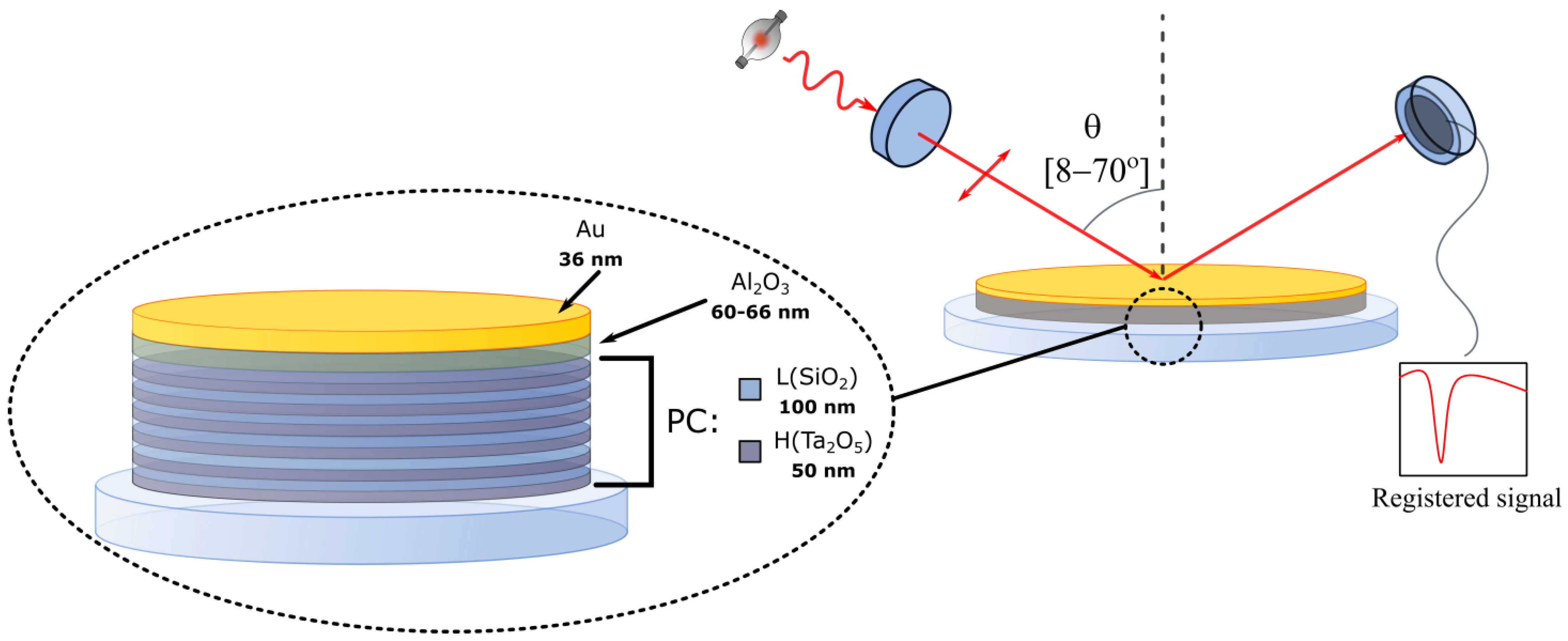
The structure of the investigated samples consisted of a Bragg reflector, an Al2O3 layer, and a gold layer (Figure 1), all deposited on fused silica (FS) glass substrates. The Bragg reflector (1D PC) consisted of 12 alternating high (Ta2O5) (marked as H in Figure 1) and low (SiO2) (marked as L in Figure 1) refractive index materials, where Ta2O5 thickness was 50 nm and SiO2 thickness was 100 nm. Three samples with varying Al2O3 layer thicknesses (60 nm, 63 nm, and 66 nm) were investigated.
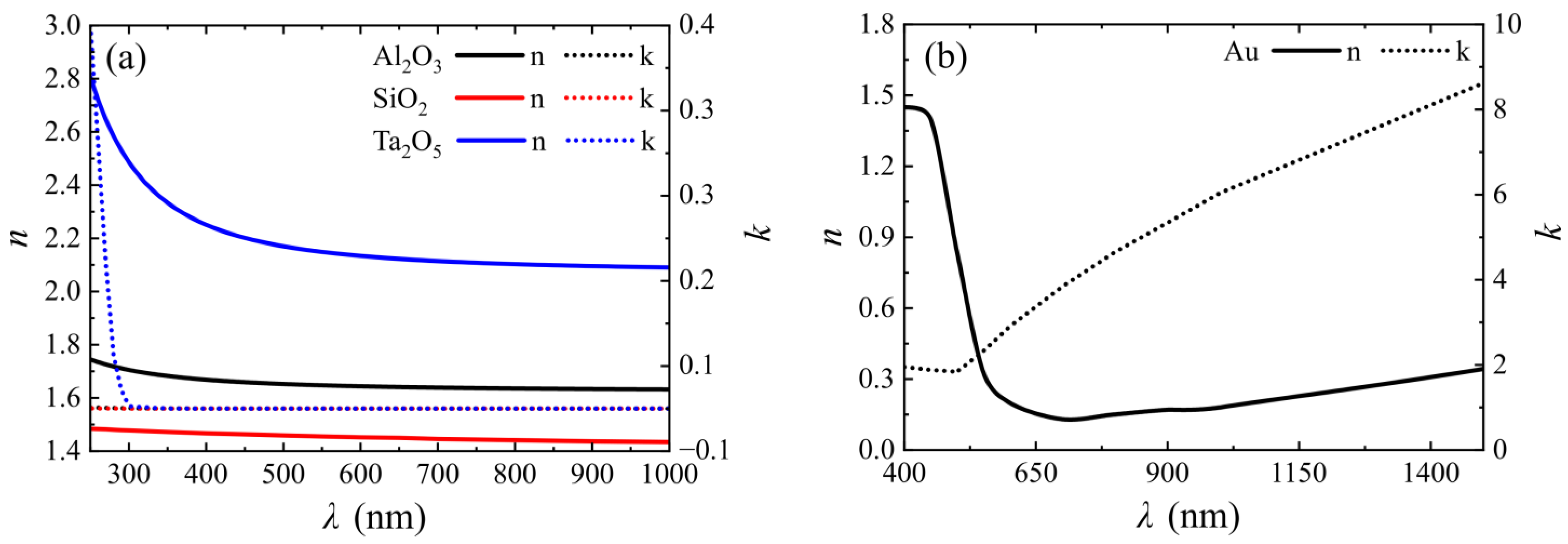
First, the structure of PC/Al2O3/Au was modeled using TFCalc v3.5.15 software with different Al2O3 layers (60 nm, 63 nm, and 66 nm). The refractive indexes and extinction coefficients of Ta2O5, Al2O3, and SiO2 for the model were experimentally obtained and can be seen in Figure 2a. Gold data was obtained from the literature (Figure 2b) [32].
The Bragg reflector consisted of 6 bilayers of ≈50 nm Ta2O5/≈100 nm SiO2 and was deposited using ion beam sputtering (IBS) technology (Navigator, Cutting Edge Coatings, Hanover, Germany). Ta2O5 and SiO2 were deposited by sputtering Ta and Si targets, respectively, using a radio-frequency argon ion source. During the process, oxygen gas was fed near the substrates to ensure complete oxidation of the coating. The sputtering process was performed at a temperature of ≈50 °C. The thickness of each layer was controlled by broadband optical monitoring (BBOM).
The Al2O3 layer was deposited using ALD technology (Savannah S200, Veeco, Plainview, NY, USA). The layer was grown using trimethylaluminium (TMA) as an Al precursor and water as an oxygen source. During the deposition, the reactor temperature was kept at 150 °C, and a 30 sccm flow of nitrogen gas was used as purging and carrier gas. Deposition cycles consisted of four steps: a 0.02 s TMA pulse, a 6 s purge, a 0.02 s water pulse, and a 6 s purge. To achieve Al2O3 layers of varying thickness, three samples with a Bragg reflector were placed into the reactor, and 600 cycles of Al2O3 were deposited, resulting in a 60 nm thickness. After removing one sample from the reactor, an additional 30 cycles of Al2O3 were deposited, resulting in a final Al2O3 layer thickness of 63 nm. After removing one more sample and depositing 30 more cycles, the thickness of the final sample with the Al2O3 layer was 66 nm.
The 36 nm gold layer was deposited using magnetron sputtering (MS) technology (Q150T ES, Quorum, Nottingham, UK). The gold film was sputtered from the gold target using argon gas at room temperature. Due to the small dimensions of the chamber, samples were placed in the chamber and coated one by one.
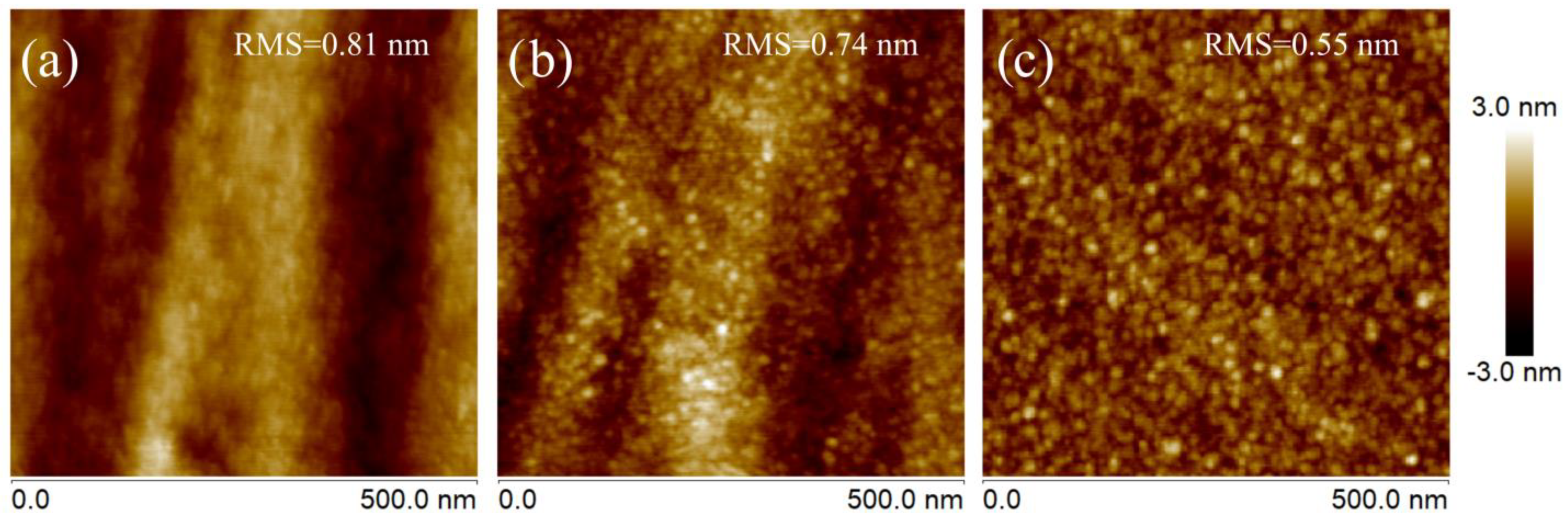
The surface morphology of the Bragg reflector deposited by IBS and the complete structure fabricated using ALD and magnetron sputtering were characterized by atomic force microscopy (AFM) (Figure 3). Five different 500 nm × 500 nm areas of a sample were scanned, and the root mean square (RMS) roughness of the samples was determined using NanoScope Analysis 1.40 software. Averaged RMS values and calculated relative errors are presented in Figure 3. The surface morphology results have shown that the surface roughness of the Bragg mirror’s last layer was 0.81 ± 0.08 nm. After deposition of the Al2O3 layer by ALD, the surface roughness slightly decreased to 0.74 ± 0.07 nm but stayed within the error limit, and further sputtering of the thin gold layer also decreased the RMS to 0.55 ± 0.09 nm. As mentioned above, TPP optical states form at the inner interface between gold and aluminum oxide; thus, the main influence on such surface resonances would be from the roughness of the ALD-fabricated layer.
Variable angle spectroscopic ellipsometry (VASE) measurements were conducted using a dual rotating compensator ellipsometer RC2 (J. A. Woollam Co., Lincoln, NE, USA) in a 210–1700 nm spectral range and at an angle of incidence (AOI) range of 20–70 deg.
Additionally, the reflection spectra of the Bragg reflector, the Bragg reflector with an Al2O3 layer, and the final structure (Bragg reflector/Al2O3/Au) were measured with the PhotonRT spectrometer (Essent Optics, Liasny, Belarus). Spectra were measured at a small AOI of 8 deg., which is not accessible with ellipsometry, and in a spectral range of λ = 350–900 nm.
3. Results and Discussion
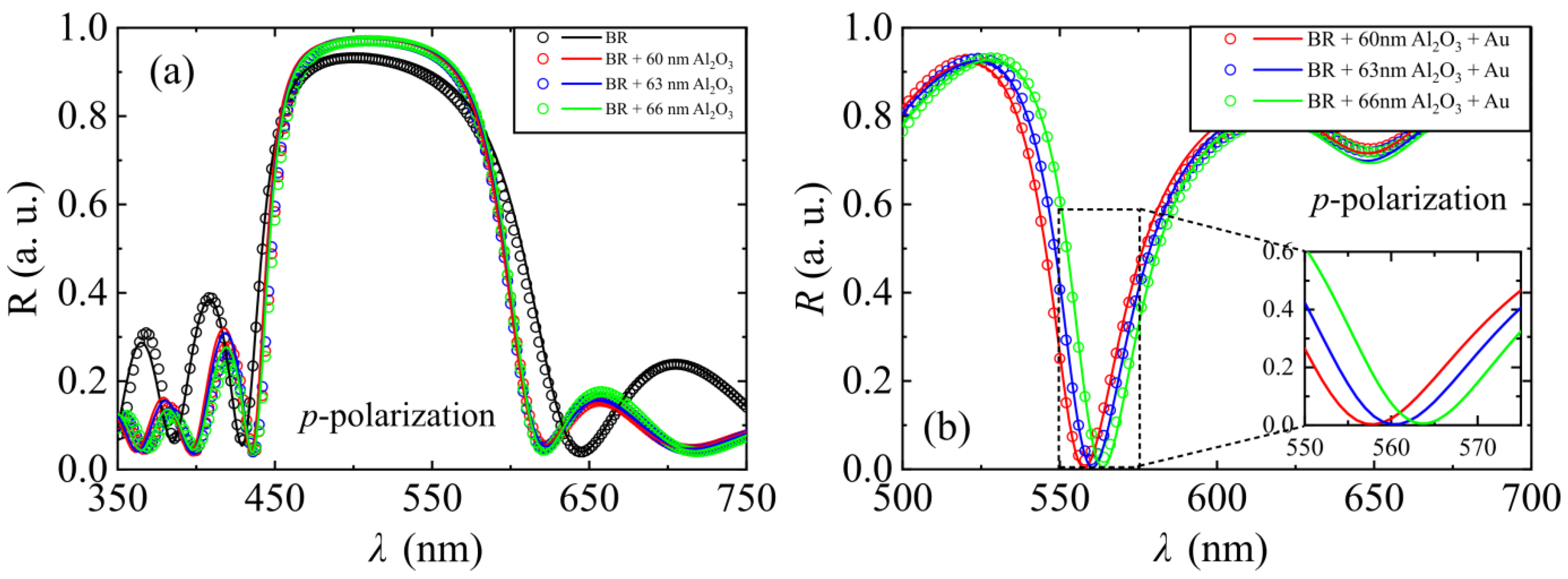
It has been shown before that the thickness of the last layer in the 1D PC can easily be used for tuning the TPP dip in the photonic stop band during the fabrication process. However, precise control of the thickness during the fabrication is crucial for the spectral position of the plasmonic dip, as it is very sensitive to the inner interface between metal and the dielectric layer. In order to fabricate the plasmonic-photonic nanostructures with TPP dip at a few nanometers tuning position, the spectra modeling of such nanostructures was performed to evaluate the optimized optical parameters (thickness and optical dispersions) of the structure. The simulations reveal that in order to reliably control the TPP dip in the spectra with nanometer resolution, the thickness control during the fabrication process for the 1D PC should be less than 1 nm. Such resolution is available for the ALD method compared with the usually used IBS method for such dielectric structures, where thickness control is between 3 and 8 nm [24,33]. The three samples were simulated with only one difference in the thickness of the Bragg reflector’s last layers. The aluminum oxide varied by 3 nm for each sample: 60 nm, 63 nm, and 66 nm, respectively. Such a difference in simulation gave a 3 nm red shift of the TPP dip in the reflectance spectra. However, the fabrication time for ALD is much longer for the deposition of tens or hundreds of nanometers, which are necessary for such photonic structures.
For optimization of the process, it is reasonable to combine both IBS and ALD methods: the main “bulk” Bragg reflector part consisting of 6 bilayers of HL refractive index dielectrics was produced by using IBS; meanwhile, the last aluminum oxide layer, for which sub-nanometer thickness control is essential, was deposited by the ALD method; and further, magnetron sputtering was used for gold layer deposition. As the IBS deposition method is based on high-energy ions hitting the material target and part of the material being sputtered and later condensed on the substrate, this method has been proven to be a reliable tool for the fabrication of hundreds of nanometer-thick multilayer structures with good quality for optical purposes [34,35]. However, the fast deposition rate, compared with the ALD method, does not allow sub-nanometer thickness control of the layers. Meanwhile, the ALD method, characterized by self-limiting surface reactions, gives the possibility of controlling the thickness of the layer by the number of atomically thick cycles [23,24]. This property is particularly suitable for plasmonic-based nanostructures, where often less than 10 nm dielectric spacers are used and precise control of the single layer thickness is necessary [24].
This study was focused on demonstrating the application of ALD for fine-tuning the wavelength of TPP modes. In order to generate the TPP, a structure consisting of PC and a metallic layer is needed. In this case, the PC consisted of a Bragg reflector with a single Al2O3 layer on top. The spectrum of an IBS-deposited Bragg reflector without an Al2O3 layer is depicted in Figure 4a (black dots). To ensure high precision of thicknesses of Al2O3 layers, they were deposited using ALD (Figure 4a (red, blue, and green dots for 60 nm, 63 nm, and 66 nm Al2O3 thickness, respectively)). After deposition of the Al2O3 layer, the PBG reduces from 162 nm (Bragg reflector) to 147 nm at full width at half maximum (FWHM), while the reflection increases from 93% to 97%. The exact thickness values of deposited Al2O3 were predicted by the number of cycles in the ALD process, which allows us to presume the deposited thickness of Al2O3. Moreover, after the deposition of the metallic layer, which in this case was a gold layer, on PCs with different Al2O3 thicknesses, structures generating TPP mode at different wavelengths were achieved (Figure 4b reflection spectra at 8 deg. AOI), which increased the thickness accuracy of Al2O3 layers. Structures with Al2O3 thicknesses of 60 nm, 63 nm, and 66 nm led to TPP mode being generated at λ = 558 nm, λ = 561 nm, and λ = 564 nm, respectively, which fits well with modeling results. The modeling of plasmonic-photonic nanostructure was performed using TFCalcTM v3.5.15 software by slide-tuning the thickness of the layers, resulting in the thickness of 6 Ta2O5 and SiO2 bilayers at 50.6 nm and 101.3 nm, respectively, and 61.3 nm/63.3 nm/66.3 nm Al2O3 with 36.0 nm Au on top. The good agreement between experimental and modeled results demonstrates how precisely the ALD method allows for the control of thickness. The wavelength shift of TPP resonance was equal to 3 nm ± 1 nm and 4 nm ± 1 nm for the Al2O3 thickness difference of 2 nm (61.3 nm–63.3 nm) and 3 nm (63.3 nm–66.3 nm), respectively. The modeling and experimental results demonstrate linear TPP resonant wavelength dependence on Al2O3 layer thickness, thus showing how the ALD method allows for easy estimation of the parameters required to achieve precise TPP frequency.
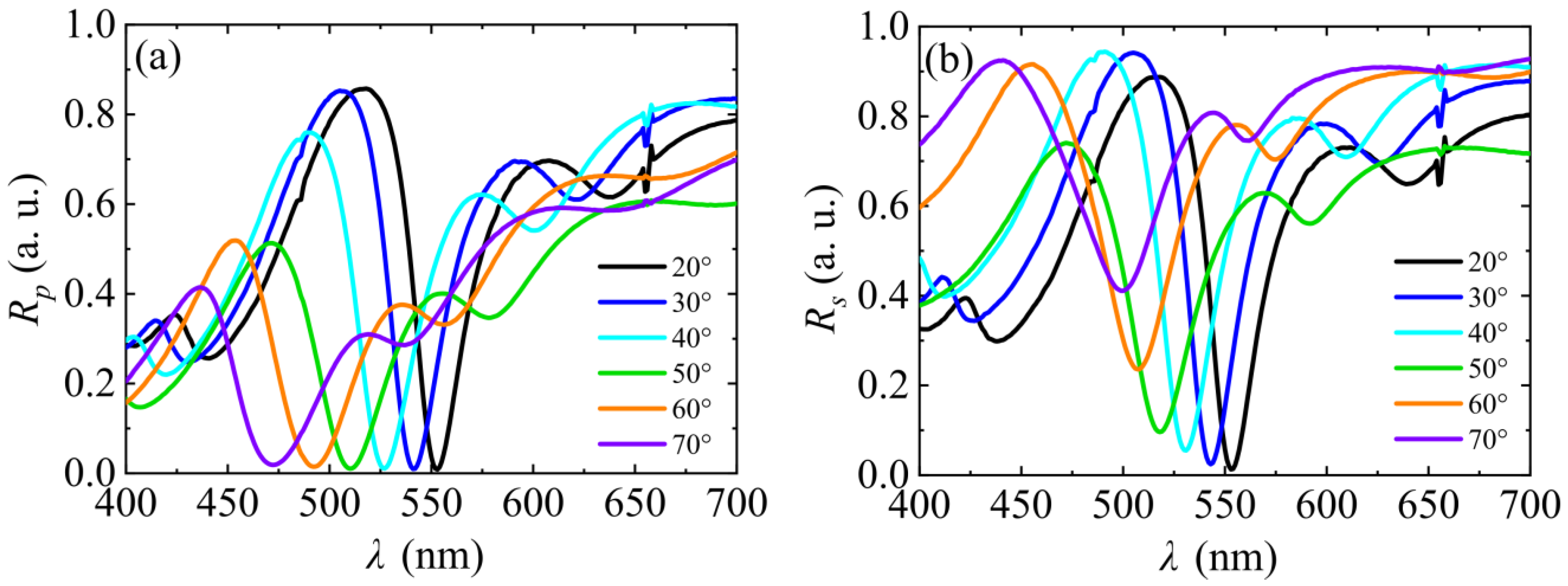
Variable-angle spectroscopic ellipsometry (VASE) was used for full optical response characterization of the three samples. The VASE method allows to measure ellipsometric parameters Ψ(λ) and Δ(λ) in a wide-angle range. Based on these measurements of the p- and s-polarized reflectance intensity (Figure 5), the behavior of TPP mode in both polarization components can be evaluated. At small AOI, the TPP p- and s-polarization components are close in the spectrum, gradually becoming more spectrally separated with increasing angle. At 20 deg AOI, the TPP of both p- and s-component minima is at 553 nm, while at 70 deg AOI, the TPP resonance shifts to 472 nm and 499 nm for p- and s-polarizations, respectively. This feature can be useful in various applications as both p- and s-components of the TPP can be used as probes (e.g., two separate probes (wavelengths) for optical sensors).
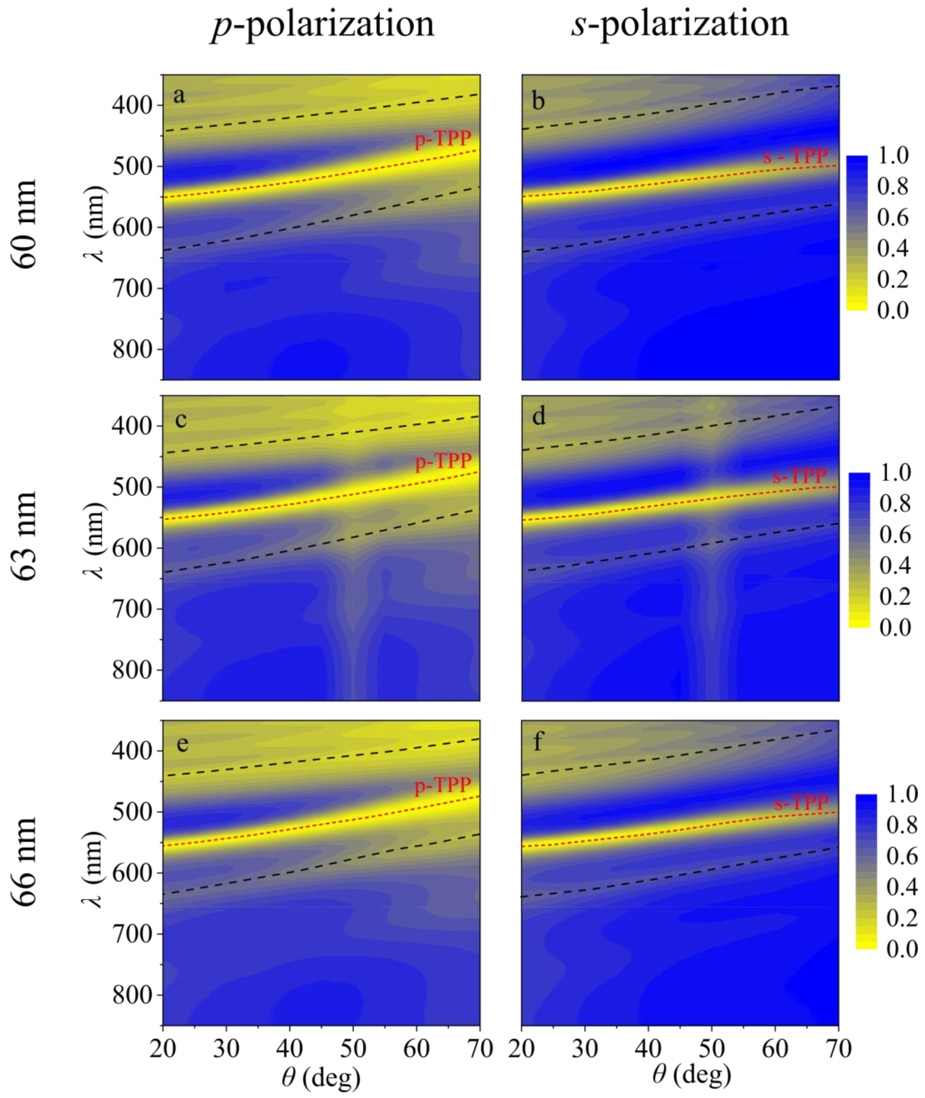
The VASE measurements allow for the analysis of the optical dispersion maps of the TPP in p- and s-polarized reflectance (Figure 6). It can be seen that TPP excitation has parabolic dispersion, with the p-polarized component shifting more towards shorter wavelengths as AOI increases compared with the s-polarization TPP component. In these maps, the dispersion line of the TPP can be clearly seen shifting from 550 nm at 20 deg. AOI for both p- and s-polarized components to 470 nm (p-polarization) and 500 nm (s-polarization) at 70 degrees (Figure 6a,b). The width of the PBG for the p-component of TPP decreased with increasing AOI by ≈40 nm, while the s-polarization PBG width narrowed by less than 10 nm. The width of TPP dispersion lines broadened less for s-polarization, as this component weakly depends on the AOI (the vector is in the plane of the sample surface). By comparing the quality factor Q for both TPP components, it was determined that the Q for 20 deg. AOI was equal to 21.19 for both p- and s-components, while at 70 deg. AOI, the Q was 9.25 and 11.86 for the p- and s-polarization components, respectively. This shows that better TPP resonance quality at large AOI can be achieved in s-polarization. However, the miniscule differences between the samples with various aluminum oxide last layers were better seen in the spectra with separate AOIs (Figure 4). As could be seen from Figure 4, the dips of TPP were shifted in the spectra by ≈3 nm for each sample with a thicker aluminum oxide layer. It is reasonable to assume that all three samples had an equal thickness change of 3 nm because Tamm plasmon resonances were placed for an equal shift in the wavelength spectra. Moreover, it is well known that plasmonic resonances have a linear dependence on the optical thickness of dielectric material. The increasing thickness of Al2O3 from 60 nm to 66 nm resulted in decreased FWHM from 26.3 nm to 24.6 nm, respectively, and the quality factor Q increased with larger Al2O3 thickness: Q60 = 21.1, Q63 = 21.6, and Q66 = 22.36.
4. Conclusions
In this study, we demonstrate that the ALD method allows for the precise tailoring of Tamm plasmonic resonances with high accuracy on a few nanometer-thickness scales. Moreover, the ALD method exhibits the capability to finely tune layers to sub-nanometer thickness. Spectroscopic ellipsometry and polarized reflection intensity at small AOI identified the TPP resonances in the PBG formed by periodically alternating silicon oxide and tantalum oxide layers. The modeling of the optical response of such plasmonic-photonic structures has shown that they fit reasonably well with experimentally measured polarized reflectance spectra. The employing of the ALD method for the fabrication of thin layers with sub-nanometer thickness accuracy in more complex structures proves to be a versatile platform for practical applications where tunable plasmonic resonances of high quality are required.
Author Contributions
Conceptualization, Z.B. and M.D.; methodology, M.D. and E.B.-V.; formal analysis, M.D., E.B.-V., D.A. and Z.B.; investigation, M.D., E.B.-V., D.A. and Z.B.; writing—original draft preparation, M.D.; writing—review and editing, M.D., Z.B. and E.B.-V.; visualization, M.D.; supervision, Z.B. All authors have read and agreed to the published version of the manuscript.
Funding
This research received no external funding.
Institutional Review Board Statement
Not applicable.
Informed Consent Statement
Not applicable.
Data Availability Statement
Data are contained within the article.
Conflicts of Interest
The authors declare no conflict of interest.
References
- Afinogenov, B.I.; Bessonov, V.O.; Nikulin, A.A.; Fedyanin, A.A. Observation of Hybrid State of Tamm and Surface Plasmon-Polaritons in One-Dimensional Photonic Crystals. Appl. Phys. Lett. 2013, 103, 061112. [Google Scholar] [CrossRef]
- Bužavaitė-Vertelienė, E.; Vertelis, V.; Balevičius, Z. The Experimental Evidence of a Strong Coupling Regime in the Hybrid Tamm Plasmon-Surface Plasmon Polariton Mode. Nanophotonics 2021, 10, 1565–1571. [Google Scholar] [CrossRef]
- Kaliteevski, M.; Iorsh, I.; Brand, S.; Abram, R.A.; Chamberlain, J.M.; Kavokin, A.V.; Shelykh, I.A. Tamm Plasmon-Polaritons: Possible Electromagnetic States at the Interface of a Metal and a Dielectric Bragg Mirror. Phys. Rev. B 2007, 76, 165415. [Google Scholar] [CrossRef]
- Sasin, M.E.; Seisyan, R.P.; Kalitteevski, M.A.; Brand, S.; Abram, R.A.; Chamberlain, J.M.; Egorov, A.Y.; Vasil’ev, A.P.; Mikhrin, V.S.; Kavokin, A.V. Tamm Plasmon Polaritons: Slow and Spatially Compact Light. Appl. Phys. Lett. 2008, 92, 251112. [Google Scholar] [CrossRef]
- Tamm, I. Über eine mögliche Art der Elektronenbindung an Kristalloberflächen. Z. Phys. 1932, 76, 849–850. [Google Scholar] [CrossRef]
- Vinogradov, A.P.; Dorofeenko, A.V.; Erokhin, S.G.; Inoue, M.; Lisyansky, A.A.; Merzlikin, A.M.; Granovsky, A.B. Surface State Peculiarities in One-Dimensional Photonic Crystal Interfaces. Phys. Rev. B 2006, 74, 045128. [Google Scholar] [CrossRef]
- Bittrich, E.; Rodenhausen, K.B.; Eichhorn, K.-J.; Hofmann, T.; Schubert, M.; Stamm, M.; Uhlmann, P. Protein Adsorption on and Swelling of Polyelectrolyte Brushes: A Simultaneous Ellipsometry-Quartz Crystal Microbalance Study. Biointerphases 2010, 5, 159–167. [Google Scholar] [CrossRef] [PubMed]
- Balevičius, Z. Strong Coupling between Tamm and Surface Plasmons for Advanced Optical Bio-Sensing. Coatings 2020, 10, 1187. [Google Scholar] [CrossRef]
- Plikusienė, I.; Bužavaitė-Vertelienė, E.; Mačiulis, V.; Valavičius, A.; Ramanavičienė, A.; Balevičius, Z. Application of Tamm Plasmon Polaritons and Cavity Modes for Biosensing in the Combined Spectroscopic Ellipsometry and Quartz Crystal Microbalance Method. Biosensors 2021, 11, 501. [Google Scholar] [CrossRef]
- Anulytė, J.; Bužavaitė-Vertelienė, E.; Stankevičius, E.; Vilkevičius, K.; Balevičius, Z. High Spectral Sensitivity of Strongly Coupled Hybrid Tamm-Plasmonic Resonances for Biosensing Application. Sensors 2022, 22, 9453. [Google Scholar] [CrossRef]
- Ferrier, L.; Nguyen, H.S.; Jamois, C.; Berguiga, L.; Symonds, C.; Bellessa, J.; Benyattou, T. Tamm Plasmon Photonic Crystals: From Bandgap Engineering to Defect Cavity. APL Photonics 2019, 4, 106101. [Google Scholar] [CrossRef]
- Liu, Q.; Zhao, X.; Li, C.; Zhou, X.; Chen, Y.; Wang, S.; Lu, W. Coupled Tamm Plasmon Polaritons Induced Narrow Bandpass Filter with Ultra-Wide Stopband. Nano Res. 2022, 15, 4563–4568. [Google Scholar] [CrossRef]
- Symonds, C.; Lheureux, G.; Hugonin, J.P.; Greffet, J.J.; Laverdant, J.; Brucoli, G.; Lemaitre, A.; Senellart, P.; Bellessa, J. Confined Tamm Plasmon Lasers. Nano Lett. 2013, 13, 3179–3184. [Google Scholar] [CrossRef] [PubMed]
- Lheureux, G.; Azzini, S.; Symonds, C.; Senellart, P.; Lemaître, A.; Sauvan, C.; Hugonin, J.-P.; Greffet, J.-J.; Bellessa, J. Polarization-Controlled Confined Tamm Plasmon Lasers. ACS Photonics 2015, 2, 842–848. [Google Scholar] [CrossRef]
- Auguié, B.; Fuertes, M.C.; Angelomé, P.C.; Abdala, N.L.; Soler Illia, G.J.A.A.; Fainstein, A. Tamm Plasmon Resonance in Mesoporous Multilayers: Toward a Sensing Application. ACS Photonics 2014, 1, 775–780. [Google Scholar] [CrossRef]
- Huang, S.-G.; Chen, K.-P.; Jeng, S.-C. Phase Sensitive Sensor on Tamm Plasmon Devices. Opt. Mater. Express 2017, 7, 1267. [Google Scholar] [CrossRef]
- Maji, P.S.; Das, R. Hybrid-Tamm-Plasmon-Polariton Based Self-Reference Temperature Sensor. J. Light. Technol. 2017, 35, 2833–2839. [Google Scholar] [CrossRef]
- Paulauskas, A.; Tumenas, S.; Selskis, A.; Tolenis, T.; Valavicius, A.; Balevicius, Z. Hybrid Tamm-Surface Plasmon Polaritons Mode for Detection of Mercury Adsorption on 1D Photonic Crystal/Gold Nanostructures by Total Internal Reflection Ellipsometry. Opt. Express 2018, 26, 30400. [Google Scholar] [CrossRef]
- Buchnev, O.; Belosludtsev, A.; Reshetnyak, V.; Evans, D.R.; Fedotov, V.A. Observing and Controlling a Tamm Plasmon at the Interface with a Metasurface. Nanophotonics 2020, 9, 897–903. [Google Scholar] [CrossRef]
- Buzavaite-Verteliene, E.; Valavicius, A.; Grineviciute, L.; Tolenis, T.; Lukose, R.; Niaura, G.; Balevicius, Z. Influence of the Graphene Layer on the Strong Coupling in the Hybrid Tamm-Plasmon Polariton Mode. Opt. Express 2020, 28, 10308. [Google Scholar] [CrossRef]
- Anulytė, J.; Bužavaitė-Vertelienė, E.; Vertelis, V.; Stankevičius, E.; Vilkevičius, K.; Balevičius, Z. Influence of a Gold Nano-Bumps Surface Lattice Array on the Propagation Length of Strongly Coupled Tamm and Surface Plasmon Polaritons. J. Mater. Chem. C 2022, 10, 13234–13241. [Google Scholar] [CrossRef]
- Kar, C.; Jena, S.; Udupa, D.V.; Rao, K.D. Tamm plasmon polariton in planar structures: A brief overview and applications. Opt. Laser Technol. 2023, 159, 108928. [Google Scholar] [CrossRef]
- George, S.M. Atomic Layer Deposition: An Overview. Chem. Rev. 2010, 110, 111–131. [Google Scholar] [CrossRef] [PubMed]
- Im, H.; Wittenberg, N.J.; Lindquist, N.C.; Oh, S.-H. Atomic Layer Deposition: A Versatile Technique for Plasmonics and Nanobiotechnology. J. Mater. Res. 2012, 27, 663–671. [Google Scholar] [CrossRef] [PubMed]
- Marichy, C.; Bechelany, M.; Pinna, N. Atomic Layer Deposition of Nanostructured Materials for Energy and Environmental Applications. Adv. Mater. 2012, 24, 1017–1032. [Google Scholar] [CrossRef]
- Mistry, K.; Chau, R.; Choi, C.-H.; Ding, G.; Fischer, K.; Ghani, T.; Grover, R.; Han, W.; Hanken, D.; Hattendorf, M.; et al. A 45nm Logic Technology with High-k+Metal Gate Transistors, Strained Silicon, 9 Cu Interconnect Layers, 193nm Dry Patterning, and 100% Pb-Free Packaging. In Proceedings of the 2007 IEEE International Electron Devices Meeting, Washington, DC, USA, 10–12 December 2007; pp. 247–250. [Google Scholar]
- Ye, P.D. Main Determinants for III–V Metal-Oxide-Semiconductor Field-Effect Transistors (Invited). J. Vac. Sci. Technol. A 2008, 26, 697–704. [Google Scholar] [CrossRef]
- Siddiqi, M.A.; Siddiqui, R.A.; Atakan, B.; Roth, N.; Lang, H. Thermal Stability and Sublimation Pressures of Some Ruthenocene Compounds. Materials 2010, 3, 1172–1185. [Google Scholar] [CrossRef]
- Li, Y.; Xiong, Y.; Yang, H.; Cao, K.; Chen, R. Thin Film Encapsulation for the Organic Light-Emitting Diodes Display via Atomic Layer Deposition. J. Mater. Res. 2020, 35, 681–700. [Google Scholar] [CrossRef]
- Wang, H.; Zhao, Y.; Wang, Z.; Liu, Y.; Zhao, Z.; Xu, G.; Han, T.-H.; Lee, J.-W.; Chen, C.; Bao, D.; et al. Hermetic Seal for Perovskite Solar Cells: An Improved Plasma Enhanced Atomic Layer Deposition Encapsulation. Nano Energy 2020, 69, 104375. [Google Scholar] [CrossRef]
- Cao, K.; Cai, J.; Shan, B.; Chen, R. Surface Functionalization on Nanoparticles via Atomic Layer Deposition. Sci. Bull. 2020, 65, 678–688. [Google Scholar] [CrossRef]
- Johnson, P.B.; Christy, R.W. Optical Constants of the Noble Metals. Phys. Rev. B 1972, 6, 4370–4379. [Google Scholar] [CrossRef]
- Ristau, D.; Gross, T. Ion Beam Sputter Coatings for Laser Technology. In Advances in Optical Thin Films II; Amra, C., Kaiser, N., Macleod, H.A., Eds.; SPIE: Jena, Germany, 2005; Volume 5963, p. 596313. [Google Scholar]
- Amato, A.; Terreni, S.; Dolique, V.; Forest, D.; Gemme, G.; Granata, M.; Mereni, L.; Michel, C.; Pinard, L.; Sassolas, B.; et al. Optical Properties of High-Quality Oxide Coating Materials Used in Gravitational-Wave Advanced Detectors. J. Phys. Mater. 2019, 2, 035004. [Google Scholar] [CrossRef]
- Sakiew, W.; Schrameyer, S.; Schwerdtner, P.; Erhart, N.; Starke, K. Large Area Precision Optical Coatings by Reactive Ion Beam Sputtering. Appl. Opt. 2020, 59, 4296. [Google Scholar] [CrossRef] [PubMed]
Figure 1.
The TPP excitation optical configuration (right) and structure of the investigated samples (left). The letters L and H (left side of the figure) indicate the low and index of refraction, respectively.
Figure 1.
The TPP excitation optical configuration (right) and structure of the investigated samples (left). The letters L and H (left side of the figure) indicate the low and index of refraction, respectively.

Figure 2.
Refractive indexes (solid curves) and extinction coefficients (dotted curves) of materials used in the structure model: (a) Al2O3 (black curve), SiO2 (red curve), Ta2O5 (blue curve), and (b) Au.
Figure 2.
Refractive indexes (solid curves) and extinction coefficients (dotted curves) of materials used in the structure model: (a) Al2O3 (black curve), SiO2 (red curve), Ta2O5 (blue curve), and (b) Au.

Figure 3.
The surface of structures (a) Bragg reflector on FS, (b) Bragg reflector on FS + Al2O3, and (c) Bragg reflector on FS + Al2O3 + Au is characterized by AFM.
Figure 3.
The surface of structures (a) Bragg reflector on FS, (b) Bragg reflector on FS + Al2O3, and (c) Bragg reflector on FS + Al2O3 + Au is characterized by AFM.

Figure 4.
Experimentally measured (circles) and simulated (solid line) reflectance at 8 deg. AOI: (a) IBS-deposited Bragg reflector coating (black), with different thicknesses of atomic-layer-deposited Al2O3: 60 nm (red), 63 nm (blue), and 66 nm (green). (b) MS-deposited Au film on Bragg reflector + Al2O3 stacks with different Al2O3 thicknesses: 60 nm (red), 63 nm (blue), and 66 nm (green).

Figure 5.
Experimental spectra of (a) p-intensity and (b) s-intensity dependence on the AOI for Bragg reflector + 63 nm Al2O3 + Au stack.
Figure 5.
Experimental spectra of (a) p-intensity and (b) s-intensity dependence on the AOI for Bragg reflector + 63 nm Al2O3 + Au stack.

Figure 6.
Experimentally measured p-intensity (a,c,e) and s-intensity (b,d,f) dispersion relations in air of Tamm plasmon mode (TP) generated in the photonic structure of six bilayers (Ta2O5/SiO2 (50 nm/100 nm))/Al2O3 (60 nm (a,b), 63 nm (c,d), 66 nm (e,f))/Au (36 nm). Red dashed lines represent TPP for p- and s-polarizations; black dashed lines represent PBG.

Disclaimer/Publisher’s Note: The statements, opinions and data contained in all publications are solely those of the individual author(s) and contributor(s) and not of MDPI and/or the editor(s). MDPI and/or the editor(s) disclaim responsibility for any injury to people or property resulting from any ideas, methods, instructions or products referred to in the content. |
© 2023 by the authors. Licensee MDPI, Basel, Switzerland. This article is an open access article distributed under the terms and conditions of the Creative Commons Attribution (CC BY) license (https://creativecommons.org/licenses/by/4.0/).
Share and Cite
MDPI and ACS Style
Drazdys, M.; Bužavaitė-Vertelienė, E.; Astrauskytė, D.; Balevičius, Z. Atomic Layer Deposition for Tailoring Tamm Plasmon-Polariton with Ultra-High Accuracy. Coatings 2024, 14, 33. https://0-doi-org.brum.beds.ac.uk/10.3390/coatings14010033
AMA Style
Drazdys M, Bužavaitė-Vertelienė E, Astrauskytė D, Balevičius Z. Atomic Layer Deposition for Tailoring Tamm Plasmon-Polariton with Ultra-High Accuracy. Coatings. 2024; 14(1):33. https://0-doi-org.brum.beds.ac.uk/10.3390/coatings14010033
Chicago/Turabian StyleDrazdys, Mantas, Ernesta Bužavaitė-Vertelienė, Darija Astrauskytė, and Zigmas Balevičius. 2024. "Atomic Layer Deposition for Tailoring Tamm Plasmon-Polariton with Ultra-High Accuracy" Coatings 14, no. 1: 33. https://0-doi-org.brum.beds.ac.uk/10.3390/coatings14010033
Note that from the first issue of 2016, this journal uses article numbers instead of page numbers. See further details here.