1. Introduction
Recent furtherance in the field of analog circuit design allowed for the evolution of new electronic devices supporting various applications. A wide market opportunity has been created for battery-operated portable devices such as smartphones, health monitor watches, home assistants, earphones, etc. The two essential characteristics of devices for such applications are device runtime on battery and the form-factor [
1,
2]. The device runtime is extended by either using a low power consumption circuits for the application or using high-efficiency DC–DC converters. Restriction of power consumption on the application core circuitry can compromise the performance of system. The use of high-efficiency DC–DC converters increases the runtime, and the use of fully-integrated converters, such as switched-capacitor converters, further helps to reduce the overall solution size [
3]. Additionally, increasing the switching frequency of the DC–DC converter reduces the size of the energy element such as the inductor or capacitor [
4].
Switching converters have output voltage ripples that make them not suitable for all applications. Low drop-out (LDO) regulators are popular when a clean and quiet power supply is required [
5]. The LDO regulators are efficient when the output voltage is close to the input supply voltage, and its efficiency is the ratio of output to input voltage. As the supply voltage rails are reduced in lower CMOS process technologies, where the length of the FET is shrunk, the gain obtained from a single stage amplifier is lower. The DC accuracy and transient response of an LDO is directly set by the closed-loop gain and bandwidth of the error amplifier. Moreover, the design for such high frequency requires transistor models to include all the parasitic capacitances [
6].
Multi-stage amplifiers are used for overall high gain. Increasing the number of stages creates additional high impedance nodes making the amplifier unstable due to multiple poles [
7]. A simple Miller compensation (SMC) and nested Miller compensation (NMC) are commonly used in two-stage and three-stage amplifiers for closed-loop stability, respectively. However, these multi-stage amplifiers suffers from bandwidth reduction as explained in [
8,
9]. In deep submicron CMOS process, a three-stage amplifier is sufficient to achieve acceptable overall gain for many applications.
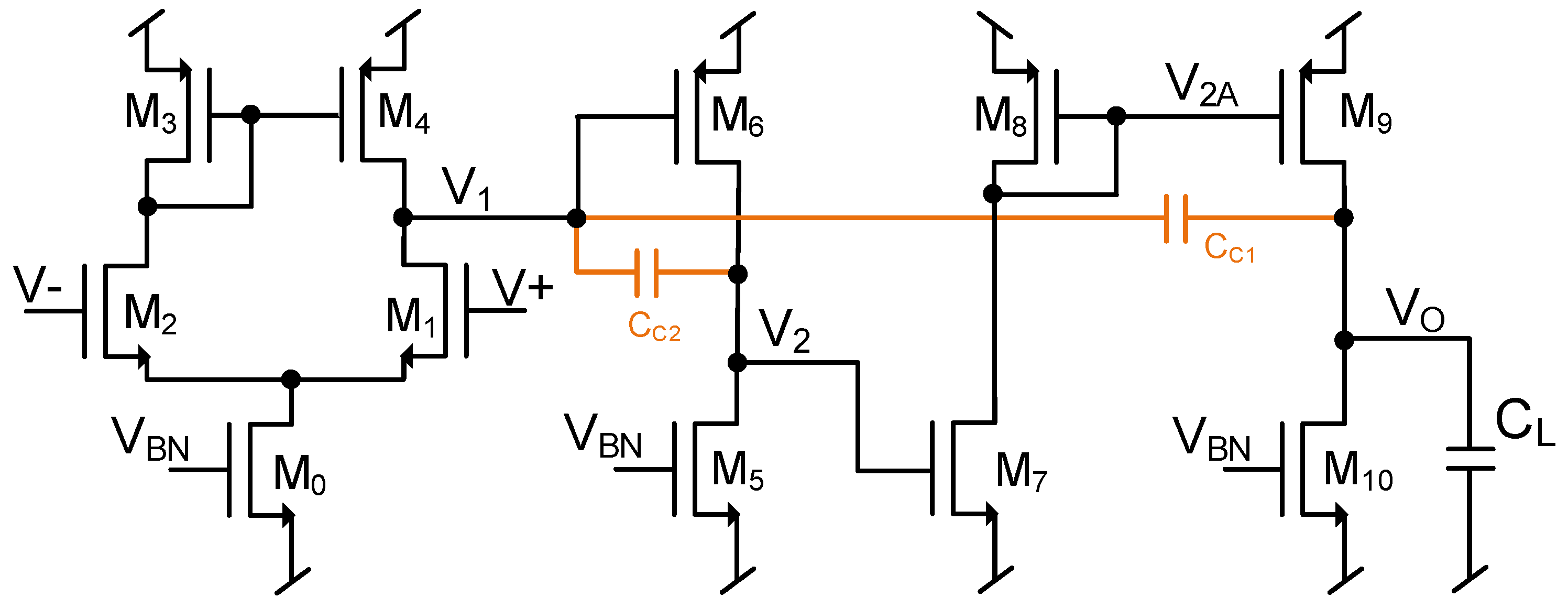
Nested Miller compensation (NMC) is a popular frequency compensation technique used to stabilize three-stage amplifiers [
10], this compensation scheme is shown in
Figure 1. It must be noticed that if
is 0, the circuit shown in
Figure 1 configures to a traditional NMC circuit. The compensation in a NMC scheme uses two capacitors connected between the output node and intermediate nodes of the amplifier. The nulling resistor,
allows cancellation of the RHP zero created by
, and increasing
>
creates an LHP zero which helps in phase boost [
11]. This variant of an NMC circuit is denominated as nested Miller compensation with nulling resistor (NMCNR). The transfer function of NMC with nulling resistor is given by:
where
,
,
,
. Resistors
,
and
are the output impedance at nodes
,
and
, respectively. The transfer function of a traditional NMC can be obtained by evaluating the Equation (
1) with
.
NMC has one RHP zero, one LHP zero and three LHP poles when
. As the compensation capacitors are loading the output, this amplifier suffers from poor slew rate at high frequency. Under the slewing condition,
is required to pull up by charging the load capacitor
, the internal node
is pulled down towards the ground to allow more current to flow through
. When
is pulled low, the compensation capacitor
appears to be in parallel with
loading the output node causing a slow slew rate. Moreover, this changes the overall compensation of the circuit where
disappears and the entire circuit is compensated by
only. This changes the amplifier stability conditions considerably and increases the settling time. To design a stable NMC amplifier, the compensation capacitors must be chosen with the following conditions [
7]:
The load capacitor affects the location of non-dominant poles and gain bandwidth (GBW) product making this compensation suitable only for applications with small range of load capacitance. GBW for NMC is given by [
12]:
Reverse nested Miller compensation (RNMC) is another compensation where the output of the first stage of the amplifier is loaded with both compensation capacitors causing the internal voltage to be slew limited [
13,
14]. Referring to
Figure 2, RNMC requires non-inverting configuration in the third stage between
and
. This limits the driving capability of the output stage due to limited voltage swing on
. The transfer function of RNMC is given by [
13]:
where
, and
.
Multiple advanced compensation techniques are published in the literature to extend the bandwidth, such as the double pole–zero canceling technique [
15], multipath NMC (MNMC) [
10], nested Gm-C compensation (NGCC) [
16] and damping factor control frequency compensation (DFCFC) [
7]. However, all these compensation techniques have strong dependency on output load capacitor for stability. NMC and RNMC with combination of voltage and current buffers are proposed in the literature to isolate the output node or compensate for RHP zero [
17]. The proposed compensation scheme described in the next section solves these challenges.
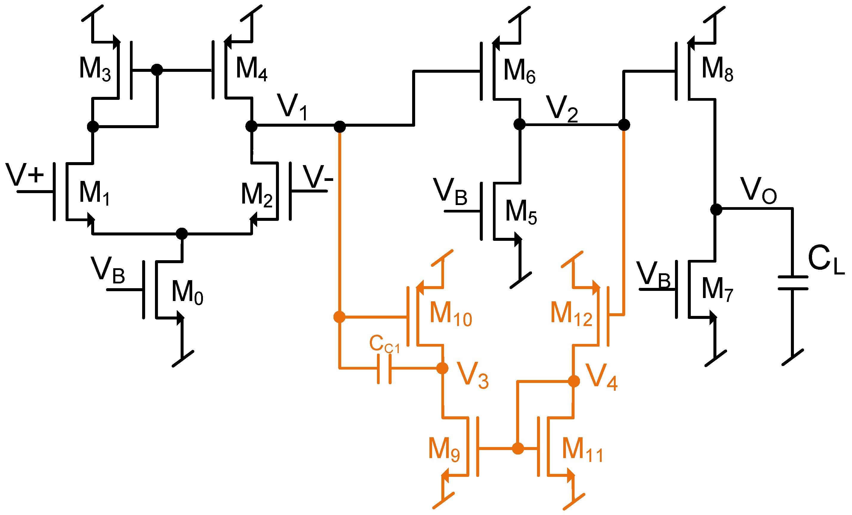
2. Proposed Improved Frequency Compensation
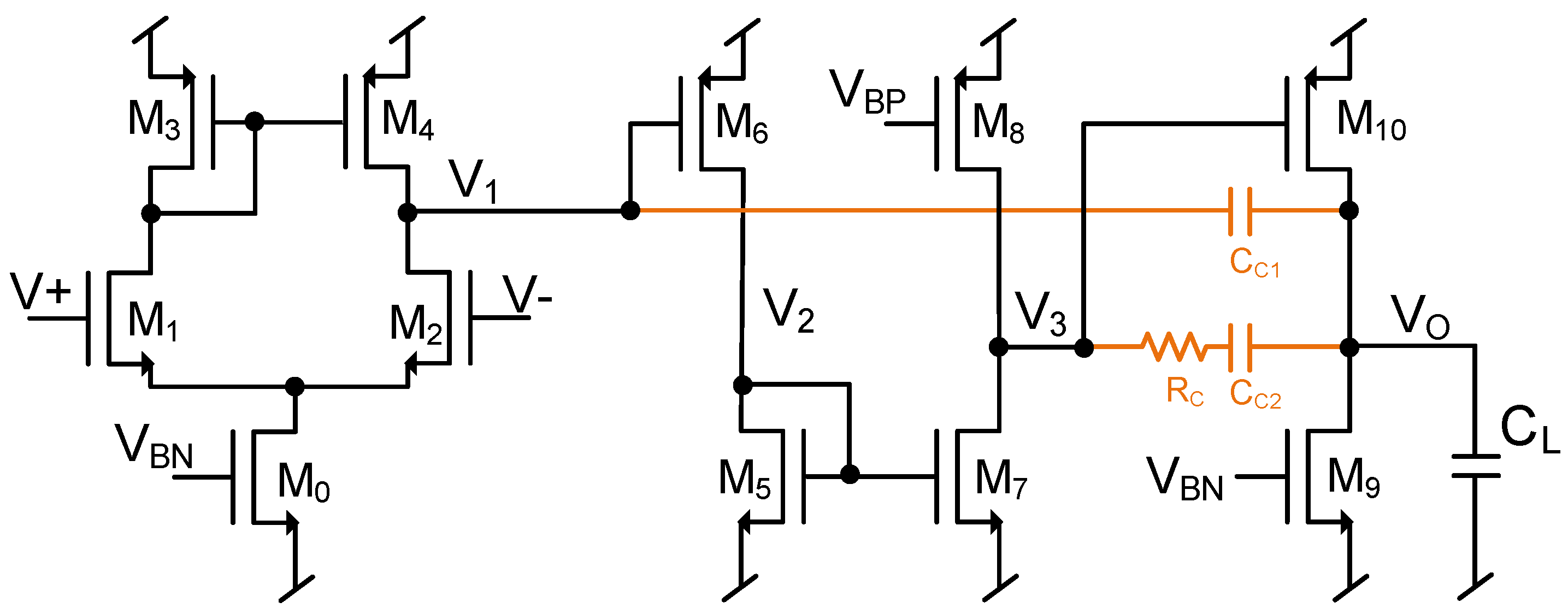
An improved frequency compensation method is proposed using a single capacitor with auxiliary feedback loop connected between the two intermediate nodes as shown in
Figure 3. Typically, the internal nodes of a multi-stage amplifier have a finite voltage swing compared to its output voltage swing. The use of the compensation capacitor on the high-swing output node severely affects the circuit slew rate compared to loading compensation capacitors on internal nodes where the voltage swing is limited. Using this advantage, the proposed compensation scheme uses internal circuit nodes
and
for compensation.
Referring to
Figure 3,
,
and
are the three stages of the amplifier.
are used for compensation, where
and
generate a Miller effect over
adding one LHP zero-pole pair to the amplifier transfer function. The small-signal model for the proposed compensation is shown in
Figure 4, where
,
,
,
and
are the output impedance, and
,
,
,
are the total parasitic capacitances at nodes
,
,
,
and
is the load capacitor at node
. The transfer function is given by:
where
, and
.
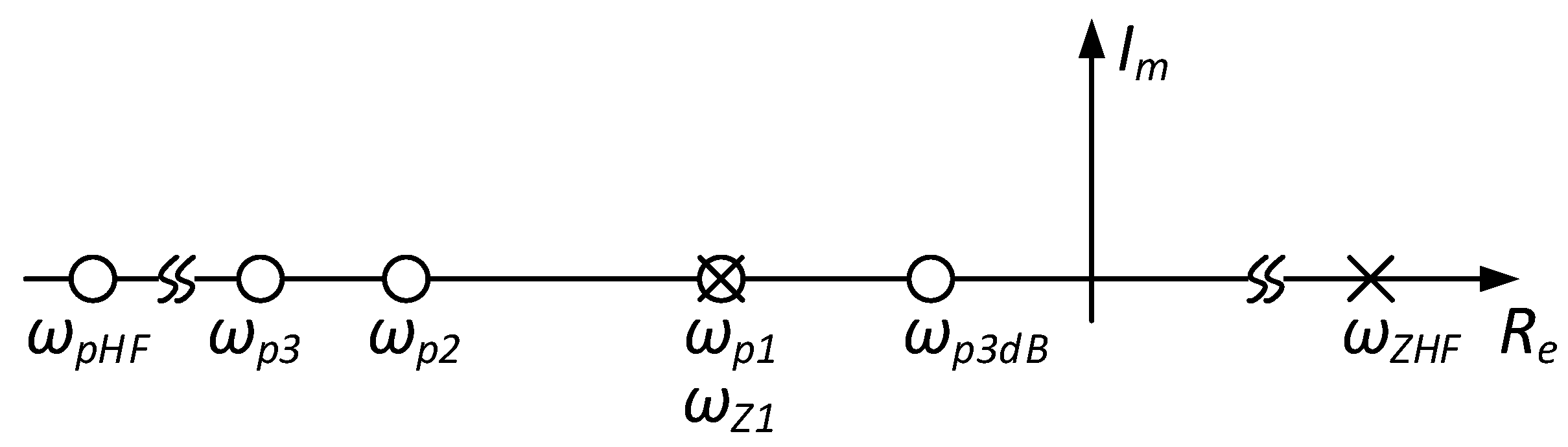
The proposed compensation has one LHP zero and four LHP poles. Two of these poles
are high frequency poles set by
and
parasitic capacitaces at nodes
and
, respectively. Observe that
is connected to a low impedance node and the pole associated with
is located at a very high frequency and can be neglected. Similarly, parasitic capacitance
is connected to a node where the effect of
capacitor is dominant; therefore, it can be also neglected. Additionally, a pole-zero cancellation can be achieved by selecting
≈
, and this condition is controlled by the relationship between the transconductances
and
, where
. The compensation capacitor
can be selected by using
. Observe that the compensation capacitor
can be reduced by increasing the output transconductace
. The dominant pole
at node
is set by
and
, where these gains divide the node frequency pole (
to move the pole to a low frequency. Sizing
adequately, the non-dominant pole (
) can be compensated. If parasitic capacitors are neglected such as most of the models reported in the literature, the transfer of Equation (
6) can be approximated to a single pole transfer function. The pole zero location illustration is shown in
Figure 5, where
and
are a very high frequency pole and zero from intermediate nodes.
Phase margin is given by:
Observe that the pole-zero cancelled transfer function in Equation (
9) yields similar response when well-known techniques such as voltage followers, current followers, and multipath Miller approaches are used [
15]; except that in the proposed compensation, the second and third poles are located at high frequency, which is set by parasitic capacitances at the output of the first and second stages instead of compensation capacitors to provide a phase boost.
Referring to the slew-rate degradation in NMC, the proposed compensation scheme remains connected in the original configuration during slewing condition, and no settling time degradation is observed. The proposed compensation can be used for improved load transient response in LDOs where high output load capacitance is used.
3. Stability Analysis
Phase margin and gain margin are the two essential parameters used to characterize the stability of an amplifier, and they are measured in an open-loop configuration. Nevertheless, these parameters do not guarantee a good stability in closed-loop operation as explained in detail in [
1]. Routh–Hurwitz stability criterion is an alternative method that can be used to identify conditions that make the closed-loop configuration unstable [
18,
19].
For Routh–Hurwitz stability criterion, consider an unitary feedback with a closed-loop gain transfer function given by
in Equation (
10). Observe that the open-loop zero of
in Equation (
6) is part of the characteristic polynomial, and the closed-loop poles positions in the denominator are modified. Therefore, a closed-loop stability should be analyzed using Routh–Hurwitz stability criterion.
The characteristic polynomial of poles in the Equation (
10) can be simplified and represented by:
According to the Routh–Hurwitz stability criterion, it can be concluded that the closed-loop transfer function with fourth-degree polynomial characteristics should meet the following criteria to avoid any RHP pole creation [
1]:
Solving for parameters
,
,
and
from the characteristic polynomial of the transfer function
, the closed-loop stability criterion for the proposed compensation scheme is given by:
4. Simulation Results
A conventional three-stage amplifier with the proposed improved frequency compensation is implemented in a 0.18 μm CMOS process. A conventional three-stage amplifier with NMC, NMCNR and RNMC is also implemented for comparison. All amplifiers are designed to drive a load capacitance of 10 pF with VDD = 1.8 V and DC gain = 90 dB. Transistor parameters are given in
Table 1.
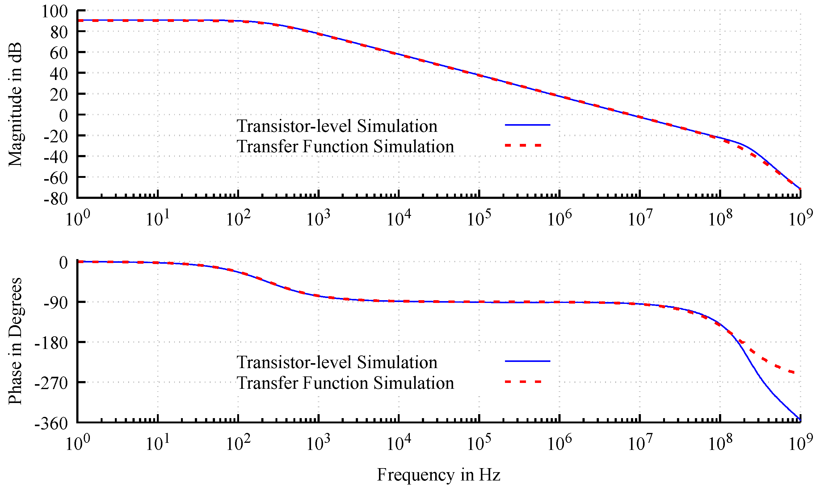
The transfer function shown in Equation (
6) is verified with a simulation of transfer function equation and a transistor level implementation. The ac response of both implementations is shown in
Figure 6. Observe that both AC responses overlap with each other to match up to high frequency. The mismatch at high frequency is due to high-frequency parasitic capacitances that are neglected in the transfer function for simplicity.
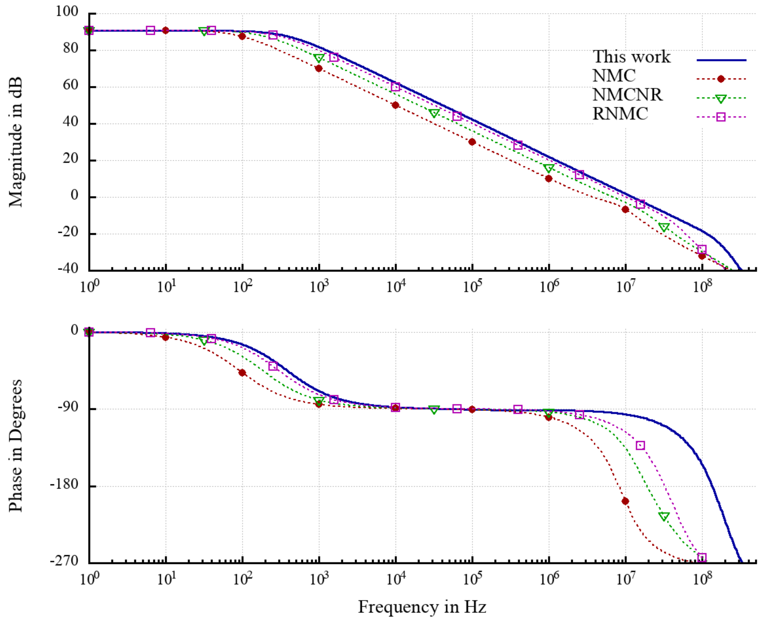
Referring to
Figure 7, the AC response of the proposed compensation scheme is compared with NMC, NMCNR and RNMC compensation schemes. Observe that the response of the proposed scheme almost overlaps with the RNMC scheme, with the difference that the proposed compensation moves high-frequency poles to a much higher frequency. It is clear that the stability of the other compensation scheme is conditioned to maintain a good separation between their high frequency poles set by compensation capacitors, and the high frequency poles set by parasitic capacitances. This limits the highest achievable GBW with relatively good stability, whereas in the proposed compensation scheme, the design can operate with the highest GBW with relatively good stability as no high frequency poles are added. The only limitation is by the increment of parasitic capacitors obtained by growing the output stage transistors. Referring to
Figure 7, the high-frequency improvement achieved by this compensation scheme increased the phase and gain margin showing better stability parameters with respect to the other compensation scheme used to compare the performance of the proposed compensation scheme.
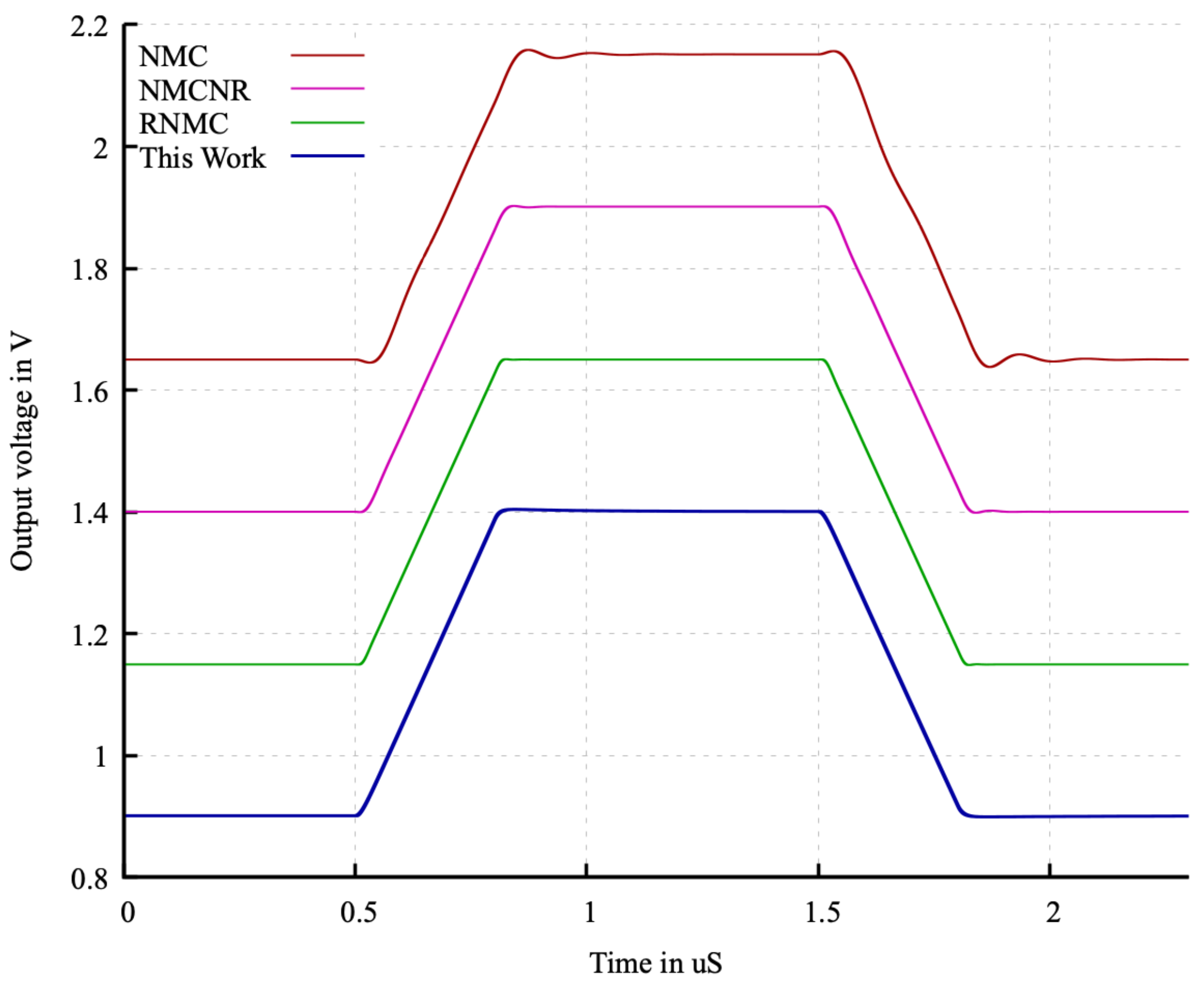
The settling time improvement is validated with large-signal and small-signal step response stimulus at different rise and fall times. For large-signal settling response, a 500 mV pulse with a rise and fall time of 300 ns is applied with a DC offset of 0.9 V to all amplifiers with different compensations, and the response is shown in
Figure 8. Since NMC amplifier has a lower GBW and not good gain margin, some oscillations can be observed in its output signal. NMCNR, RNMC and the proposed compensation showed higher GBW with better phase margin and gain margin, and no oscillations are observed. An intentional large offset is added to the figures for readability.
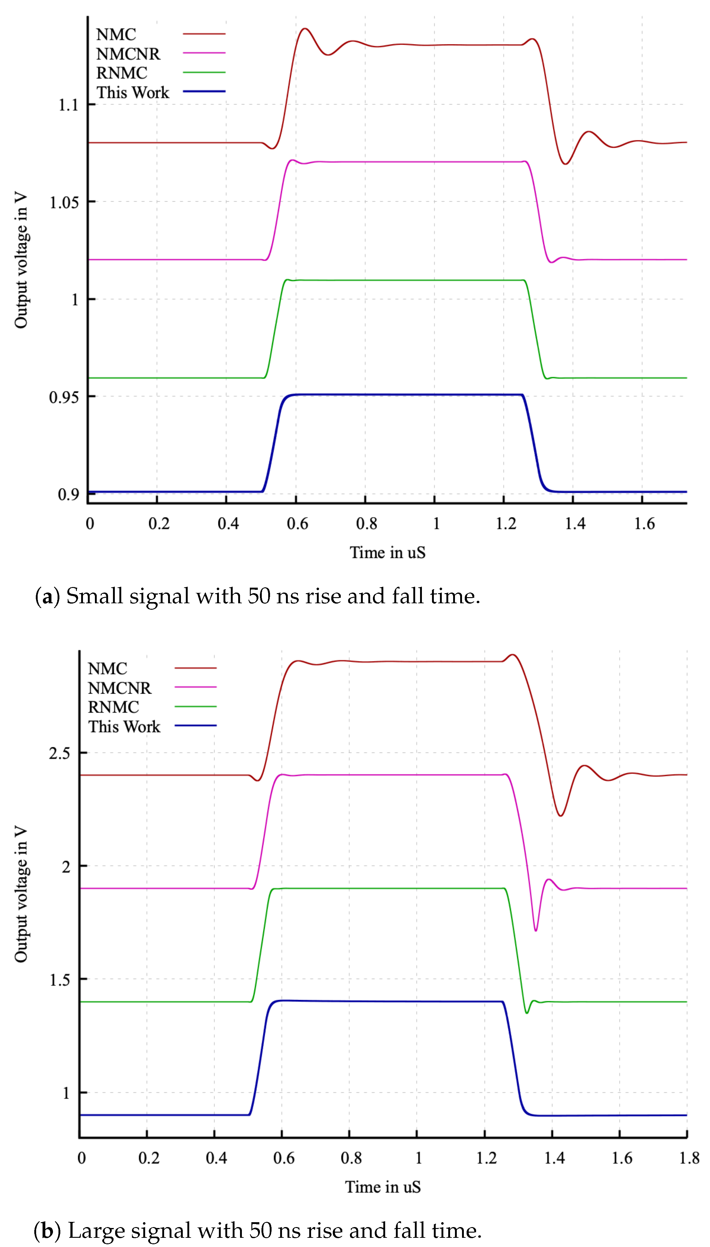
Small-signal settling is validated by applying 50 mV pulse with a rise and fall time of 50 ns as shown in
Figure 9a. Observe that the proposed compensation does not show any voltage ring or peaking due to increased phase margin. Additionally, a large signal settling of 500 mV with a rise and fall time of 50 ns representing the slewing condition is shown in
Figure 9b. Observe that the NMC shows a degraded response and higher fall settling time, whereas the proposed compensation scheme has no degradation during slewing condition. Similar responses are seen in NMCNR and RNMC. RNMC shows reduced fall settling degradation and this can be attributed to the fact that in order to design a stable amplifier, the trasconductance of second stage must be increased, which increases the slew rate and power consumption.
The total compensation capacitance required is reduced from 12 pF with NMC, 5.5 pF with NMCNR, 3.5 pF with RNMC to 2 pF and no nulling resistor. The phase margin is improved from 53 deg to 82.5 deg and the gain margin from 4.71 dB to 21.9 dB when compared with NMC as the proposed compensation scheme do not add high-frequency poles. Moreover, a significant improvement in the slew rate is observed with the proposed compensation. The proposed compensation is compared with the literature and is shown in
Table 2, where unity gain frequency (UGF), DC gain (
), phase margin (PM), gain margin (GM), total compensation capacitance (
), total compensation resistance (
), load capacitance (
), average slew rate (SR), power consumption (P), and figure of merits (FOM) are given. Observe that the proposed scheme slew rate is 146% higher than NMC and 60% higher than NMCNR. RNMC has similar slew rate but consumes high power. Three different figures of merit (FOMs) are used to compare the performance of the proposed compensation scheme and are shown below. A FOM proposed in [
14],
considers GBW, total sum of all transconductances and compensation capacitances. Observe that the proposed compensation scheme has higher
,
,
,
, and
. A summary of stability and settling time results is the proposed compensation are shown in
Table 3.
The process corner simulation results at different temperatures are shown in
Table 4. Observe that the phase margin and gain margin are maintained greater than
and 22 dB, respectively. A maximum deviation of 3.9 MHz is observed for unity-gain frequency from typical process and room temperature. Despite the process variation, the proposed compensation scheme maintained good stability for a temperature range from
to
.


 ,
, 


