Article

An Experimental Study on Step-Up DC–DC Converters for Organic Photovoltaic Cells

by
P. Mendonça dos Santos
1,2,*,
António J. Serralheiro
1,3,
Beatriz Borges
2,
João Paulo N. Torres
1,2 and
Ana Charas
2
1
Academia Militar (AM), CINAMIL, Instituto Universitário Militar (IUM), DCEE, Campus da Amadora, 2720-113 Amadora, Portugal
2
Instituto de Telecomunicações, Av. Rovisco Pais 1, 1049-001 Lisboa, Portugal
3
INESC-ID, 1000-029 Lisboa, Portugal
*
Author to whom correspondence should be addressed.
J. Low Power Electron. Appl. 2022, 12(2), 20; https://0-doi-org.brum.beds.ac.uk/10.3390/jlpea12020020
Submission received: 11 March 2022 / Revised: 1 April 2022 / Accepted: 5 April 2022 / Published: 8 April 2022
(This article belongs to the Special Issue Energy-Harvesting and Self-Powered Devices)

Abstract

:
This work studies two circuit topologies to step-up the voltage supplied by an organic photovoltaic (OPV) cell. Comparison and validation of the proposed topologies are accomplished throughout analytical, simulation, and experimental results. Two circuit solutions were found more suitable to boost the harvested OPV cell low voltage, depending on the load condition: the classical hard-switching boost converter and a multilevel boost converter. Both experimental circuits include the drive of the MOSFET switch based on an LC oscillator at 1.2 MHz, allowing the implementation of a conversion system, supplied by voltages as low as 500 mV, with output voltages from 1.2 V up to 7 V, under solar simulator conditions. The circuit area for each converter prototype is 2.35 cm 2 , with a total area below 3.0 cm 2 for the overall energy harvesting system, including the OPV cell, which makes this proposal an extremely compact solution for ultra-low power harvesting applications.

1. Introduction

Advancements in the field of remote and mobile sensing, namely with the arrival of Internet-of-Things (IoT) applications, which calls for wireless sensor networks, or biomedical monitoring based on wearable sensors, implies that some of these applications have a long lifetime, and the use of conventional batteries is not always advantageous, since it requires periodical human intervention. In this way, using forms of obtaining electric energy from the environment—energy harvesting—is becoming more and more under investigation, allowing the supply of almost unlimited energy for the useful life of a specific group of electronic devices [1].
The use of switch mode step-up DC–DC converters is a solution to increase the normally low voltage values of these energy harvesting sources, either based on inductor topologies or inductorless switched-capacitor topologies [2]. However, designing these switch-mode DC–DC converters for such low-power (<10 mW) and low-voltage (<1 V) applications, such as the voltage and power levels obtained from the most common ultra-low power (<1 mW) energy harvesters (solar, RF, piezoelectric, etc.), is very challenging. Several research works have been reported that allow to convert the energy received from the harvester to an adequate DC level to supply IoT, remote, or portable and wearable circuitry. For example, a discrete half wave rectifier is proposed in [3] to convert the RF AC voltage from wireless electromagnetic waves to an unregulated DC voltage. In [4], another discrete full-wave voltage rectifier is used to convert the AC voltage from a piezoelectric mechanical vibrator to a DC voltage bellow 6.5 V (470 μW) and, in [5], a similar work based on a hybrid solution is proposed. This circuit comprises a CMOS rectifier and discrete filtering components on a PCB. The authors achieved an output voltage of 700 mV for a 45 k Ω load (≈110 μ W).
In [6], a discrete AC–DC voltage doubler is cascaded with an inductive boost converter to provide voltages above 2.5 V (500 μ W). Other works (e.g., [7]) report RF AC–DC conversion based on inductor-less switch-capacitor topologies. Another example of RF AC–DC conversion is reported in [8]. The paper describes a discrete prototype of a resonant DC–DC converter topology supplied by a planar antenna. The circuit increases the ultra-low input voltage (>100 mV) to usable levels for an ultra-low power output of a few μ W.
Other authors use well-known power electronics topologies to adapt the conversion to ultra-low power applications. The work reported in [9] presents an interesting approach to this ultra-low power, with an energy harvesting source based on a microbial fuel cell. The PCB prototyped converter is a buck-boost capable of delivering an experimental output voltage above 2.7 V for a 510 k Ω load (14 μ W output).
Other approaches resort to CMOS technology to design hybrid solutions with off-chip reactive elements to convert the DC low voltage from other energy harvesters. In [10], the system is designed to step-up the low voltage from a thermoelectric generator, resorting to a two-stage auxiliary boost and a voltage multiplier with large duty-cycle, to achieve a regulated 1.25 V output voltage for a maximum power of 540 μ W. The authors in [11] also propose a flyback DC–DC converter solution to increase the voltage from a thermoelectric generator to obtain an output voltage of 5 V. Likewise the previous two works, in [12] it is reported a CMOS based solution to step-up the voltages from energy harvesting sources, this approach being based on a boost DC–DC converter topology with a maximum output voltage of 1.8 V.
Another work related to ultra-low power is presented in [13], where the authors design a self-resonating boost converter to achieve a maximum of 3 V from input voltages in the range of hundreds of mV.
In [14], a boost converter solution with an extra inductor in recycled is compared to synchro-recycled techniques, by exploiting the non-linearity of the photovoltaic (PV) cell, to achieve output voltages below 2.7 V for an output power of tens of mW.
Other works report DC–DC converter topologies targeted to medium to high power conversion, especially for PV energy harvesting [15,16,17]. However, for ultra-low power applications, with a few mW and a few hundreds of mV available from the energy harvesting source, the majority of the circuit solutions, based on a high complexity and component count, are not viable. In fact, restrictions in the voltage available to control semiconductors to on-state and, at the same time, component on-state losses, will compromise the converter voltage multiplication factor.
The goal of this proposed work is the performance evaluation of two inductive step-up DC–DC converter topologies in surface-mount technology (SMT), to increase the voltage supplied by an organic photovoltaic (OPV) cell, to a voltage above standard values (1.2 V, 2.4 V, etc.), depending on the load resistance value. The resultant OPV cell with the converter system, that may emulate a battery, can be used to directly supply biosensors, IoT remote nodes, and other ultra-low power portable circuits, to accomplish self sustainable and powered electronic systems.
The paper is divided in six sections. Section 2 presents the fabricated OPV cell and correspondent circuit model used in simulations. Section 3 focuses on the converters under study: the well-known boost hard-switching converter and a boost-based multilevel converter adapted from the work reported by other authors in [18]. Analytical results are shown and compared with simulations. Section 3 also includes the challenges, trade-offs and design criteria of both systems, including the design details of an LC MOSFET driving oscillator. In relation to Section 4, results of the experimental implementation are shown with both converter prototypes tested under solar simulation condition and also powered by a voltage source. Finally, the conclusions are presented in Section 5.

2. The Organic Photovoltaic Cell

The OPV cells were prepared on ITO (100 nm thick)-coated glass substrates. The ITO surface was submitted to UV-oxygen plasma for 3 min and PEDOT:PSS was spin coated from as an aqueous dispersion (Clevios PVP AI4083, from Heraeus) on top to yield a ca. 40 nm thick layer. The glass/ITO/PEDOT:PSS substrates were then dried at 125 C for 10 min. The organic/active layer was prepared by dissolving the polymer F8T2 (polydioctylfluorene-alt-bithiophene) (ADS) and the fullerene PC60BM (Solene BV) in a 1:2 mass ratio in chlorobenzene (total concentration = 30 mg/mL), under stirring, for 3 h at 75 C. The solution was then spin coated over glass/ITO/PEDOT:PSS substrates to yield a film with ca. 100 nm thick. Following the deposition of the active layer, LiF (1.5 nm) and Al (100 nm) were thermally evaporated on top, through a shadow mask, under a base pressure of 2 ×   10 6 mbar, defining a device area of 0.24 cm 2 . Two contacts of LiF/Al were deposited per each device substrate. Figure 1 shows a cross section view of the fabricated OPV cell.
The cells were protected from air contamination and moisture by encapsulating the devices with glass plates and a transparent light-curable epoxy-type sealant. Figure 2a shows an example of the fabricated substrates in which two pixels, P1 and P2, have been implemented, each corresponding to a different OPV cell, with an individual active area of 0.24 cm 2 . Each substrate contains two upper aluminium contacts and one lower tin contact, the lower electrode being common to both pixels. Table 1 summarises the average performance parameters calculated from a set of 8 substrates, containing 16 OPV cells J-V curves, under illumination (85 mW/cm 2 ). Figure 1b shows a J-V curve taken as representative for the cells performance. The OPV were electrically modelled to be included in simulations with EDA tools. The model is based on the classical circuit represented in Figure 2b, where the current generator represents the overall I s c current obtained by paralleling both P1 and P2.

3. Step-Up Voltage Inductive DC–DC Converters

3.1. Problem Statement

This section includes the description, theoretical analysis, and preliminary evaluation of the two topologies under study: the classical hard-switching inductive boost converter and the multilevel boost converter, based on the adaptation of the work reported by other authors in [8]. The challenge in this work is the low power delivered by the OPV cell and, particularly, its low output voltage, which is below standard MOSFET threshold voltages. Furthermore, for this ultra-low voltage applications, semiconductor devices on-state voltage is of the same order of magnitude of the supply voltage, and can become the bottleneck of the voltage step-up process. On the other hand, these electronic systems are usually designed on recent CMOS technology nodes (tens of nm), which consumes a very low current with supply voltages as low as 1.2 V. For such low-power light-load (tens or hundreds of k Ω ) applications, the converter semiconductors must be chosen accordingly, with near zero threshold and very low on-state voltages. As will be explained, this can become a challenging task for discrete circuits, based on components off-the-shelf (COTS).

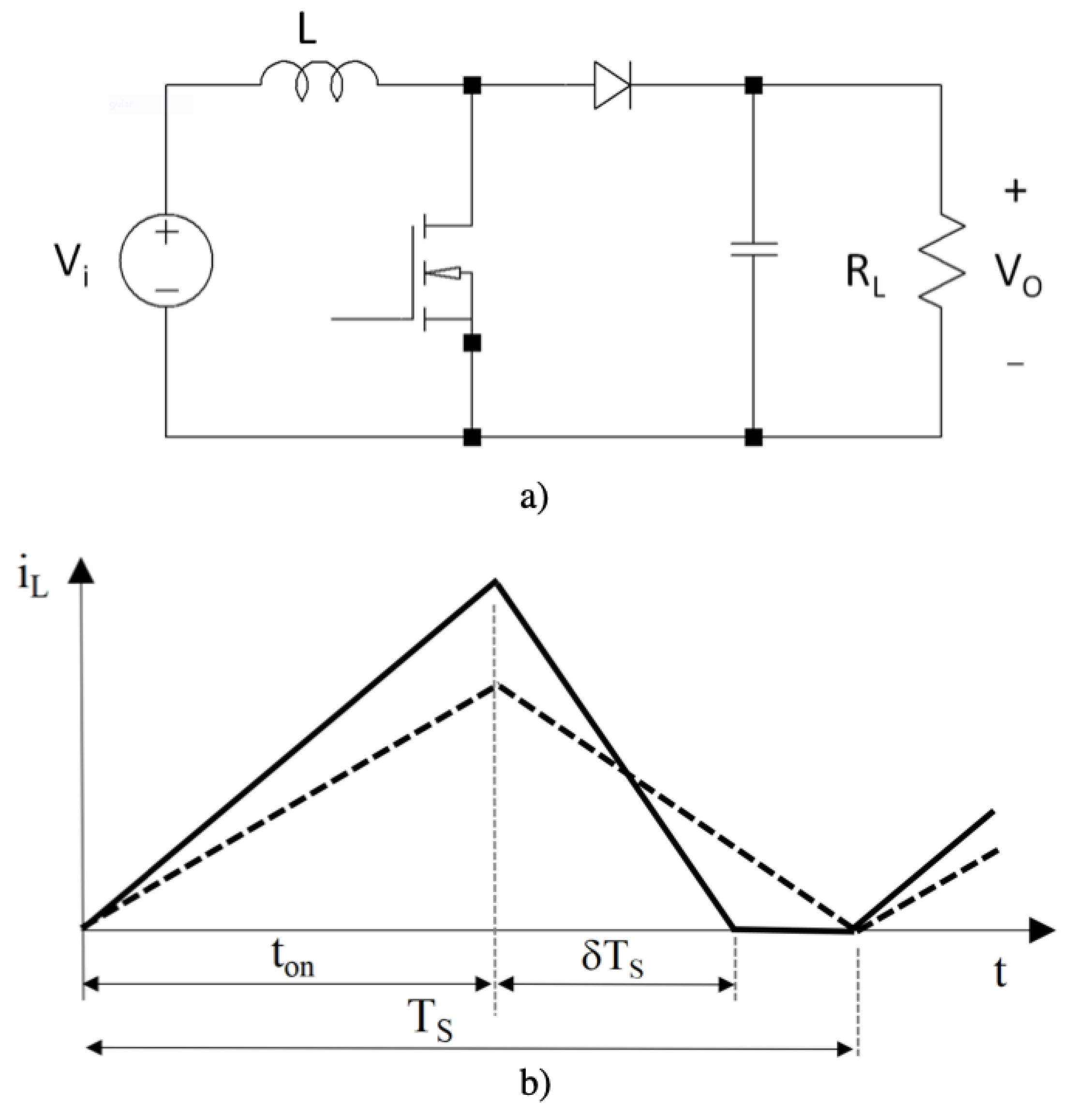
3.2. The Hard Switching Boost Converter

Figure 3 shows the classic hard-switching inductive boost converter. The ideal control of the MOSFET switch is based on a square-wave signal, with frequency f s and duty-cycle D = t o n / T s . For the ideal converter the semiconductors can be firstly considered as ideal switches. In this case, the converter output voltage is only dependent on the input voltage ( V i ), and duty-cycle D, so
V o = V i 1 D
and I o = ( 1 D ) I i ), as long as the converter remains in the continuous-conduction mode (CCM), i.e., if the inductor current remains positive all along the switching period, T s . For a fixed input voltage, switching frequency, and duty-cycle, the inductor peak and average currents are dependent on the inductor value, since Δ I L is a function of 1 / L . As can be seen in Figure 3b, the limit of CCM corresponds to the inductor current represented by the dashed line.
The limit value for the inductor at CCM, L lim , can be derived from the analysis of the circuit at the MOSFET on-state.
At the limit of CCM, represented by the dashed line in Figure 3b, the converter output voltage can be derived from the average inductor current as,
V o = 2 L f s I L ¯ D ( 1 D )
where I L ¯ , the average inductor current, is also the converter input current, I i . Taking into account that v L = V i during t on , and considering a lossless circuit, Equation (2) can be rewritten as
V o = 2 L f s I o D ( 1 D ) 2
Rearranging the above equation for a resistive load R L , with a continuous-current I o , Equation (4) defines the inductor value for the limit of CCM
L lim = D ( 1 D ) 2 R L 2 f s
For L < L lim , the converter enters in DCM, as represented by the inductor current waveform in Figure 3b (solid-line). The output voltage in DCM can be derived from the inductor voltage over a period,
V i D T s L + ( V i V o ) δ T s L = 0
to calculate δ
δ = V i D V o V i
The average current in δ T s is the average output current, since the MOSFET is at off-state
I o = I L max δ 2 = V i 2 D 2 f s L ( V o V i )
where I L max is the inductor peak current calculated at the MOSFET on-state. For a resistive load, R L , V o can be computed as a function of the circuit specifications and design variables
V o = V i 2 + V i 2 1 + 2 D 2 R L f s L
The above design Equations (4) and (8) can be simplified for the case D = 0.5 (voltage doubler in CCM)
L lim = R L 16 f s
V o = V i 2 + V i 2 1 + R L 2 f s L
The analysis of Equation (10) clearly shows that the step-up magnitude can be increased above the CCM voltage doubler ( V o = 2 V i , for D = 0.5 ) with the appropriate inductor and switching frequency, for load values above R L > 16 f s L , as long as the inductor value is also below L lim . This DCM solution can be promising when the goal is circuit miniaturization for ultra-low power applications, such as in this proposal, circuits powered by an OPV energy harvesting source. Further reduction in magnetics’ and capacitors’ volumes can be achieved if the converter is designed with an increased switching frequency.

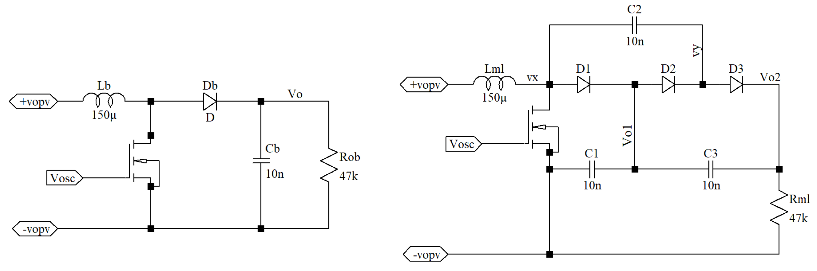
3.3. Multi-Level Boost Converter

A multilevel boost converter, usually tailored for high-power and high-voltage applications, was also under investigation to further increase the low OPV output voltage. Although miniaturization and complexity reduction objectives are paramount for the proposed step-up DC–DC conversion system, a two level ( N = 2 ) converter was chosen in order to compare its performance with the classical hard switching boost converter, for this specific low-voltage application. The circuit is represented in Figure 4.
As can be seen, the input stage of this topology is identical to the boost converter. Let us consider that the MOSFET switch is controlled by an identical square wave, with equal switching frequency f s and duty-cycle D. After the circuit transient response, the voltage value at node vo1 is similar to the boost hard switching topology case. When the MOSFET switch is off the inductor current increases linearly, diodes D1 and D3 are off, and capacitor C2 is charged through D2 with vo1. When the MOSFET is turned off, D1 and D3 are turned on, D2 is turned off, and capacitor C3 is charged through D3. The voltage at the load is then the sum of the voltages at C1 and C3, since vc1 = vo1 and vc2 = vo1. Therefore, the N = 2 multilevel stage is a voltage doubler, and its output voltage at CCM is
V o ml = N V i 1 D = 2 V i 1 D
which corresponds to four times the input voltage if D = 0.5 . In this case, the output current can also be related to the inductor and input converter current, I i = 2 I o / ( 1 D ) . Again, assuming a lossless analyses ( P o = P i ), it can be concluded that the critical load to enter DCM is
R L lim = 8 L f s ( 1 D ) 2 D
which becomes R lim = 64 L f s for D = 0.5 , i.e., the load limit to enter DCM is four times higher than the case of the hard switching boost topology. This indicates that the multilevel solution can become interesting when the objective is to achieve higher voltages at high resistive loads. The N = 2 multilevel converter output voltage at DCM can be computed with the aid of the classical boost Equation (8), with V o 1 = V o 2 / 2 and considering the load resistance R L ml of the multilevel converter equal to four times the R L of the boost converter
V o = V i + V i 1 + D 2 R L ml 2 f s L
and, for D = 0.5
V o = V i + V i 1 + R L ml 8 f s L
Figure 5 shows, respectively, the output voltage for the classical boost and the multilevel converter, as a function of the resistive load value (from 1 k to 100 k Ω ), for a set of input voltages (from top to bottom, 1000 and 600 mV), assuming a symmetric ( D = 0.5 ) switching signal of 1.2 MHz and for an inductor L = 150 μ H. The flat behavior at low resistive levels were computed according to the converters operation at CCM mode, as by Equations (1) and (11), while the complementary curves were obtained with Equations (10) and (14).
As can be seen, the multilevel converter output voltage is always above the output voltage of the boost topology for the same input voltage, but this difference is more relevant for high-output currents (lower load values), with the converters operating in CCM. On the other hand, both topologies evidence high-voltage conversion ratios (Vo/Vi) for light loads (high resistance).

3.4. Design Challenges for the Proposed Solutions

This subsection discusses the low power and low voltage circuit design challenges and correspondent solutions. Semiconductor losses are addressed, in order to understand the problem associated to driving a transistor gate with voltages slightly above standard threshold levels, while maintaining on-state losses low enough to attain a relevant conversion ratio. An oscillator to drive both converters MOSFET is proposed according to the voltage and power design constraints. The evaluation of the two proposed systems is then performed with the aid of circuit simulation, in order to obtain design strategies for experimental prototyping.

3.4.1. Semiconductor Devices

Low voltage DC–DC converter circuits presents challenging design problems, especially due to the constraints in power supply for auxiliary subcircuits, such as MOSFET driving oscillators, but also because semiconductor on-state voltage losses can be dramatically relevant. In fact, for an input voltage in the range of hundreds of mV, the on-state voltage of a regular silicon diode is not admissible. For the system under investigation supplied with the OPV cell, the converter input voltage is below 1 V, with nominal input voltages above 500 mV, and currents that can be as low as tens of μ A. At this voltage and current levels, the converter diodes must be Schottky in order to keep on-state losses below a very few hundreds of mV. Furthermore, driving a classical MOSFET into triode with a nominal threshold voltage of the same magnitude of the input voltage is not possible. It is crucial to select a near-zero threshold voltage MOSFET, since the OPV output voltage (which is the converter input voltage) can now be used to drive the device to a reasonably low on-resistance value. On the other hand, the design of an oscillator to drive the converter switch, supplied by the OPV, is also a challenge, since the semiconductors at the amplifier circuit must be in saturation with reasonable current values enabling them to keep the oscillation.

3.4.2. MOSFET Driving Oscillator

As mentioned, the objective is to design an energetically autonomous DC–DC converter, powered by the low output voltage OPV cell. For the proposed classical and multilevel boost topologies this design includes a MOSFET driving signal, with constant frequency and duty-cycle. Figure 6 shows the proposed LC Colpitts oscillator, involving a common source amplifier with a tuned LC positive feedback loop. Here, the challenge is to meet the oscillation criteria for such a low-voltage supply and MOSFET threshold voltage. In fact, to surpass the losses in the passive LC positive feedback and to maintain an oscillation at the output, the MOSFET biasing is critical.
Taking this into account, the oscillator semiconductor device is also chosen to be a zero threshold voltage MOSFET. This can be an advantage, since both the converter switch and the amplifier semiconductor can be included in the same package, to reduce the system footprint area. The oscillating frequency for the proposed circuit is well-known, depending only on the LC feedback topology
f osc = 1 2 π L C 1 C 2 C 1 + C 2
For this common-source topology, and for the proposed operating conditions, the parasitic capacitances of the MOSFET can also contribute to a variation in the ideal oscillating frequency value obtained with Equation (15). In fact, gate-source and drain-bulk capacitances are added to C 1 and C 2 , respectively, leading to a slight increase in f osc . However, the positive feedback of gate-drain parasitic capacitance, C gd , influences more significantly the real oscillation frequency value. Accordingly, the transfer function for the tuning network, with the inclusion of parasitic capacitance cgd, can be calculated to be
f osc = 1 2 π L ( C gd C 1 + ( C 1 + C gd ) C 2
Considering the resonant feedback circuit it is straightforward to derive its transfer function
H ( s ) = g m · R D ( 1 + s 2 L C g d ) s 3 R D L ( C 1 C g d + C 1 C 2 + C 2 C g d ) + s 2 L ( C 1 + C 2 ) + s R D ( C 1 + C 2 ) + 1
whose frequency response is depicted in Figure 7a. Figure 7b shows the root-locus diagram of the feedback circuit transfer function, where it can be seen the path of the open-loop poles as a function of the MOSFET’s transconductance g m towards its zeros and ; the imaginary axis being crossed at the oscillation’s frequency for the critical g m .
From the Bode diagrams it can be easily seen that the oscillating frequency occurs at 1.2 MHz since, at this frequency, an exact 180° phase lag and the corresponding gain is appropriate to start the oscillator.

3.5. System Evaluation and Design Assessment

Taking into account the specificity of the energy harvesting system, based on a low-voltage OPV cell, both topologies were under study with the aid of circuit simulation, to obtain application specific solutions. The criterion for system design was the selection of reactive and semiconductor elements to obtain an optimized DCM operation for both converters, since this mode is prone to a more significant increase in the converters output voltage. For comparison purposes, the converters were evaluated for the same inductor value (150 μ H), filtering output and multilevel capacitors (10 nF), and ideal on-state semiconductors.
The simulated circuits for the classical boost and multilevel converters are depicted in Figure 8 left and right, respectively.
Preliminary simulations with both converters and oscillator supplied by the OPV cell electrical model were performed, to evaluate converters power-up and steady-state performance, especially in DCM. The simulated waveforms for the inductor current, MOSFET driving voltage and converter output voltage are shown in Figure 9, for the converters under study, with the MOSFET switches driven by the same LC oscillator output voltage (Figure 6), and considering a short-circuit OPV current I s c = 2 mA, which corresponds to two cells in parallel (Figure 2a), and a load value of 47 k Ω . As can be confirmed by the inductor current waveforms, both converters operate at DCM for this load resistance.
Further simulations were performed in order to evaluate both topologies performance and deviations from the theoretical study. Figure 10 shows the result of the assessment of semiconductor losses in the two systems. In this case, the OPV cell was replaced by an ideal voltage source of 0.65 V, which individually supplies the converter and the LC oscillator. The different curves indicate the circuit response to the imposed semiconductor on-state losses, considering first the ideal case, with zero diode forward voltage and the MOSFET with a high transconductance parameter to keep on-resistance at lower limit values. In these conditions, the converters output the maximum voltage, with the multilevel converter output voltage above the classical boost for the overall load resistive range under study. Imposing a forward voltage drop in the converters diodes ( V F = 0.1 V and V F = 0.2 V) results in a decrease in the output voltage. However, this decrease is obviously more relevant for the multilevel converter, since current flows through more than one diode in a gate control period. Of course, the effect of non-zero forward voltage is also more relevant for the heavy load range. Imposing a lower value for the MOSFET transconductance parameter, together with a diode voltage drop of 100 mV is depicted in both purple curves in Figure 10. With this correspondent higher on-resistance, both converters inductance current peak values are reduced. In this way, the output voltage is degraded, with a severe reduction for the multilevel converter at low resistive loads. These preliminary simulation results indicate that the higher theoretical conversion ratio of the multilevel topology is prone to be restrained to the range of light loads.

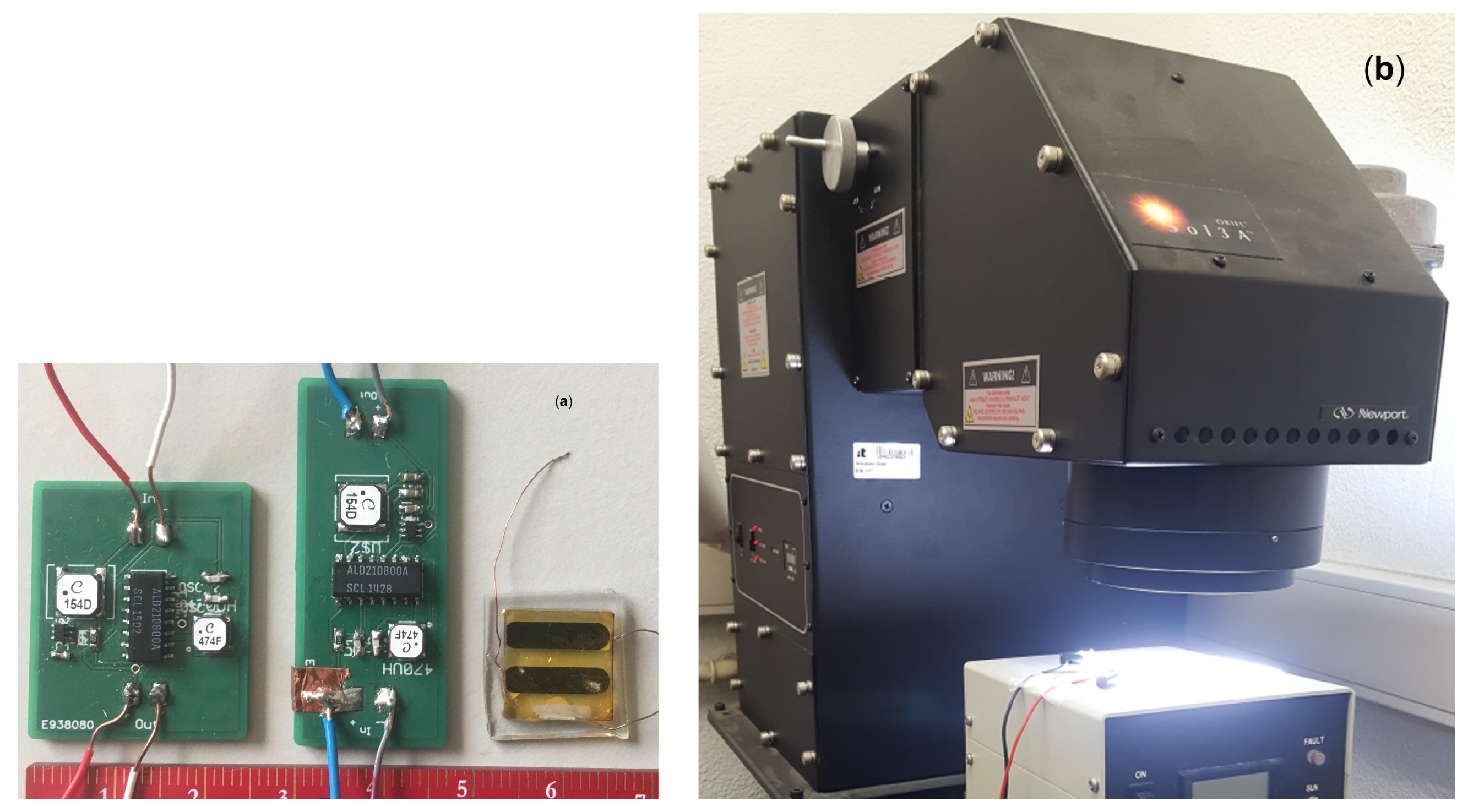
4. Prototypes and Experimental Results

The experimental validation of the designed systems was carried out based on the prototyping of both converters under study. The prototypes were fabricated with low profile SMD components off-the-shelf (COTS) and optimized for a low footprint PCB layout. The circuits for the boost and multilevel converters, including the LC MOSFET driver are shown in the photographs of Figure 11, together with the OPV cells in the glass substrate. Both converters were designed with identical reactive elements ( L = 150 μ H and C = 10 nF) and semiconductors (RB731XN Schottky diodes and ALD210800 MOSFET). The oscillator is identical for both prototypes, and is based in the circuit of Figure 6 ( C 1 = 10 pF, C 2 = 47 pF, and L = 470 μ H). The prototype active areas were similar and measured with 2.35 cm 2 .

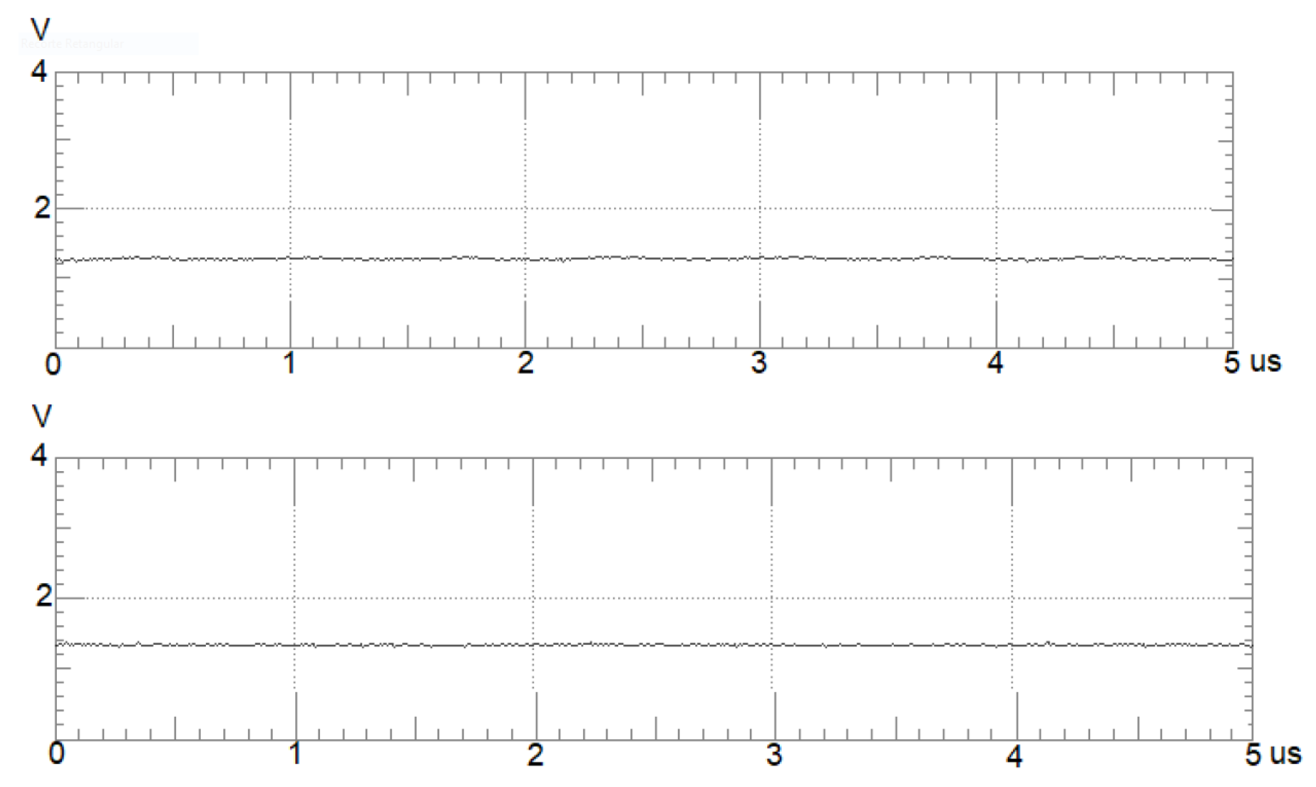
4.1. Systems Supplied by a Voltage Source

Both systems were, firstly, tested considering a range of input voltages (600, 800, and 1000 mV) obtained from a software controlled voltage source, for a set of resistive loads (1, 2.2, 5.1, 10, 47, and 100 k Ω ). The graphics of Figure 12 show the experimental output voltage of the converters obtained with both systems powered by the referred voltage supply.
The observed general trend of an increasing output voltage with an increasing value of the load resistance depicted in Figure 12 is, of course, expected, following the model (for the light load range) and simulation losses predictions (for the heavy load range).
The mismatch between the theoretical and simulation results at heavy loads is confirmed with the experimental results. In fact, for this lower resistive values the classical boost converter output voltage surpasses the multilevel solution, mainly due to the more relevant MOSFET and diode losses.

4.2. Systems Supplied by the OPV

To perform the tests of the circuits with the OPV as a power supply, a solar simulator with AM1.5G illumination (Oriel Sol 3A, 69920, Newport) was used, which can be observed in Figure 11b.
The time diagrams of the output voltage of the two conversion systems can be seen in Figure 13. These diagrams were obtained with a measured supply input voltage of 0.63 V obtained by the OPV under solar simulator radiation, with a load of 10 k Ω at the output. As can be seen, at these conditions, both converters attain a similar output voltage slightly above 1.2 V. Increased converter output voltages can be obtained for higher resistive values.
Table 2 presents both converters experimental output voltage from the OPV cell ( V i n ) illuminated by the solar simulator (Figure 11) feeding the converters for different resistive loads. As can be seen, the output voltage levels are similar for load values around 10 k Ω . For light loads, when the converter power is at its minimum, the multilevel converter output voltage is always above the classical boost converter topology. It should be noted that, for an output with no resistive load, i.e., for the converters loading the capacitive output filter, the output reaches voltages above 4 V and 7 V, for the classical boost and the multilevel converter, which corresponds to conversion ratios above 6.4 and 11.3, respectively.

5. Conclusions

This work presents the experimental performance of two prototyped step-up DC–DC converters targeted to increase the voltage harvested from an OPV cell. Both systems were based on fully discrete COTS on a PCB substrate, resorting to low profile SMD devices, in order to achieve a compact solution. The prototypes include the DC–DC conversion circuit, either based on a classical boost or a multilevel converter, and the MOSFET driving circuit, based on a 1.2 MHz LC oscillator. It is important to emphasize the low number of components for the proposed solutions (8 and 10, respectively, for boost and multilevel converters), achieving a low footprint PCB area of the same magnitude of the OPV cells.
The converters allow a minimum output voltage above 1.2 V for the circuits powered by the OPV cell under a standard solar radiation condition, for resistive loads above 10 k Ω . Maximum voltages above 2 V and 3 V can be attained for lighter resistive loads at the same solar radiation condition.
Both the converters and the oscillator operate at very-low supply voltages in the order of hundreds of mV. It is important to note that the design and operation in DCM grants a high conversion ratio for both topologies, especially in the case of light loads.
From the converters performance point of view, it is important to refer the viability of both topologies to the voltage step-up process, with input voltages above 500 mV and load resistive values above 1 k Ω . However, from the evaluation of simulation and experimental results it becomes clear the adequacy of each converter according to the load and input voltage specification. In fact, in opposition to the theoretical analysis, there is a boundary where the boost converter conversion ratio is above the classical boost converter ratio. This was clearly attributed to the excess losses in the semiconductors for the heavy load (low resistance/high current) condition. As can be seen in Figure 12, this advantage is reduced when the input voltage increases. For the case of the systems supplied by the OPV, the input voltage is slightly below 700 mV, and the boundary of a 10 k Ω load (refer to Table 2) can be specified as the maximum value to consider advantageous the classical boost topology.
For increasing input voltages and load values, the multilevel converter presents a conversion ratio always higher than the classical boost converter. This can be the case of a solution with OPV cells in a serial connection, or other energy harvesting sources, such as piezoelectric or thermogenerators. The multilevel converter is also an interesting solution for capacitive loads, as long as its value is of the order of magnitude of the converter output filtering elements (tens of nF), since the limited converter output current is a serious constraint to charge the low capacitor ESR in these ultra-low power applications.
The proposed system, composed by an OPV cell supplying the converter system may emulate a battery (with obvious advantages in the systems energetic autonomy) for ultra-low power applications, for example, to directly supply biosensors, IoT remote nodes, or other ultra-low power portable circuits, to accomplish self sustainable supplied electronic systems.

Author Contributions

Conceptualization, methodology, validation, formal analysis, investigation, P.M.d.S. and A.J.S.; OPV Cell modelling, J.P.N.T.; investigation, B.B.; OPV Cell fabrication and test, A.C. All authors have read and agreed to the published version of the manuscript.

Funding

This work is funded by FCT/MCTES through national funds and when applicable co-funded EU funds under the project UIDB/50008/2020.

Institutional Review Board Statement

Not applicable.

Informed Consent Statement

Not applicable.

Data Availability Statement

All data has been present in main text.

Acknowledgments

The authors wish to thank Lieutenant Serras Duarte for his initial help in the design of the prototypes.

Conflicts of Interest

The authors declare no conflict of interest.

References

  1. Newell, D.; Duffy, M. Review of Power Conversion and Energy Management for Low-Power, Low-Voltage Energy Harvesting Powered Wireless Sensors. IEEE Trans. Power Electron. 2019, 34, 9794–9805. [Google Scholar] [CrossRef]
  2. Richelli, A.; Salem, M.; Colalongo, L. A Review of Fully Integrated and Embedded Power Converters for IoT. Energies 2021, 14, 5419. [Google Scholar] [CrossRef]
  3. Mansour, M.M.; Torigoe, S.; Yamamoto, S.; Kanaya, H. Compact and Simple High-Efficient Dual-Band RF-DC Rectifier for Wireless Electromagnetic Energy Harvesting. Electronics 2021, 10, 1764. [Google Scholar] [CrossRef]
  4. Edla, M.; Lim, Y.Y.; Mikio, D.; Padilla, R.V. Non-Linear Switching Circuit for Active Voltage Rectification and Ripples Reduction of Piezoelectric Energy Harvesters. Energies 2022, 15, 709. [Google Scholar] [CrossRef]
  5. Oh, T.; Islam, S.K.; Mahfouz, M.; To, G. A Low-Power CMOS Piezoelectric Transducer Based Energy Harvesting Circuit for Wearable Sensors for Medical Applications. J. Low Power Electron. Appl. 2017, 7, 33. [Google Scholar] [CrossRef] [Green Version]
  6. Tabesh, A.; Fréchette, L.G. A Low-Power Stand-Alone Adaptive Circuit for Harvesting Energy From a Piezoelectric Micropower Generator. IEEE Trans. Ind. Electron. 2010, 57, 840–849. [Google Scholar] [CrossRef] [Green Version]
  7. Churchill, K.K.; Chong, G.; Ramiah, H.; Ahmad, M.Y.; Rajendran, J. Low-Voltage Capacitive-Based Step-Up DC-DC Converters for RF Energy Harvesting System: A Review. IEEE Access 2020, 8, 186393–186407. [Google Scholar] [CrossRef]
  8. Adami, S.E.; Degrenne, N.; Vollaire, C.; Allard, B.; Costa, F. Ultra-low power, low voltage, autonomous resonant DC-DC converter for low power applications. In Proceedings of the 4th International Conference on Power Engineering, Energy and Electrical Drives, Istanbul, Turkey, 13–17 May 2013. [Google Scholar] [CrossRef] [Green Version]
  9. Ayaz, M.; Farjah, E.; Ghanbari, T. A novel self-starting ultra low-power and low-voltage two-stage DC-DC boost converter for microbial energy harvesting. In Proceedings of the 6th Power Electronics, Drive Systems & Technologies Conference (PEDSTC2015), Tehran, Iran, 3–4 February 2015; pp. 498–502. [Google Scholar] [CrossRef]
  10. Lin, Y.; Wu, T.; Zeng, Y.; Yang, J.; Chen, W.; Li, Z. A 15 mV-input and 71%-efficiency boost converter with 22 mV output ripple for thermoelectric energy harvesting application. Microelectron. J. 2022, 121, 105353. [Google Scholar] [CrossRef]
  11. Dillersberger, H.; Deutschmann, B.; Tham, D. A Bipolar ±13 mV Self-Starting and 85% Peak Efficiency DC/DC Converter for Thermoelectric Energy Harvesting. Energies 2020, 13, 5501. [Google Scholar] [CrossRef]
  12. Liu, Q.; Wu, X.; Zhao, M.; Wang, L.; Shen, X. 30–300mV input, ultra-low power, self-startup DC-DC boost converter for energy harvesting system. In Proceedings of the 2012 IEEE Asia Pacific Conference on Circuits and Systems, Kaohsiung, Taiwan, 2–5 December 2012; pp. 432–435. [Google Scholar] [CrossRef]
  13. Gujrati, T.; Mani, P.G. Ultra Low Power Self- Resonating Boost Converter. In Proceedings of the 2019 International Conference on Computing, Power and Communication Technologies (GUCON), New Delhi, India, 27–28 September 2019; pp. 21–24. [Google Scholar]
  14. Rastmanesh, M.; El-Masry, E.; El-Sankary, K. Low Power Photo-Voltaic Harvesting Matrix Based Boost DC–DC Converter with Recycled and Synchro-Recycled Scheme. J. Low Power Electron. Appl. 2020, 10, 39. [Google Scholar] [CrossRef]
  15. de Carvalho, M.R.S.; Neto, R.C.; Barbosa, E.J.; Limongi, L.R.; Bradaschia, F.; Cavalcanti, M.C. An Overview of Voltage Boosting Techniques and Step-Up DC-DC Converters Topologies for PV Applications. Energies 2021, 14, 8230. [Google Scholar] [CrossRef]
  16. Liu, H.; Hu, H.; Wu, H.; Xing, Y.; Batarseh, I. Overview of High-Step-Up Coupled-Inductor Boost Converters. IEEE J. Emerg. Sel. Top. Power Electron. 2016, 4, 689–704. [Google Scholar] [CrossRef]
  17. Ravi, D.; Letha, S.S.; Samuel, P.; Reddy, B.M. An Overview of Various DC-DC Converter Techniques used for Fuel Cell based Applications. In Proceedings of the 2018 International Conference on Power Energy, Environment and Intelligent Control (PEEIC), Greater Noida, India, 13–14 April 2018; pp. 16–21. [Google Scholar] [CrossRef]
  18. Rosas-Caro, J.C.; Ramirez, J.M.; Peng, F.Z.; Valderrabano, A. A DC–DC multilevel boost converter. IET Power Electron. 2010, 3, 129–137. [Google Scholar] [CrossRef]
Figure 1. left: Device structure of Glass/ITO/PEDOT:PSS/F8T2:PC60BM/LiF/Al.; right: Representative J-V curve of a glass/ITO/PEDOT:PSS/F8T2:PCBM/LiF/Al cell under illumination (Pin = 85 mA/cm 2 ).
Jlpea 12 00020 g001
Figure 2. OPV cells: (a) example of the fabricated substrates with two pixels (P1 and P2), each corresponding to a different cell; (b) Circuit model for the two OPV cells in parallel, used in circuit simulation.
Jlpea 12 00020 g002
Figure 3. Hard switching boost topology: (a) basic circuit; (b) Inductor current waveforms for the limit of CCM (dashed line) and DCM (solid line).
Jlpea 12 00020 g003
Figure 4. Two levels (N = 2) Multilevel converter, based on the boost topology.
Jlpea 12 00020 g004
Figure 5. Theoretical output voltage V o as a function of the load resistance R L (in Ω ) for two input voltages (from top to bottom, 1000 and 600 mV): Boost Converter in red, and Multilevel in blue.
Jlpea 12 00020 g005
Figure 6. LC oscillator circuit supplied by the OPV cell, showing the MOSFET parasitic capacitance C g d .
Jlpea 12 00020 g006
Figure 7. (a) Bode diagrams: magnitude [dB] (above) and phase [°] (bellow) for C 1 = 10 pF, C 2 = 47 pF, C g d = 30 pF, and L = 470 μ H (the red line signals the −180° phase). (b) Root-Locus diagram from Equation (17).
Jlpea 12 00020 g007aJlpea 12 00020 g007b
Figure 8. Example of the simulation workbench, to evaluate boost (left) and multilevel (right) converters, supplied by the OPV and the MOSFET switch driven by the LC oscillator.
Jlpea 12 00020 g008
Figure 9. Simulated boost and multilevel converters waveforms, for the case of an OPV supply with I S C = 2 mA and a resistive load of 47 k Ω . Top to bottom: boost (in blue) and multilevel (in red) inductor currents; output voltages; and oscillator waveforms to the MOSFET gate.
Jlpea 12 00020 g009
Figure 10. Simulated output voltage as a function of the load resistance for several semiconductor parameters; boost converter on the left and multilevel converter on the right.
Jlpea 12 00020 g010
Figure 11. (a) from left to right, prototypes for the boost and multilevel converters and OPV cell. (b) OPV cell and converter circuit under solar simulation.
Jlpea 12 00020 g011
Figure 12. Measured output voltage V o as a function of the load resistance R L : boost converter as + and multilevel as o.
Jlpea 12 00020 g012
Figure 13. Time variation of the output voltage of the two conversion systems, with a 10 k Ω load, under solar irradiation.
Jlpea 12 00020 g013
Table 1. Average performance parameters of the glass/ITO/PEDOT:PSS/F8T2:PCBM/LiF/Al OPV cells.
JscIscVocRsRshFFPCE
(mA/cm 2 )(mA)(V)( Ω )( Ω ) (%)
−4.171.000.96205.554420.100.492.05
±0.22±0.05±0.01±18.32±649.28±0.02±0.13
Table 2. Experimental converter output voltage from the OPV cell ( V i n ) feeding the converters for different resistive loads.
V out (V) Area#
Topology V in (V)10 k Ω 100 k Ω (cm 2 )Components
Boost0.651.42.74.22.358
Multilevel0.651.43.47.42.3510
Publisher’s Note: MDPI stays neutral with regard to jurisdictional claims in published maps and institutional affiliations.

