Communication

Modularity for Paralleling Different Rated Power Supplies Using Multi-Phase Switching Methods

1
Department of Electrical Engineering, National Taiwan University, Taipei 10617, Taiwan
2
Department of Electrical Engineering, Lee-Ming Institute of Technology, Taipei 243, Taiwan
*
Author to whom correspondence should be addressed.
J. Low Power Electron. Appl. 2019, 9(1), 1; https://0-doi-org.brum.beds.ac.uk/10.3390/jlpea9010001
Submission received: 1 November 2018 / Revised: 3 January 2019 / Accepted: 11 January 2019 / Published: 16 January 2019

Abstract

:
This paper proposes a modularity for paralleling different rated power supplies without adding a circuit in the feedback loop by using direct and overlapped switching methods. Unlike an isolated output diode, the use of an isolated output switch composed of two Metal-Oxide-Semiconductor Field-Effect Transistors (MOSFETs) can reduce power dissipation. The control module includes switches and a micro-programmed controlled unit that realizes the modularity by using multi-phase switching methods. The proposed module was studied, and experiments of two rated power supplies (60 and 45 W) were conducted to verify the studied results.

1. Introduction

Collecting energy from multiple sources as a more reliable approach for powering Internet of things (IoT) end-nodes was presented by Johan et al. [1]. Owing to the growing importance of reusability, the paralleling of several power supplies is preferred over the redesign of a large rated power supply. Conventional paralleling methods were presented by Chiang et al. [2]. However, problems still exist in the design of feedback gain by using paralleling methods. Su and Lin [3] presented a multiphase switching method. An auto-tuning method can improve feedback gain. In this study, we propose the use of modularity to realize external paralleling through multiphase switching methods. In addition, we discuss the parallel placement of different rated power supplies without designing the feedback circuit in advance. Furthermore, direct and overlapped switching methods are proposed for the control module to parallel different rated power supplies. The benefits of this module over parallel power supplies include both more flexibility without the need to design a paralleling circuit in advance and saving power dissipation by replacing the output isolated diode with a switch composed of two Metal-Oxide-Semiconductor Field-Effect Transistors (MOSFETs). Experiments of paralleling 45 and 60 W power supplies were conducted to verify the studied results.
In recent years, the Internet has developed rapidly, thus creating a growing demand for data centers. These require power supplies which have more renewable, redundancy, and paralleling functions. In current technology, paralleling power supplies often use the same rated output power [4,5,6,7,8,9]. In order to achieve balanced current, the output voltage of each power unit must be similar.
Figure 1 shows two power supplies paralleled together. Each power supply operates at a different output voltage (Vo1 and Vo2). While these two power supplies are paralleled together, the power supply with the higher output voltage would supply a higher current, and then its output voltage would decrease until it fell below the output voltage of the other power supply. As shown in Figure 1, the power supply with the higher output voltage would supply a higher output current, I o 2 +   Δ I , while the output current of the other would decrease to I o 2   Δ I . In order to achieve balanced current, a current feedback control method needs to be used.

2. Related Works

There are many kinds of paralleling methods, and these can be classified into two categories: droop methods and active current sharing methods (presented by Luo et al. [10]). The droop method uses a resistor placed in series with the output to sense a voltage drop while current is passed through, and the pulse width is adjusted by the voltage drop to achieve balanced current. The active current sharing method combines inner loop regulation or outer loop regulation with a current programming controller. A current sharing bus is used to supply a reference voltage to active current sharing methods.

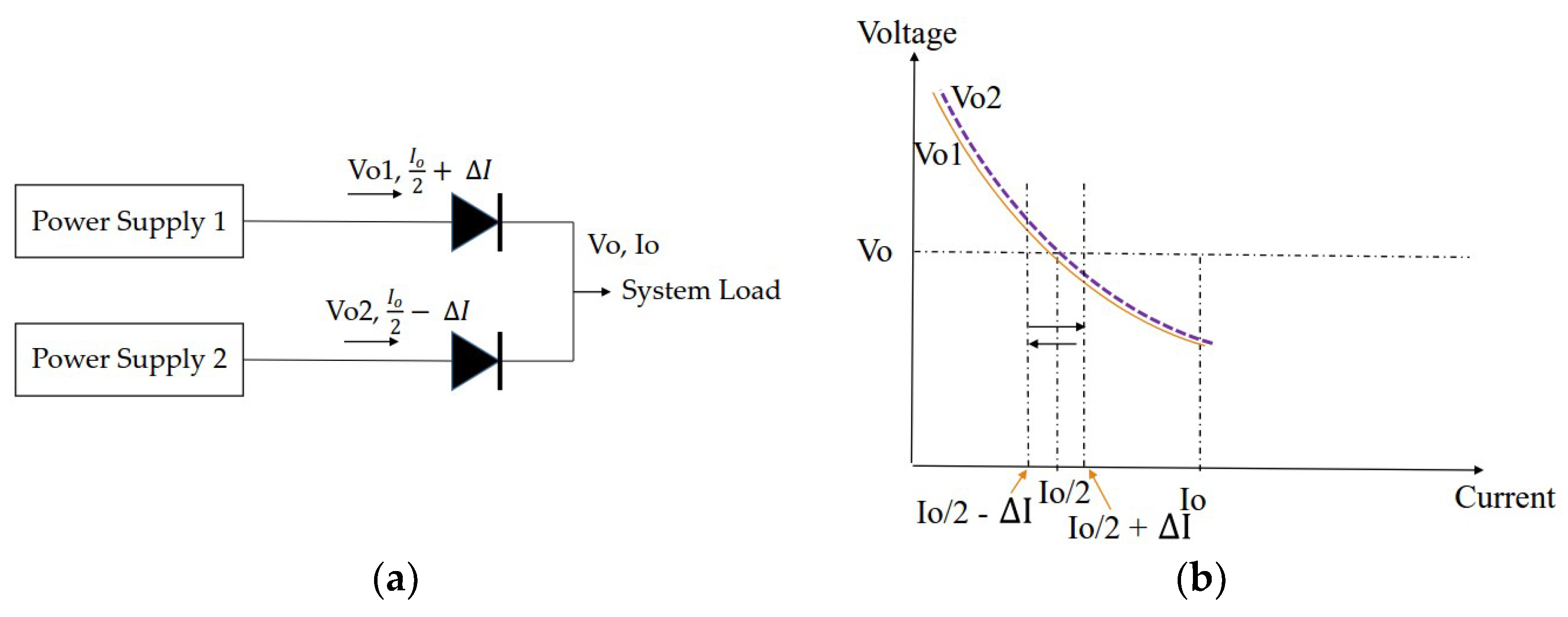
2.1. Voltage Droop via Output Current Feedback

A resistor—which is placed in series with the output—will produce a voltage drop, R si . A block diagram is shown in Figure 2. The output voltage can be expressed as:
V o =   V o i I o i R s i  
where V o i is the output voltage ,   I o i is the output current, V c i is the Pulse Width Modulation (PWM) adjustment signal, and RSi is the resistor series with output load; i is in the range from 1 to N. V s e n s e i = I o i R s i , and each power supply is adjusted by the PWM according to the compensator signals V c i , which were produced by processing V s e n s e i , V o , and V r e f .
The advantages of droop methods are that they are easy to implement, can be combined without any additional current sharing bus, and have high reliability. The disadvantage is that they have worse load regulation.

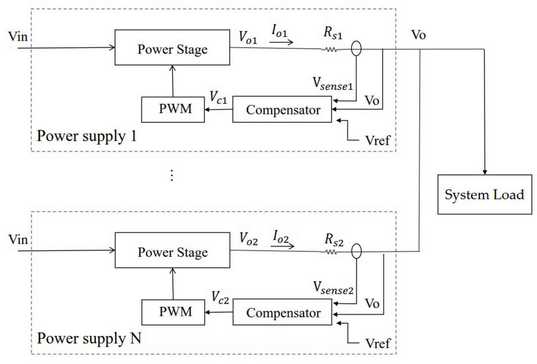
2.2. Outer Loop Regulation

In Figure 3, each power supply has an independent voltage feedback loop and current programming controller. The current programming controller senses the output current signal Vsense1–VsenseN and compares it with a voltage signal produced from a current sharing bus signal passed through a weight circuit [10]. The error signals are Vi1–ViN, which operate with Vo1–VoN and Vref to produce feedback signals for the compensators. The compensators output signals to adjust the duty of PWM. The advantages of this scheme are great modularity, more flexibility for expanding the system, and better fault tolerance of one fault occurring in a single power supply.

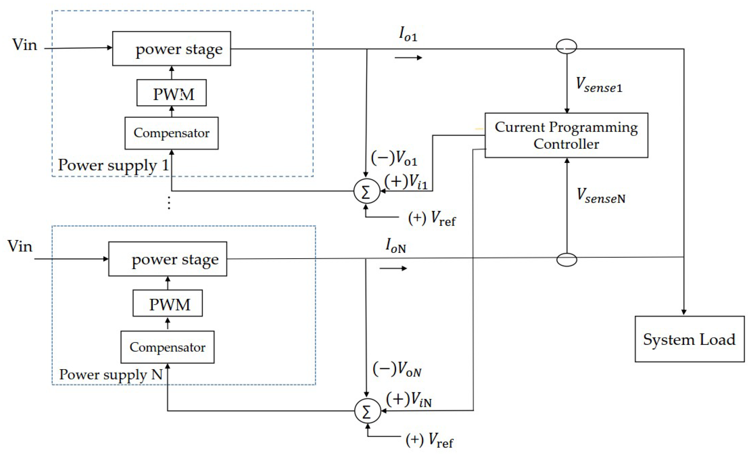
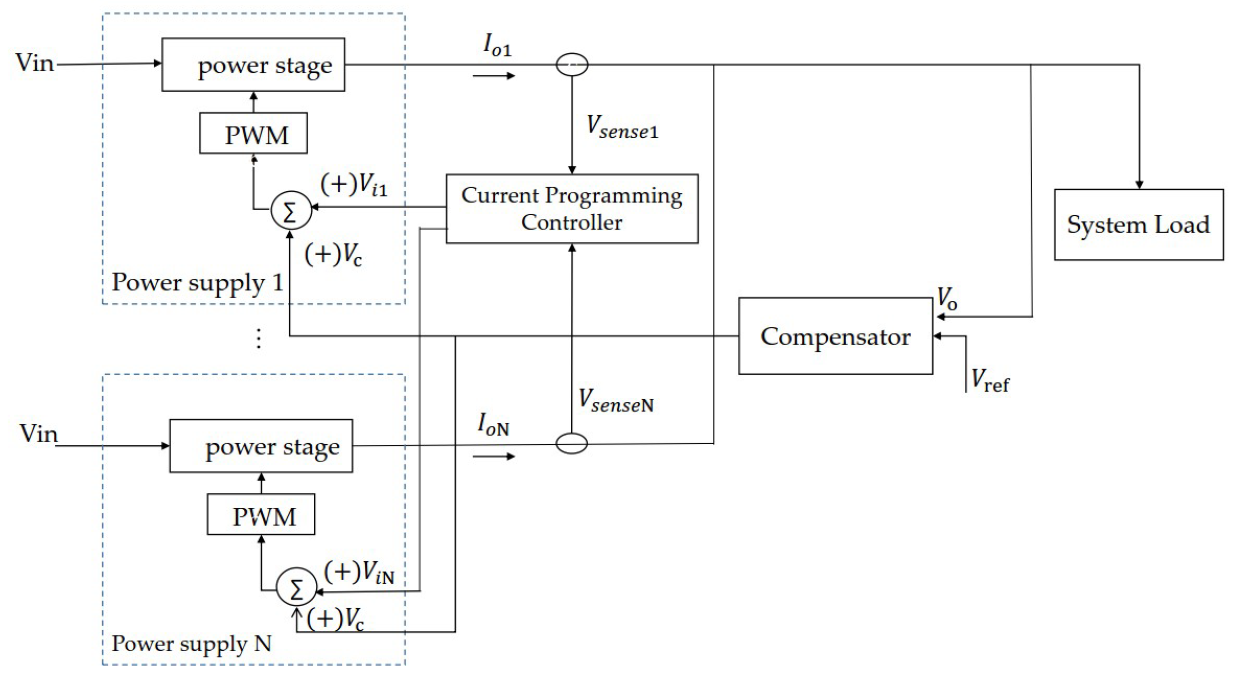
2.3. Inner Loop Regulation

Using the same reference voltage, a voltage feedback loop and compensator can be used to parallel N power supplies. As shown in Figure 4, The PWM generator of each subsystem will be modulated by compensator signal V c and current programming controller signals ( V i 1 V i N ) in order to produce the desired current sharing. The advantages are that signals V s e n s e 1 V s e n s e N do not pass through the compensator, which gives the method a quick response time and makes it more stable than outer loop regulation. The disadvantages are a poor tolerance for fault and less flexibility.

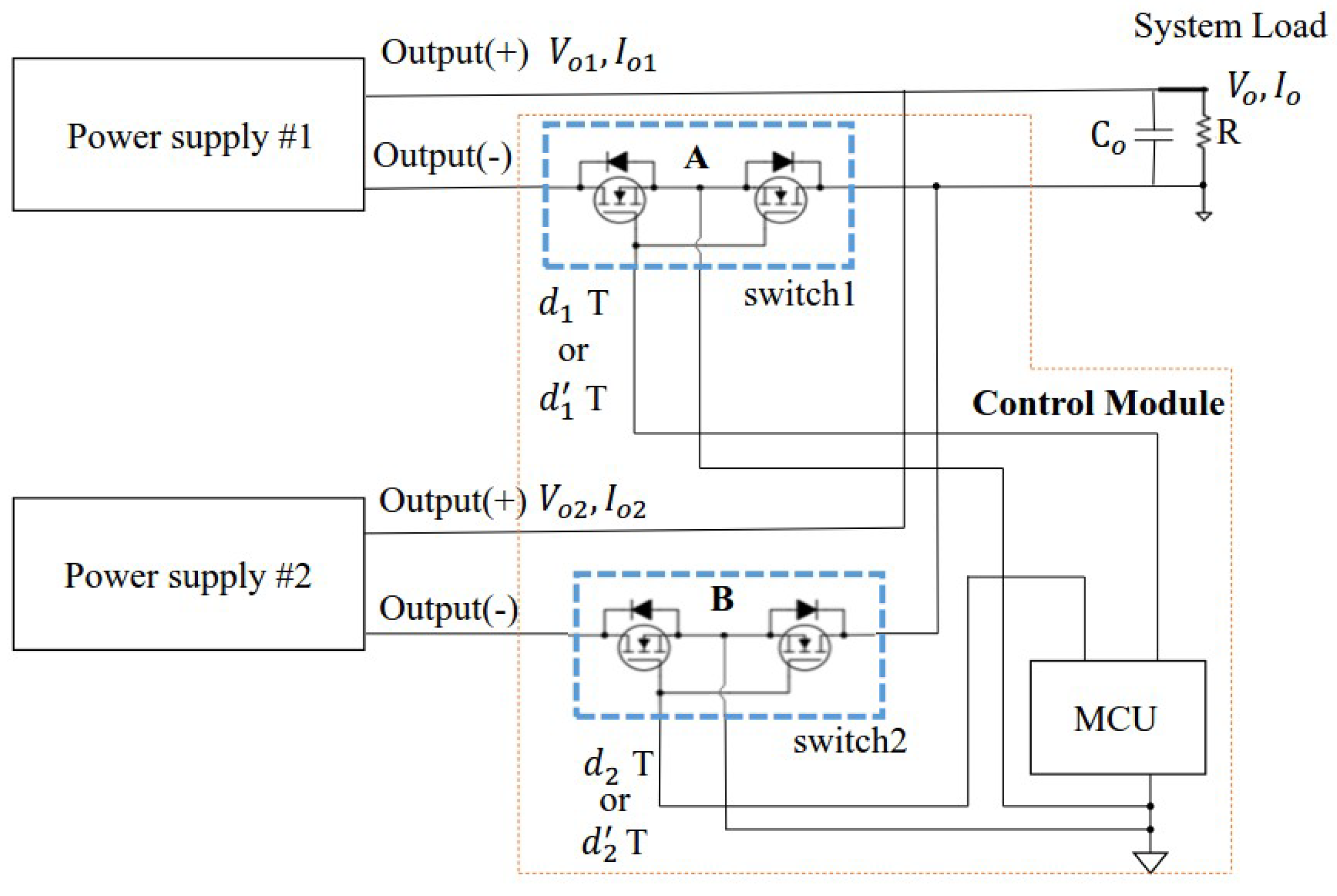
3. The Proposed Architecture

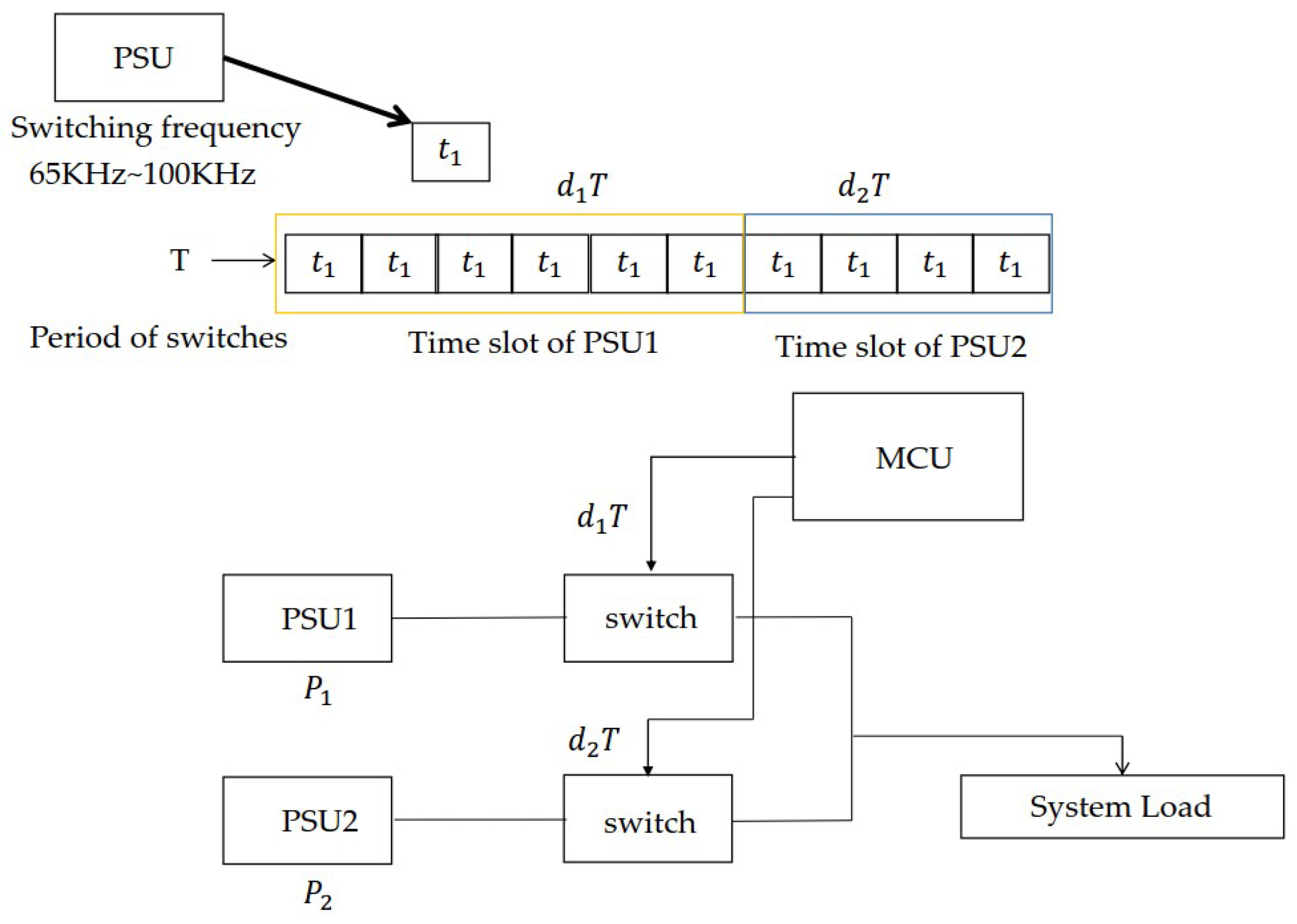
3.1. Architecture of Multi-Phase Switching Method

A current sharing approach for an interleaved flyback micro-inverter was presented by Dong et al. [11]. The multi-phase switching method is another way to use the interleaved method. It can be shown as in Figure 5, in which two different rated power supplies are isolated from the system load through the use of a control module. The output voltages of power supplies 1 and 2 are V o 1 and V o 2 , and their output currents are I o 1 and I o 2 , respectively. The control module includes isolated output switches which are controlled through the direct or overlapped switching method in the micro-programmed controlled unit (MCU). An isolated output switch is composed of two MOSFETs connected back to back [12]. It is important to connect nodes A and B in the MCU to the ground to obtain correct driving voltage.

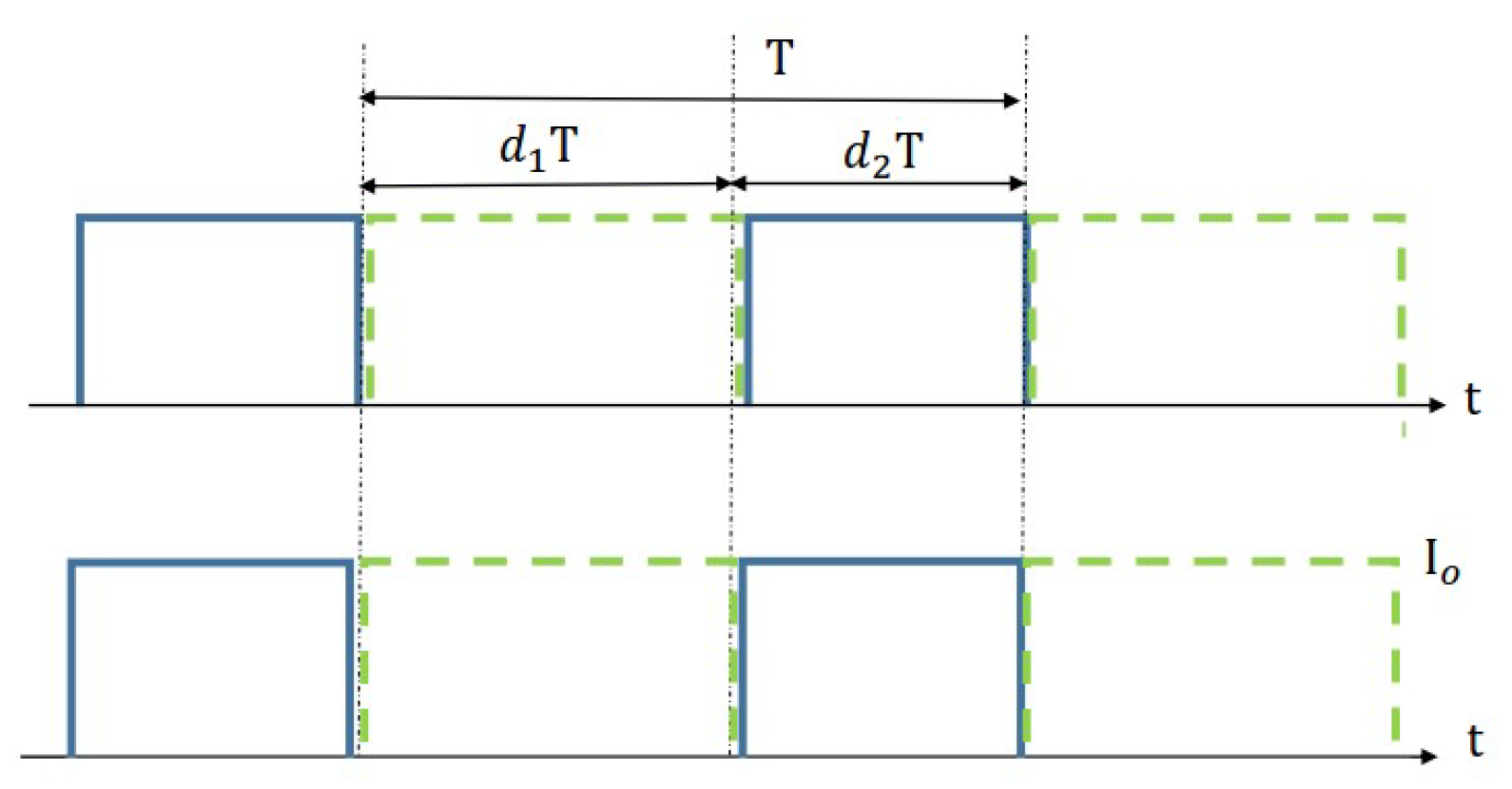
3.2. Direct Switching Method for Multi-Phase Switching

As shown in Figure 6, while switch 1 was turned on, switch 2 was turned off, and vice versa. The period of switches is denoted by T. The duty ( d 1 and d 2 ) while the switches are turned on can be decided according to the rated power of the power supply, as shown in Equations (2)–(4). To avoid the effect of the switching dead time, an output capacitor C o is needed. The equation for calculating C o can be found in Reference [13].
V o I o d 1 = V o 1 I o 1
V o I o d 2 = V o 2 I o 2
d 1 T + d 2 T = T
In setting the period of switches (T), it should be considered that each switching time slot is longer than power supply switching period. As shown in Figure 7, the power supply switching period is t 1 , T is the period of the switches, and the two power supply ratings are P 1 and P 2 . Thus, d 1 : d 2 = P 1 : P 2 . A simple means of meeting the requirement for setting the multi-phase switching period is setting T equal to 10 × t 1 .

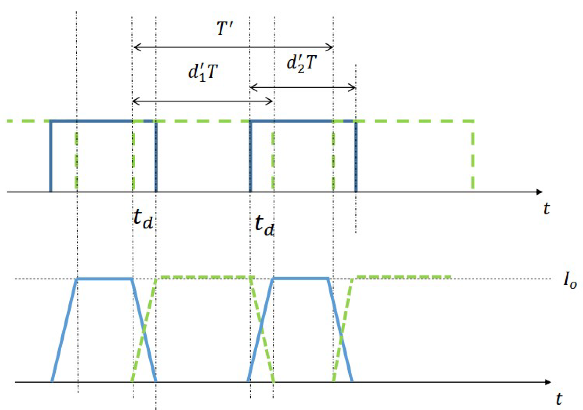
3.3. Overlapped Switching Method for Multi-Phase Switching

In this method, the first step is to decide the overlapping time, t d . As shown in Figure 8, the period of switches is denoted by T’, which equals T 2 t d . Except for the overlapping time period, power supplies individually supply power ( V o I o ) to the system load in their own time slots. The new switching duty ratio is calculated as d 1 T t d   :   d 2 T t d . While d 1 T > 10 t d and d 2 T > 10 t d , the new switching duty ratio will be approximately d 1 T :   d 2 T . This is equal to the direct method. Instead of switching dead time, the switches are turned on during overlapping. Therefore, output capacitor C o can be removed.

3.4. Comparison of Conventional Methods and Multi-Phase Switching Methods

Table 1 provides a comparison of conventional and multi-phase switching methods. The merits and disadvantages of conventional methods were presented by Luo et al. [10]. The voltage droop method is easy to implement but provides poor current-sharing. Inner and outer loop regulation perform better at current sharing but require a current sharing bus and a suitable design for a feedback circuit. Multi-phase switching methods are realized by an external module that is controlled by an MCU. In such methods, it is easy to realize parallel power supplies and reduce power dissipation produced by the ORing diode. The requirements for multi-phase switching methods are a strict switching sequence and the capability of peak power for a power supply. The peak power rating of a power supply limits the paralleling power rating. For example, 60 W power supply outputs 150 W for hundreds of microseconds. This means that 60 and 90 W power supplies can be paralleled together. If a 60 W power supply can output 300 W for hundreds of microseconds, 60 and 240 W power supplies can be paralleled together.

3.5. Applications

The proposed methods have modularity and are flexible for paralleling power supplies. The possible applications are included in wireless sensor networks and the Internet of things. For example, a wireless sensor network increased by more sensors will need a larger power supply. One way to solve this problem is to replace the original power supply. Another way is to reuse the original power supply and parallel another power supply by the methods presented in this paper. Therefore, the proposed method is more flexible for the reusing of power supplies. The authors of References [1,14,15] presented the paralleling of power sources of wireless sensor networks. The proposed method can use a new power source only by adding more isolated MOSFETs and re-assigning the on-time of each isolated MOSFET. As shown in Reference [16], two kinds of operating modes—sleep mode and active mode—will save the energy of Internet of Things nodes by changing these two states. The proposed method can change the on-time sequence of isolated MOSFETs to achieve this requirement.

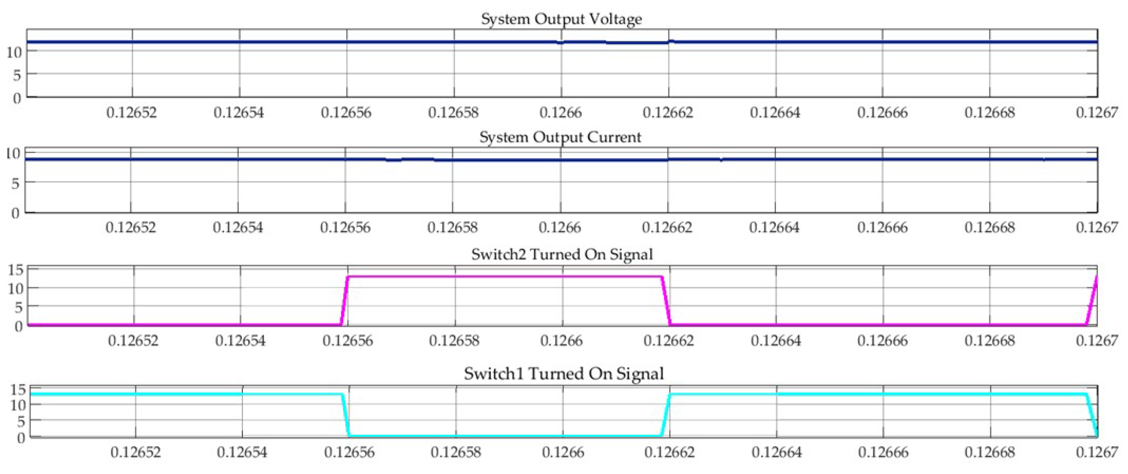
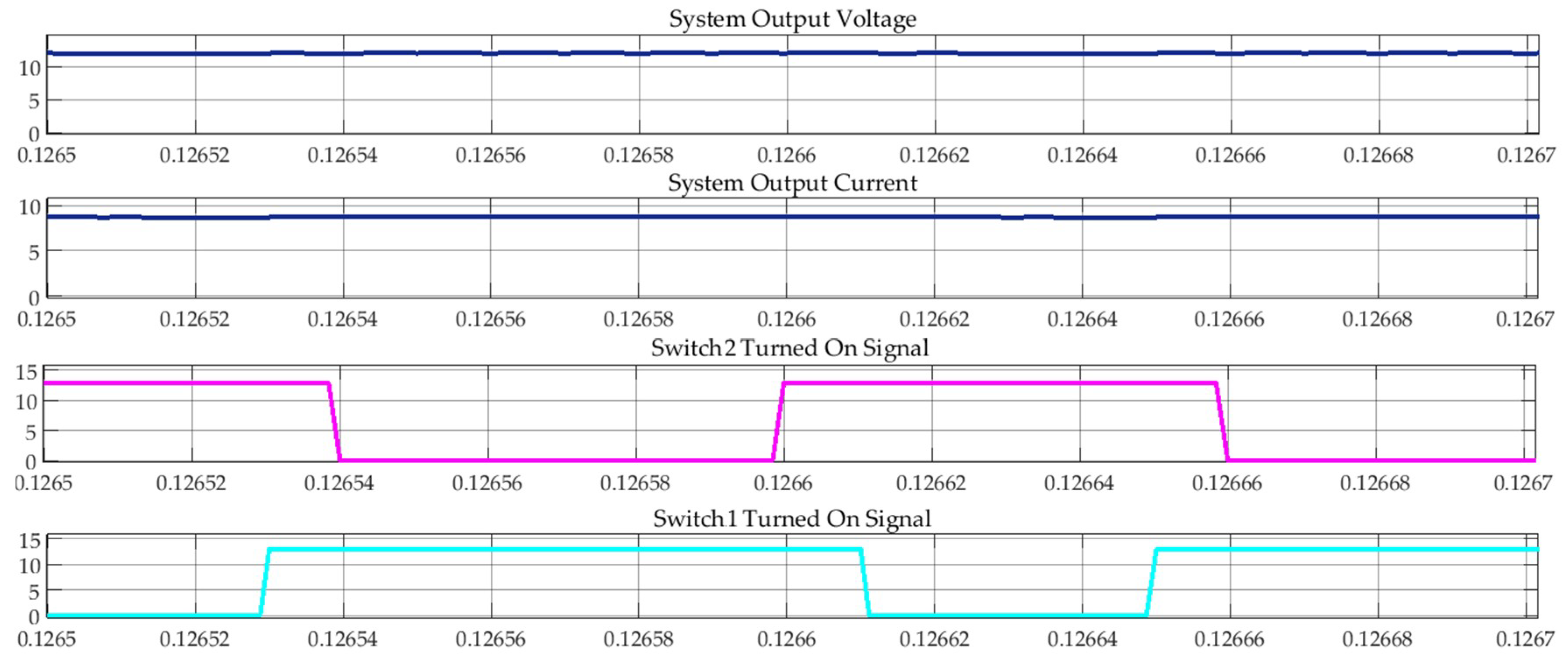
3.6. Simulation Results

The simulations were processed using MATLAB Simulink, in which two rated power supplies (60 and 45 W) were used. The period (T) was 140 μ s, d 1 = 0.57 , and d 2 = 0.43 . The output voltage was 12 V. As shown in Figure 9, the switch-based signals were turned on in different time slots. Thus, dead time existed while the states of the switches were changing. To overcome the effect of dead time, an output capacitor is needed. After paralleling a 47 μ F output capacitor, the system voltage and the system load performed normally.
As shown in Figure 10, the overlapping time is 10 μ s and the new period ( T ) is 120 μ s; the switching duty ratio is approximately 0.58:0.42. The system voltage and system load also performed normally without paralleling an output capacitor.

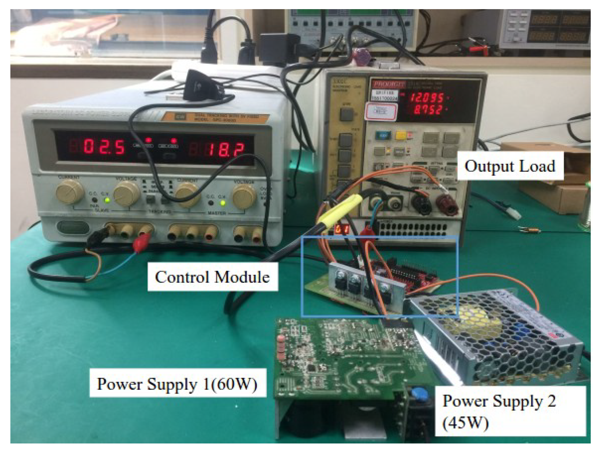
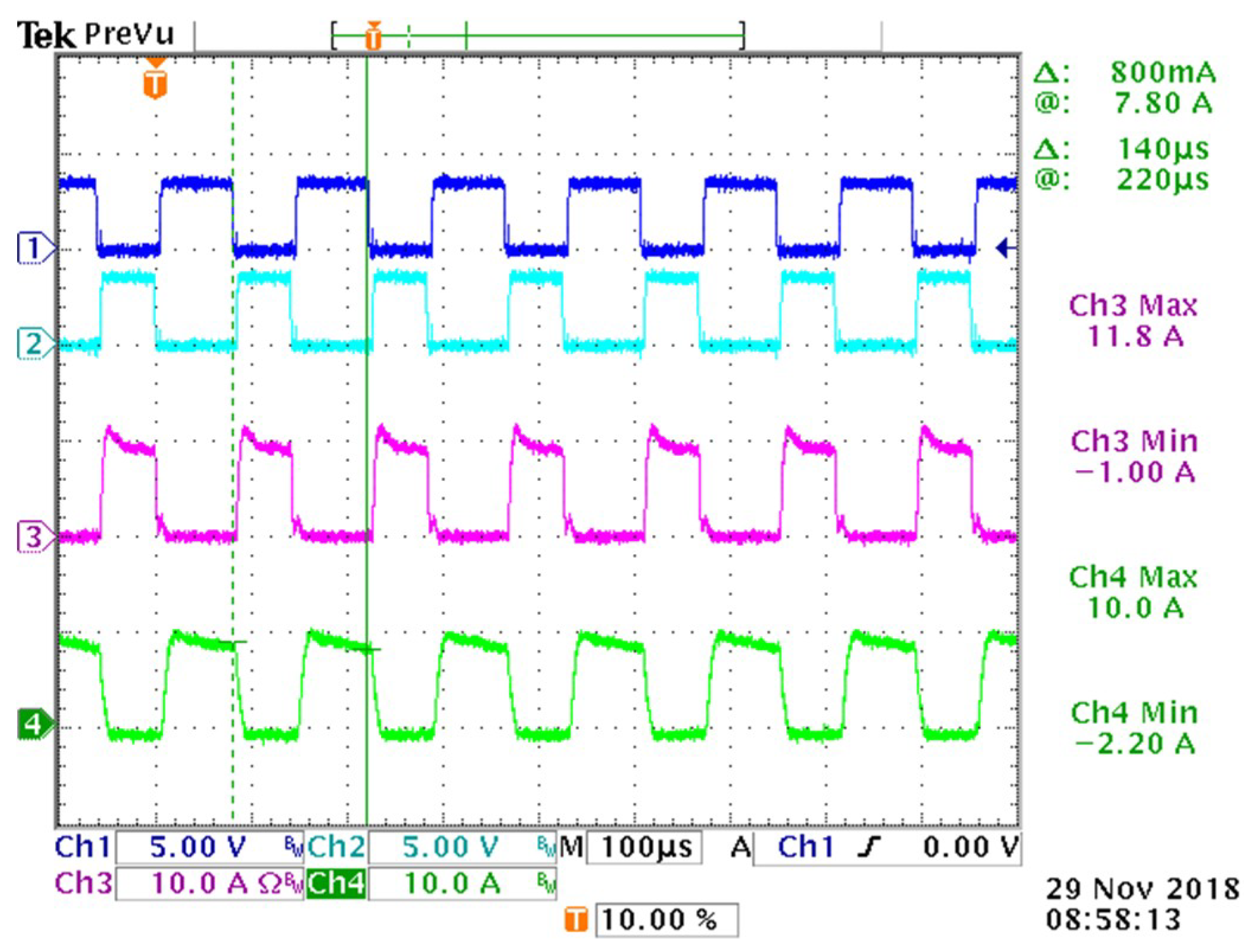
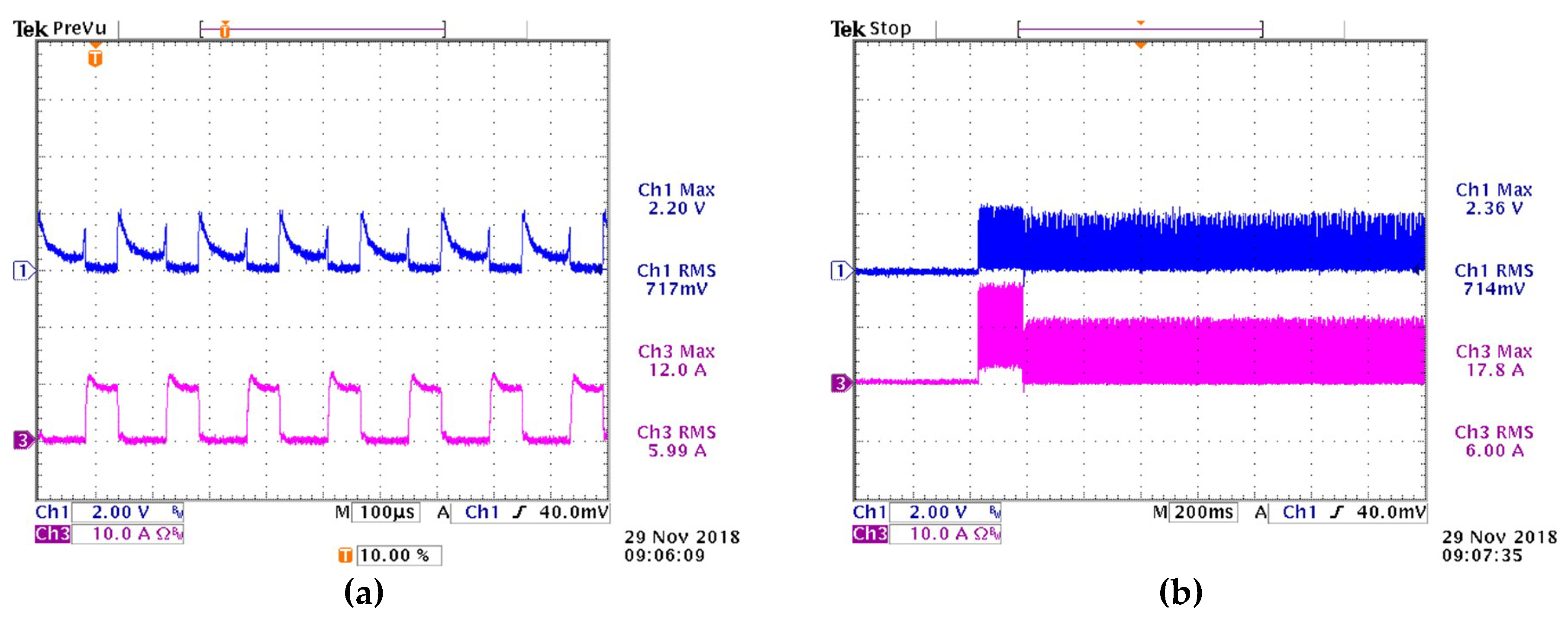
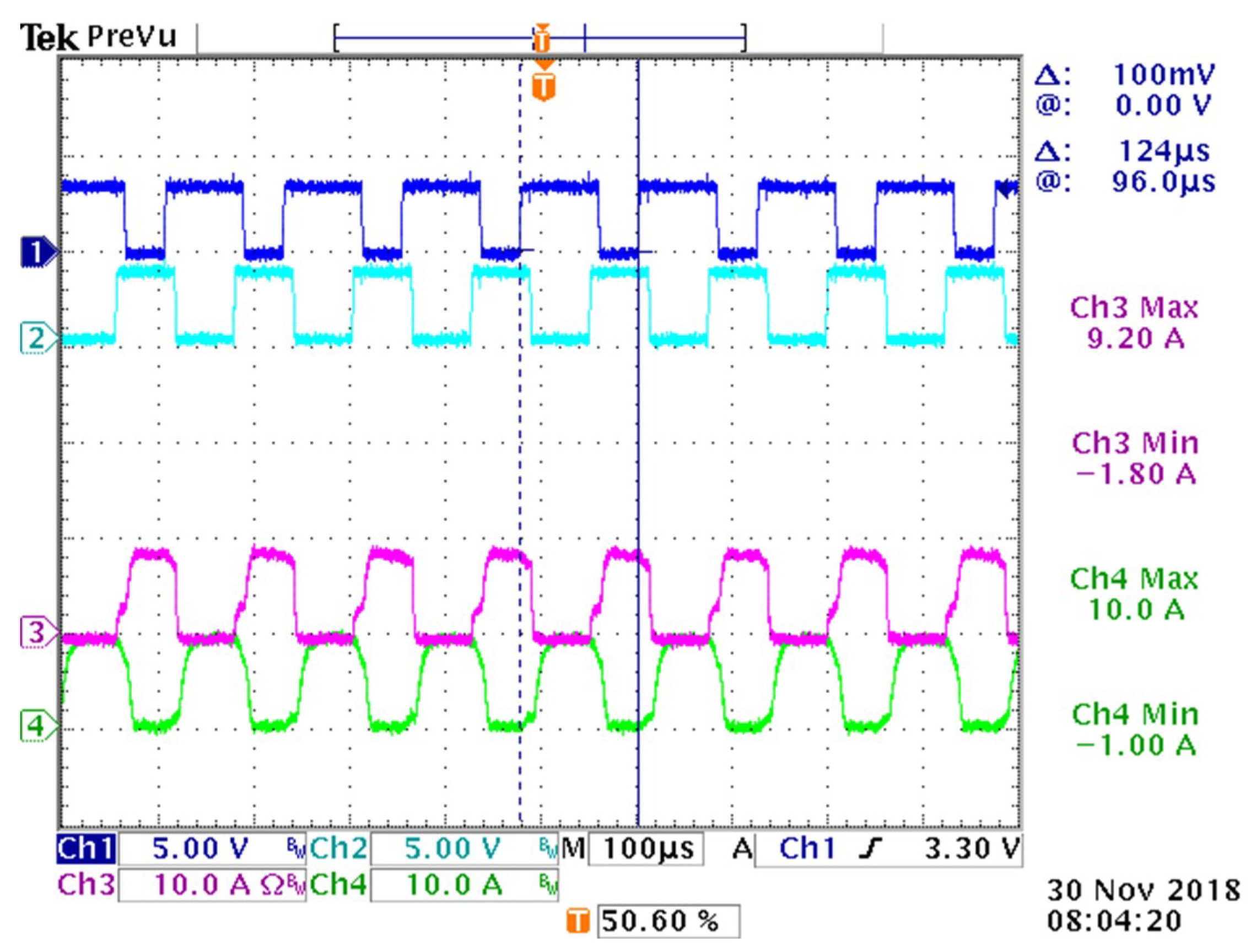
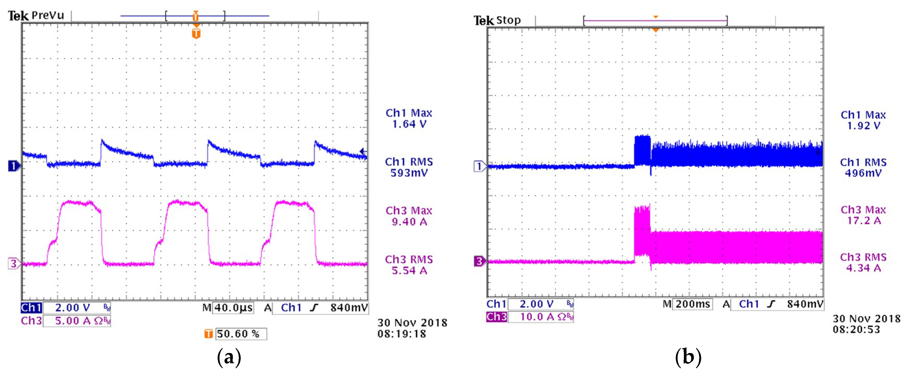
3.7. Experimental Results

Figure 11 shows the use of power supply 1 (60 W) and power supply 2 (45 W). The MCU of the control module is MSP430G2553, and the MOSFETs are STP80NF55. The output switching period (T) was 140 μ s, and the output load was 12 V at 8.75 A. The switching frequency of power supplies was approximately 65 KHz. Therefore, the period is about 15.3 μ s ; thus, each output switching time slot needed to be longer than 15.3 μ s. To make sure that each time slot was longer than 15.3 μ s and that it was easy to assign the time slots for each power supply, 140 μ s was set. For the direct switching method, an output capacitor of 47 μ F was used. For the overlapped switching method, however, the output capacitor of 47 μ F was removed, and the overlapping time of the control module was set to 10 μ s in order for the switching duty ratio to be similar to that of the direct method.
Figure 12 depicts two power supplies paralleled by the direct switching method. Channels 1 and 2 are gate signals of switches, and channels 3 and 4 are current passed through switches while switches were turned on. When the channel 1 signal was high, channel 4 represented the current passed through the switch connected to power supply 1 in series. When channel 2 signal was high, channel 3 represented the current passed through the switch connected to power supply 2 in series. For the direct switching method, there is a higher transient peak current that may cause a higher output ripple. Therefore, more output capacitors are needed.
Figure 13a shows the stress on the switch in the steady state. Channel 1 is the switch   V d s , and channel 2 is the current passed through the switch. The maximum V d s is 2.2 V, and the maximum current is 12 A. Figure 13b shows the transient state. Channel 1 is the switch V d s , and channel 2 is the current passed through the switch. The maximum V d s is 2.36 V, and the maximum current is 17.8 A. The voltage stress on the switch is small. Thus, the current stress on the switch needs to be considered. According to the specification of MOSFETs, STP80NF55 can support 80 A passed through it, and the voltage rating is 55 V. Therefore, the results are under the rated stress.
Figure 14 depicts two power supplies paralleled by the overlapped switching method. Channels 1 and 2 are gate signals of switches, and channels 3 and 4 are current passed through switches while switches were turned on. When the channel 1 signal was high, channel 4 represented the current passed through the switch connected to power supply 1 in series. When channel 2 signal was high, channel 3 represented the current passed through the switch connected to power supply 2 in series. For the overlapped switching method, the transient current was smooth. Therefore, the output capacitors could be removed.
Figure 15a shows the stress on the switch in the steady state. Channel 1 is the switch V d s , and channel 2 is the current passed through the switch. The maximum V d s is 1.64 V, and the maximum current is 9.4 A. Figure 15b shows the transient state. Channel 1 is the switch V d s , and channel 2 is the current passed through the switch. The maximum V d s is 1.92 V, and the maximum current is 17.2 A. According to the specification of MOSFETs, these results are under the rated stress.
For the direct switching method, the input power was 126.8 W, the output voltage was 11.6 V, and the output current was 8.75 A. Thus, the efficiency was 0.8. For the overlapped switching method, the input power was 125.3 W, the output voltage was 11.6 V, and the output current was 8.75 A. Thus, the efficiency was 0.81. Therefore, the efficiency for the direct switching and overlapped switching method was similar.

4. Conclusions

This paper proposed the modularity for paralleling power supplies with different rated powers by using multi-phase switching methods. To divide the output switching period into several time slots conveniently, the output switching period was set to 10 times the power supply switching period. To neglect the difference of duty between the direct and overlapped switching methods, the overlapping time was set smaller than the switching frequency of the power supply. As in Reference [1], using a power ORing will produce more power dissipation. Multi-phase switching methods replace the power ORing with MOSFETs, which reduce power dissipation and can also be isolating components. This makes it possible to achieve different rated power supplies in parallel without adding a circuit to the power supplies.

Author Contributions

P.-H.L. is the main author and is responsible of the design and for writing the paper. Y.-T.C. and F.-R.C. provided valuable suggestions during the design phase and also while preparing the manuscript.

Funding

This research received no external funding.

Conflicts of Interest

The authors declare no conflict of interest.

References

  1. Estrada-López, J.J.; Abuellil, A.; Zeng, Z.; Sánchez-Sinencio, E. Multiple Input Energy Harvesting Systems for Autonomous IoT End-Nodes. J. Low Power Electron. Appl. 2018, 8, 6. [Google Scholar] [CrossRef]
  2. Chiang, H.C.; Jen, K.K.; You, G.H. Improved droop control method with precise current sharing and voltage regulation. IEEE Trans. Circuits Syst. Video Technol. 2016, 26, 1334–1349. [Google Scholar] [CrossRef]
  3. Su, J.T.; Lin, C.W. Auto-tuning scheme for improved current sharing of multiphase DC-DC converters. IET Power Electron. 2012, 5, 1605–1613. [Google Scholar] [CrossRef]
  4. Panov, Y.; Rajagopalan, J.; Lee, F.C. Analysis and design of N paralleled DC-DC converters with master-slave current-sharing control. In Proceedings of the 21th Annual IEEE Applied Power Electronics Conference and Exposition, Atlanta, GA, USA, 27 February 1997; Volume 1, pp. 436–442. [Google Scholar]
  5. Wildrick, C.M.; Lee, F.C.; Cho, B.H.; Choi, B.C. A method of defining the load impedance specification for a stable distributed power system. IEEE Trans. Power Electron. 1995, 10, 280–285. [Google Scholar] [CrossRef]
  6. Cheng, D.K.; Lee, Y.S.; Chen, Y. A current-sharing interface circuit with new current-sharing technique. IEEE Trans. Power Electron. 2005, 20, 35–43. [Google Scholar] [CrossRef]
  7. Zhang, X.; Crradini, L.; Maksimovic, D. Sensorless Current Sharing in Digitally Controlled Two-Phase Buck DC-DC Converters. In Proceedings of the 24th Annual IEEE Applied Power Electronics Conference and Exposition, Washington, DC, USA, 15–19 February 2009; pp. 70–76. [Google Scholar]
  8. Wang, J.B.; Lee, J.H.; Kao, D. Control and analysis of the low voltage DC grid. In Proceedings of the International Future Energy Electronics Conference, Tainan, Taiwan, 3–6 November 2013; pp. 800–805. [Google Scholar]
  9. You, J.; Wang, H.; Meng, F.R.; Cui, J.W. Analysis of Current Sharing and Controller Design Fundamental for Paralleled DC/DC Power Converters. In Proceedings of the IEEE International Conference on Information and Automation, Harbin, China, 20–23 June 2010; pp. 555–558. [Google Scholar]
  10. Luo, S.G.; Ye, Z.H.; Lin, R.L.; Lee, F.C. A classification and evaluation of paralleling methods for power supply modules. In Proceedings of the 30th Annual IEEE Power Electronics Specialists Conference, Charleston, SC, USA, 1 July 1999; Volume 2, pp. 901–908. [Google Scholar]
  11. Dong, M.; Tian, X.; Li, L.; Song, D.; Wang, L.; Zhao, M. Model-Based Current Sharing Approach for DCM Interleaved Flyback Micro-Inverter. Energies 2018, 11, 1685. [Google Scholar] [CrossRef]
  12. Daowd, M.; Antoine, M.; Omar, N.; Lataire, P.; van den Bossche, P.; van Mierlo, J. Battery Management System—Balancing Modularization Based on a Single Switched Capacitor and Bi-Directional DC/DC Converter with the Auxiliary Battery. Energies 2014, 7, 2897–2937. [Google Scholar] [CrossRef] [Green Version]
  13. Diab, Y.; Venet, P.; Gualous, H.; Rojat, G. Self-discharge characterization and modelling of electrochemical capacitor used for power electronics applications. IEEE Trans. Power Electron 2009, 24, 510–517. [Google Scholar] [CrossRef]
  14. Li, Y.; Yu, H.; Su, B.; Shang, Y. Hybrid Micropower Source for Wireless Sensor Network. IEEE Sens. J. 2008, 8, 678–681. [Google Scholar] [CrossRef]
  15. Fukushima, Y.; Fukuma, M.; Yoshino, K.; Kishida, S.; Lee, S. A KOH Solution Electrolyte-Type Electric Double Layer Supercapacitor for a Wireless Sensor Network System. IEEE Sens. 2018, 2, 1–4. [Google Scholar] [CrossRef]
  16. Grasso, A.D.; Palumbo, G.; Pennisi, S. Switched-Capacitor Power Management Integrated Circuit for Autonomous Internet of Things Node. IEEE Trans. Circuits Syst. II Express Briefs 2018, 65, 1455–1459. [Google Scholar] [CrossRef]
Figure 1. Supplying power by paralleling power supplies: (a) represents the block diagram of paralleling power supplies, and (b) represents the relationship of output voltage and output current while paralleling power supplies.
Jlpea 09 00001 g001
Figure 2. Paralleling power supplies by voltage droop method.
Jlpea 09 00001 g002
Figure 3. Outer loop regulation for paralleling power supplies.
Jlpea 09 00001 g003
Figure 4. Inner loop regulation for paralleling power supplies.
Jlpea 09 00001 g004
Figure 5. Modularity for paralleling different rated power supplies by using a multi-phase switching method.
Jlpea 09 00001 g005
Figure 6. Signals of switch gate driving and output current of each power supply in different time slots for the direct switching method. The dashed line represents power supply 1, and the solid line represents power supply 2. I o denotes the system load.
Jlpea 09 00001 g006
Figure 7. Setting the period of switches.
Jlpea 09 00001 g007
Figure 8. Signals of switch gate driving and output current of each power supply in different time slots for the overlapped switching method. The dashed line represents power supply 1, and the solid line represents power supply 2. I o denotes the system load.
Jlpea 09 00001 g008
Figure 9. Simulation results of the direct switching method for 60 and 45 W power supplies.
Jlpea 09 00001 g009
Figure 10. Simulation results of the overlapping switching method for 60 and 45 W power supplies.
Jlpea 09 00001 g010
Figure 11. Paralleling different rated power supplies by multi-phase switching methods in a control module.
Jlpea 09 00001 g011
Figure 12. The switches’ driving signals and the output current of power supplies by the direct switching method.
Jlpea 09 00001 g012
Figure 13. The stress on the switch by the direct switching method: (a) the stress in the steady state and (b) the stress in the transient state.
Jlpea 09 00001 g013
Figure 14. The MOSFETs driving signals and the output current of power supplies by the overlapped switching method.
Jlpea 09 00001 g014
Figure 15. The stress on MOSFETs by the overlapped method: (a) the stress in the steady state and (b) the stress in the transient state.
Jlpea 09 00001 g015
Table 1. Comparison of voltage droop method, inner loop regulation, outer loop regulation, and multi-phase switching method.
MethodsMeritsdisadvantages
Voltage droop
  • Easy to implement
  • Does not need current sharing bus
  • High modularity
  • Degrading load regulation
  • Poor current-sharing due to open loop for parallel system
Inner loop regulation
  • Stable current sharing
  • Precise output voltage regulation
  • Degrades the modularity of the system
  • Poor fault tolerance
  • Needs current sharing bus
Outer loop regulation
  • Good modularity and standardization for manufacturing
  • Flexibility in system configuration—easy to expand and maintain the system
  • Excellent fault tolerance against the failure of any single module
  • Possibly unstable in transient
  • Needs current sharing bus
Multi-phase switching
  • Flexibility in system configuration, easy to expand
  • Paralleling possible without current sharing bus
  • Replaces isolated diode with isolated MOSFETs to reduce power dissipation
  • Requires strict switching sequence
  • The paralleling power rating is limited by power supply

