
Microwave Atom Chip Design


Department of Physics, College of William and Mary, 300 Ukrop Way, Williamsburg, VA 23187, USA
*
Author to whom correspondence should be addressed.
Atoms 2021, 9(3), 54; https://0-doi-org.brum.beds.ac.uk/10.3390/atoms9030054
Submission received: 16 June 2021
/
Revised: 24 July 2021
/
Accepted: 30 July 2021
/
Published: 5 August 2021
(This article belongs to the Special Issue Atomic Interferometry with Bose–Einstein Condensates)
Abstract
:We present a toolbox of microstrip building blocks for microwave atom chips geared towards trapped atom interferometry. Transverse trapping potentials based on the AC Zeeman (ACZ) effect can be formed from the combined microwave magnetic near fields of a pair or a triplet of parallel microstrip transmission lines. Axial confinement can be provided by a microwave lattice (standing wave) along the microstrip traces. Microwave fields provide additional parameters for dynamically adjusting ACZ potentials: detuning of the applied frequency to select atomic transitions and local polarization controlled by the relative phase in multiple microwave currents. Multiple ACZ traps and potentials, operating at different frequencies, can be targeted to different spin states simultaneously, thus enabling spin-specific manipulation of atoms and spin-dependent trapped atom interferometry.
1. Introduction
Trapped atom interferometers provide a spatially localized sample and potentially long coherent phase interrogation times in packages as compact as an atom chip. These benefits make them strong candidates for precision inertial navigation (i.e., acceleration and rotation sensing), gravimetry, and microscopy, e.g., sub-mm gravity and Casimir–Polder measurements. These benefits also come at the cost of increased atom–atom interactions, which can reduce the accuracy of the interferometer. Operating the interferometer with a Bose–Einstein condensate with low atom numbers can mitigate interactions [1] at the cost of reduced signal. Alternatively, operating with degenerate fermions should suppress interactions [2,3], and ultracold thermal bosons should also experience lower interactions.
A trapped atom interferometer based on degenerate fermions or ultracold thermal bosons is similar to a white light interferometer and must ensure a state-independent beamsplitting phase to avoid washing out the fringes [4,5]. One solution is to use two overlapping identical spin-specific traps for two different spin states that are spatially separated, follow different paths, and then recombined, i.e., a Ramsey interferometer with spatially separated spin states. Such an approach requires the spin-specific microwave traps that are the focus of this paper.
Unfortunately, spin-specific potentials are not part of the standard toolbox of ultracold atom trapping. DC Zeeman potentials are spin-dependent and modify the energy of all spins in a proportional manner; optical dipole potentials can be engineered to include a spin-dependence but at the cost of significant spontaneous emission heating [6]. Fortunately, the AC Zeeman (ACZ) effect, based on microwave hyperfine transitions, offers a clear mechanism for spin-specific control of atoms [7]. However, strong microwave gradients on length scales much shorter than the wavelength are needed for trapping, so microwave near fields generated by atom chip currents must be employed.
The use of high-frequency currents has a transformative effect on the capabilities of chip traps by introducing two new control parameters: frequency (as detuning) to control the ACZ strength and polarity, and relative phase between wire currents to control the circularly-polarized field shape. Furthermore, ACZ traps can operate at any background magnetic field, , and can turn any hyperfine substate into a high- or a low-field seeker, as we explain below.
This paper presents the basic building blocks for designing a microwave atom chip based on microstrip transmission lines that can trap atoms via spin-specific ACZ potentials. In Section 2, we present the basic two-level theory of the ACZ effect for microwave transitions between hyperfine manifolds. In Section 3, we introduce basic physical considerations for using microstrip transmission lines, our proposed building block. Section 4 discusses useful trap geometries based on two- and three-microstrip simplified models. Section 5 presents numerical simulations of the trapping near field generated by two- and three-microstrip geometries. Section 6 shows how a standing wave microwave lattice can be used for axial confinement along the length of a trace. We conclude in Section 7 and provide an outlook for future work.
2. Two-Level AC Zeeman Theory
Consider an atom with hyperfine spin states and separated by energy to which we apply a microwave magnetic field, . If the field contains N microwave photons and oscillates with frequency , then working with the bare states [8,9], , the Hamiltonian for the system is given by
where the Rabi frequency is . The Rabi frequency is an important parameter, scaling the strength and linewidth of the ACZ interaction and selecting relevant field polarizations. Neglecting the nuclear spin , the ground state () atom’s magnetic moment is the valence electron spin, given as , where is the Bohr magneton ( = 9.2740100783(28) × 10−24 J/T [10]), is the spin operator of the electron, and is the electron gyromagnetic factor, which we take to be here. Working in the circular polarization basis and taking to be the quantization direction, we can express the Rabi frequency as
where are the spin raising and lowering operators and . The first two terms represent the transitions for circularly polarized AC magnetic fields, and the last term represents transitions. These matrix elements for the inter- and intra-manifold transitions are calculated in Appendix A. In our application, the spatial shape of the Rabi field field gives the entire trapping gradient, as and are intended to be global parameters.
By subtracting the offset , the Hamiltonian simplifies to
where the detuning is defined as . This dressed atom Hamiltonian can also be obtained by considering a two-level system interacting with an oscillating magnetic field and making the appropriate rotating frame transformation and rotating wave approximation [11]. The detuning has a moderating effect on the ACZ energy shift and trapping potential shape off-resonance, and it defines the degree of state mixing near resonance. We illustrate the role of detuning on trap shape in Figure 1d for a sample two-microstrip trap, explained later (see Section 5.1). Since the Rabi frequency broadens resonances, provides a good dimensionless parametric handle on the system.
The eigenenergies and eigenstates of this Hamiltonian are
where , , and . The ACZ energy shift, determined by how the energies of the states differ from the bare state energies, is given by
By implementing an adiabatic rapid passage sweep, either of the bare atomic states can be made into a low- or high-field seeking state based on the initial detuning, as shown in Figure 1a,b.
Notably, the () state increases (decreases) in energy in the presence of a microwave field, so it is a low- (high-) field seeker. Since microwave near fields cannot have a local field maximum via Earnshaw’s theorem, any ACZ near field trap is based on a microwave minimum to trap atoms in the low-field seeking state.
Recalling the form of Ω from Equation (3) and the ACZ energy in Equation (8), we highlight the dependence on frequency and polarization of the applied microwave field as well as the states and . By tuning these parameters, the potential can be made to trap targeted spin states. The addition of a sufficiently large static field results in increased splitting between hyperfine states, causing neighboring states to become less affected by the potential via detuning isolation. In the far off-resonance limit , the two states resemble the bare atomic states and hardly mix. The ACZ energy shift for the two states is given by , where the plus corresponds to and the minus corresponds to . Near resonance , the eigenstates of the dressed Hamiltonian are roughly equal superpositions of the bare states. In this limit the energy shift is . We note that near resonance, the energy shift scales linearly with the strength of the applied field (encoded in ). As we move off-resonance, the relationship becomes quadratic. These limits are shown in Figure 1c. The near resonance approximation is well-matched to the exact energy shift for , while the far off-resonance limit is a good description of the energy shift when .
We can visualize the role of detuning on the shape of the ACZ trap by plotting the vertical trap profile for a two-microstrip configuration (see Section 5.1) at various detunings, shown in Figure 1d. The ACZ potential is plotted in μK, based on , where is Boltzmann’s constant. On resonance (), we see the expected linear profile in the vicinity of the potential minimum. As detuning is increased, the trap becomes harmonic over a larger region and flattens out.
3. Microstrip-Based Atom Chip Design
The primary purpose of a microwave atom chip is to generate microwave and RF near fields with strong enough gradients to generate a substantial ACZ trapping force. In the near field, the spatial scale for field variations is determined by the chip’s wire spacings and wire widths (not the wavelength), so the chip’s basic architectural building blocks should have small wire widths and be compatible with small inter-wire spacings.
In this paper, we present chip trap designs based on microstrip transmission lines [14] because they have two key features: (1) microstrips can have relatively small trace widths and spacings, and (2) their simple and extended microwave field mode is well suited to generating trapping potentials. In contrast, while co-planar waveguide (CPW) transmission lines have been used in microwave atom chips [15,16], their compact and double-lobed field structure makes trap design more challenging. Alternatively, the negative index of refraction metamaterial lenses represent a tantalizing prospect for generating compact microwave trapping structures but are beyond the scope of this paper [17].
Microstrip transmission lines consist of a conducting trace on a planar dielectric substrate with a conducting ground plane on the opposite side. Figure 2 shows the layout and dimensions of the 50 microstrip that is the basic building block for the chip trap designs in this paper (presented in the next sections). We choose a 50 Ω impedance in order to facilitate impedance matching with the 50 Ω standard used in microwave cables, amplifiers, and sources. In order to achieve both a 50 Ω impedance and a narrow trace width, a thin substrate with a high dielectric constant is required [18,19]. Aluminum nitride (AlN, dielectric constant 8.9) additionally has a high thermal conductivity to facilitate heat dissipation at high microwave power. To realize the desired impedance at 6.8 GHz with a 50 μm thick AlN substrate, we find that a 54 μm wide copper trace optimizes the transmission of microwaves through the microstrip.
The microwave field mode propagating through the microstrip is quasi-TEM (transverse electro-magnetic), where the “quasi” is due to a small longitudinal electric component (generally negligible) that arises from the vacuum–substrate interface. The thin-substrate microstrip of Figure 2 has good broadband performance (i.e., largely frequency independent), which extends past 20 GHz according to our numerical simulations. Furthermore, a single microstrip can support multiple, simultaneous, independent microwave near fields at different frequencies, with each one targeted to a different spin state.
The basic structure of the microstrip’s field mode can be understood to arise from the current and charge on the trace and from the opposing current and charge on the “mirror trace” expected from the method of images (see Figure 2): a static analysis yields a decent estimate of the magnetic and electric near fields (for distances much smaller than the wavelength) and can be converted to a time-dependent field by multiplying by , i.e., and . Section 4 uses this analysis to understand the trap position for various wire and microstrip configurations.
Numerical simulations are needed to obtain accurate estimates of the microstrip’s near field mode. In particular, at high frequencies, the current tends to hug the trace edges due to the AC skin effect [20], which in turn tends to modify the near field at distances below the trace width. Furthermore, the proximity effect tends to modify the current distribution in neighboring traces (and image traces): in a single microstrip, the current hugs the bottom of the trace (it is attracted to the ground plane); for neighboring microstrips, in-phase currents tend to repel each other, while 180° currents tend to attract. Furthermore, inductive and capacitive coupling between neighboring microstrips can also modify their currents and phases significantly (the current can “tunnel” from one trace to another via a Maxwell displacement current). We use commercial electromagnetic simulation software (FEKO by Altair) to model the microstrip near fields in this paper.
The basic architecture of the chip traps in this paper relies on a pair or triplet of parallel microstrips to generate a minimum in the microwave near field. This minimum is parallel to the microstrips and provides transverse confinement for weak-field seeking eigenstates. Axial confinement is generated by a microwave lattice, i.e., standing wave (see Section 6). A static uniform magnetic field is applied parallel to the microstrips and provides a quantization axis. In this configuration, the microwave near field drives hyperfine transitions to generate the ACZ potential.
4. Trap Location Theory
In this section, we investigate the trap position’s dependence on relative phases and currents by mapping the zeros of the circularly polarized fields using a toy model for the atom chip. We can write simple, pedagogical expressions for the trap position when using simplifications such as long, thin, parallel wires aligned to the background , spatial scaling, and perfect image currents. Effects that appear experimentally such as inductive couplings between wires, the AC skin effect, and image proximity effects are excluded here but are discussed in Section 5.
The calculations here are performed quasi-statically, where a current in the direction encodes its complex angle and its amplitude into the generated magnetic field vectors . The layout of the wire and microstrip configurations is given in Figure 3. The current I at generates magnetic field components at location given by and , where . These carry spatial scaling, the complex I’s phase, and vector orientation from and , where is the polar angle around the z-axis wire, starting from . We sum over active currents (replacing I at ) at horizontal distances d to the midline: left ( at ), middle ( at ), and right ( at ), all at for the “wire” cases. For microstrips, we add a ground plane at by moving the currents to , the substrate thickness, above the ground plane. To satisfy the boundary conditions at the ground plane, equal and opposite image currents are added at .
Having calculated the complex values of and in all -plane positions, we generate the circular polarized fields via . Searching for zeroes in , we can locate the trap in terms of a few geometric and phase parameters. An equivalent analytic approach for finding pure or zero is to locate where the local magnetic phase relationship is given by , with . In the subsections below, we analyze traps produced by two- and three-wire and microstrip geometries.
4.1. Two-Wire Trap
First, we consider the two-wire trap, which does not contain the microstrip ground plane needed for good microwave power coupling but represents an instructive case for understanding trap behavior. Additionally, an RF trap based on this design was recently demonstrated in our lab [21]. In the general case, two wires are separated horizontally by , and the right wire precedes by some phase , with a real positive magnitude ratio to the left current, . We find that the general solution for zeroes in is
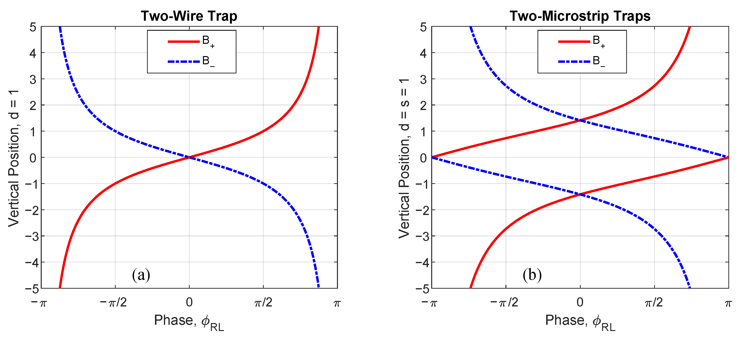
where the imaginary and real parts of the right-hand expression are identified as the trap coordinates , and both signs match to select for ± polarization. Solutions to are seen as negative complex conjugates of one another, tracing the same paths in opposite directions, with phase . The two-wire trap position in Equation (9) is plotted as “iso-r” curves for a cycle of phase delay at various values of current ratio in Figure 4. Paths that maintain phase (“iso-phase”) at and vary trace the dashed circle of radius d.
In the case of equal currents (), the trap is located at , with y controlled by phase as
We plot Equation (10) in Figure 5a, for each field across a cycle of phases. As phase shifts away from zero, the and minima move vertically in opposite directions away from . Perturbations are linear near (i.e., ), although this is not experimentally useful due to the chip’s surface. When currents are 180° out-of-phase (), the traps are asymptotically far away. The single trap returns to its original position after moving through a single cycle () of phase delay.
An instructive and useful special case is and , which yields for the field. This arrangement gives one polarization-specific trap in a useful location above the chip but leaves the other below the chip surface.
When , the trap crosses the x-axis outside of d for rather than asymptoting to as well as crossing the x-axis between the wires for . Plugging into Equation (9), we see the x-axis crossings occur at .
4.2. Two-Microstrip Trap
Adding a ground plane to the two-wire case moves the in-phase trap out of the chip substrate, usefully co-locating both minima outside of the chip. In this new geometry, the single wires become microstrip transmission lines for efficient microwave transmission, modeled using two mirror image currents, as seen in Figure 3 (right). Additionally, more traps are formed with, now, four complex currents (at and ), causing the field to cancel in two places for both and . We find the general expression for the location of the trap minima for both
where the left-hand side ± sign matches the leading right-hand side ± sign referring to , while the third ± sign inside the numerator gives both solutions per field polarization component. We plot this function in the same manner as before in Figure 4 (right). By counting 15° dots in Figure 4 or by counting curves for the case in Figure 5b, each phase now gives four trap locations simultaneously. Furthermore, the two traps of each polarization () travel in opposite directions with phase shifts. Each trap is located at over one cycle and at for another cycle, crossing over at and (for ). After a cycle of , the field returns to the same initial state, but if we label the two traps and track their motion, we see that each of the two traps moves to the other’s location in , returning to their initial locations over two full cycles, i.e., .
Extreme values of restrict paths to just around the wires, cycling each . As before in Figure 4 (right), black dashed curves mark the iso-phase for , now in two locations each. The dotted lines give the iso-phase circle marking , the in- and out-of-phase conditions, for .
Again, equal currents () restrict the trap location to , and the general vertical position as a function of phase difference is
where again the leading sign matches , and the inner sign gives two solutions. We plot these microstrip curves in Figure 5b, for .
Perturbing the phase around 0° with , one can separate opposite polarization traps vertically from co-location, but the trap frequencies differ and must be compensated for in an interferometer scheme. Additionally, this phase control scheme can co-locate one polarization’s minimum with a linear gradient or saddle-point regions from the opposite polarization’s field.
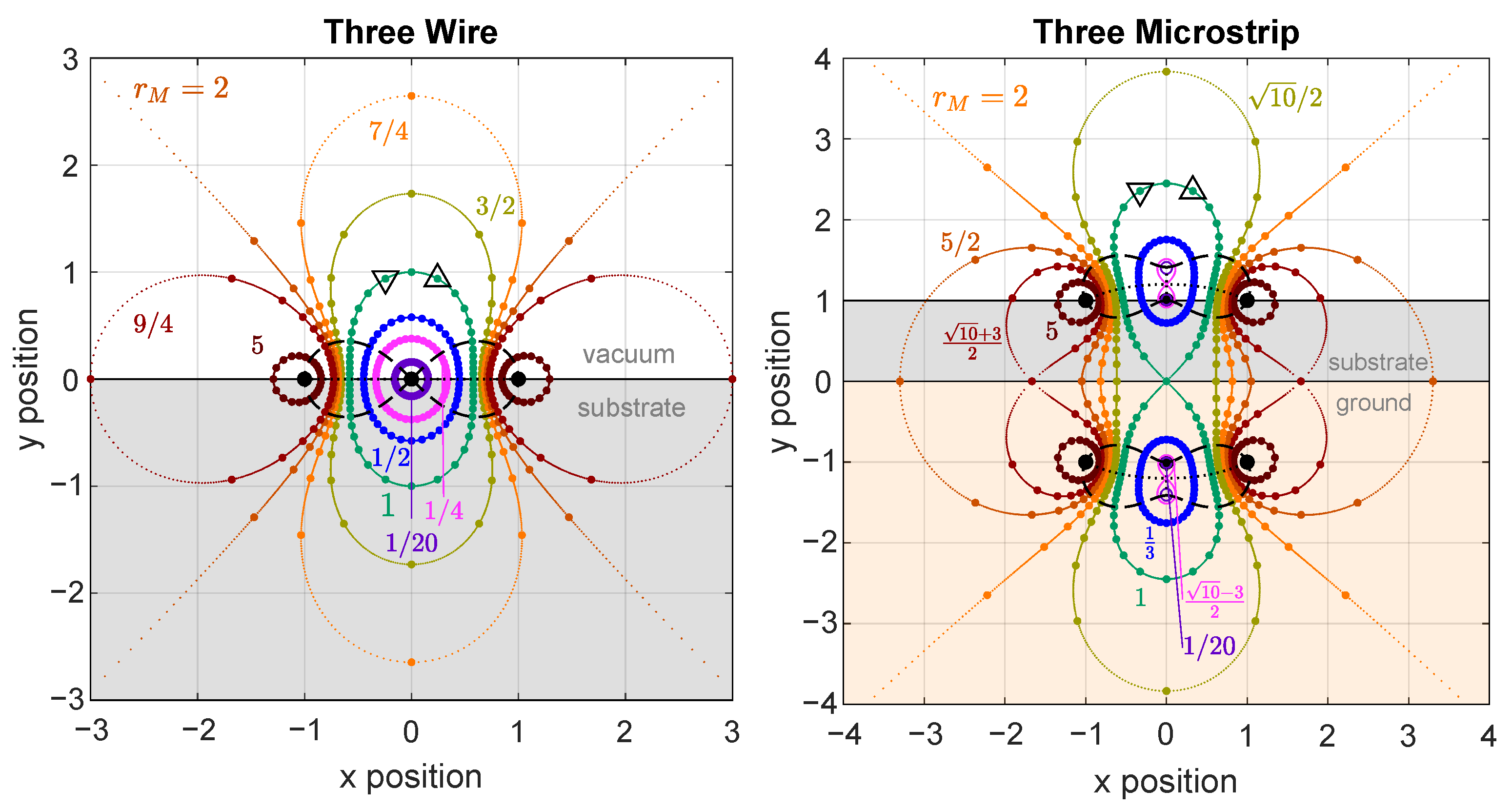
4.3. Three-Wire Trap
Considering the case of three currents (adding at to and at from Section 4.1, no images currents), we observe left–right separation of the spin polarization for phase shifts near 0°, fundamentally changing the behavior from the two-wire case. We restrict ourselves to the case of equal left and right currents in magnitude and phase, whereas we vary each of those parameters in the middle wire, with respect to the outer wires. We use , with , and . The positions of the zeroes of for three co-planar wires are given by
where each field (identified by the left-hand ± sign) has two solutions, distinguished by the ± sign on the right-hand side. The trap minima are plotted for various values for a cycle of , with in Figure 6. Again, as in the two-microstrip case in Section 4.2, the solutions in Equation (13) are periodic in . However, if atoms are in a given trap and the phase is varied continuously, then the atoms return to their original location after a cycle of , although the field looks identical over each cycle.
For , the trap positions form closed loops around the middle wire, convex for , growing to bulging bowling-pin shaped loops for , as shown in Figure 6 (left). At , i.e., the standard co-planar waveguide (CPW) configuration, a trap cannot form directly above the center trace (i.e., ). Furthermore, the trapping positions do not form a closed loop but instead demarcate diagonal asymptotes as , limiting the CPW as a useful ACZ trapping platform. When , the trap positions form two loops around the outer wires. As the phase is varied, the loops cross the x-axis once between the wires, and once outside, at .
An instructive case is , using , where a trap is formed at above the middle wire, and a quick mental sketch shows the vector-wise B-field cancellation. Perturbations around introduce imaginary components, shifting zeros left-and-right differentially (see △ and ▽ in Figure 6), making this scheme an interferometric spin separation candidate for use with a single frequency.
4.4. Three-Microstrip Trap
We convert the three-wire scheme from Section 4.3 to a three-microstrip layout by adding a ground plane and the three associated image currents. This arrangement of currents produces four zeroes for both and field polarizations. The general expression for the trap position () as a function of the center current’s relative amplitude and phase is given by
where the two ± signs on the right-hand side give four solutions and the left-hand side ± sign identifies the polarization. The four expressions are plotted in Figure 6 with the same formatting as Figure 4. The fields in Equation (14) still repeat when is advanced by , but similar to the two-microstrip and three-wire schemes, the phase must be advanced by multiples of for trapped atoms to return to their original locations. For different ranges of , it takes a , or advance in the phase to make a “total” cycle, depending on ’s magnitude, shown in Figure 6 (right). Crossovers between these regions of 4, 2, 1, 2, or 4 connected trap curves (shown by color or in Figure 6 (right)) are found to be simple expressions for , only for a simple case such as .
We can find topological boundary values of between the number of connected curves by locating curves that contain a “crossing” such as the curves in Figure 4, which can split into more curves, or merge into fewer curves with perturbations in . Mathematically, these values of mark the zeroes and poles under square roots in Equation (14), marking transitions between real and imaginary total values (trading x and y). Values of depend generally on the eccentricity of the design.
Similar to the three-wire trap, this microstrip arrangement (simulated in Section 5.2 for ) overlaps the traps for and then separates them horizontally as is shifted away from this value. Separation of the traps away from each other provides a potential beamsplitting mechanism for an atom interferometer (see also Section 6.1).
5. Simulations
We now move away from ideal 2-D trap models to discuss finite-sized, 3-D simulated versions of these microwave traps designed with 6.8 GHz as a target (87Rb hyperfine splitting) but usefully broadband as well. One approach to modeling chip performance is to use numerical electromagnetic simulation software to simulate the near field generated by sets of microstrips. We observe many features of microwave engineering that are not immediately evident from the pure current approach of Section 4, which we must take into account when designing these chip traps. Features (or hurdles) such as phase-dependent impedance, longitudinal propagation speeds, the skin and proximity effects, and surface roughness all add complexity to the situation. Using the results obtained from the simulation, we can reassess the theory to find out which approximations are justified. For instance, thin wires are not good approximations for broad chip traces when traps are only one or two trace widths away. Additionally, the AC skin effect’s adjustment of current density and phase within each trace [20] and the proximity effect between traces should be captured in proper near field calculations.
All of these effects can significantly impact the performance of the chip and trap properties, and therefore, simulations are necessary for determining their importance as well as for assessing chip designs. In this section, we present our simulations of two- and three-microstrip geometries and their expected performance. The simulations are conducted with the commercial software FEKO (Altair Inc., Troy, MI, USA) using the method of moments solutions. The simulations require a fairly high-density discretization (i.e., mesh) of the chip model traces in order to obtain reliable currents and fields (i.e., converged values). Additionally, the memory required to run simulations using the method of moments solutions increases with the square of the number of mesh elements. As such, these simulations must typically be run on a supercomputer cluster with terabyte-scale RAM memory.
5.1. Two Microstrip Traces
As shown in Section 4, the combination of magnetic near fields from multiple microstrip currents can result in a trapping potential for atoms in a given magnetic hyperfine state. This section examines an accurate 3-D model for a two-microstrip trap in order to determine the current distribution in the traces and the resulting trapping potential, as well as how these depend on phase.
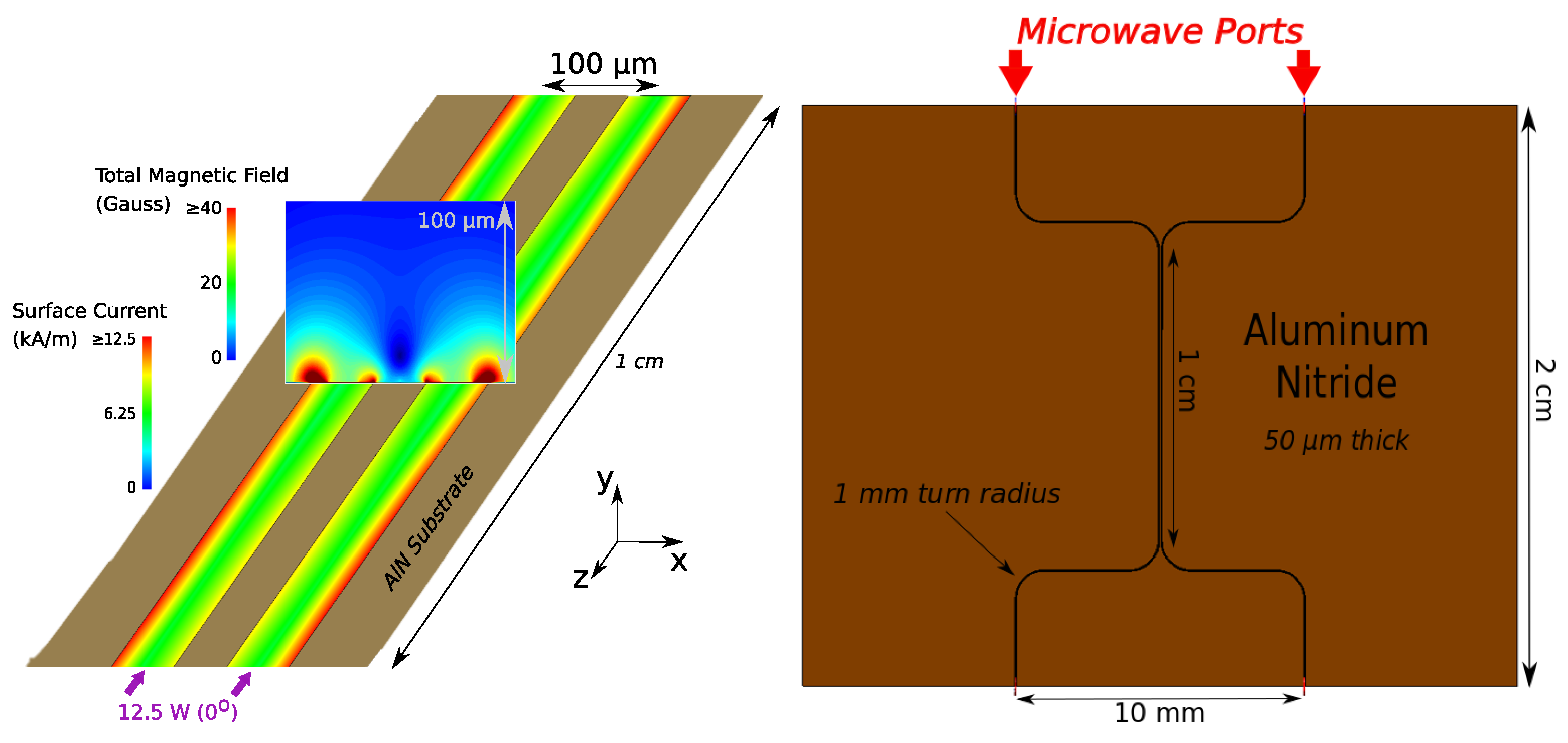
To overlap microwave near fields from multiple microstrips, we separate the traces by a distance of 100 μm center-to-center. Due to the 54 μm width of the microstrips, a scheme must be developed to transfer the microwaves from conventional connectorized cables (BNC and SMA) down to the micron scale while maintaining a 50 Ω impedance. Accommodating for such a device, we separate the input ports of the chip by 10 mm and similarly separate the output ports. To fulfill these requirements, we adopt the “double-s” configuration shown in Figure 7. Here, the chip is divided into two regions. The trapping region comprises two parallel 1 cm long microstrips spaced 100 μm center-to-center. The input (output) region consists of two microstrips that begin (end) at 10 mm separation, connected to two curved traces into (out of) the trapping region. In order to minimize the reflections for a curved microstrip, we employ a generous 1 mm turn radius, though the rule of thumb is to use a bend radius of at least three times the trace width [22].
5.1.1. Standard Configuration
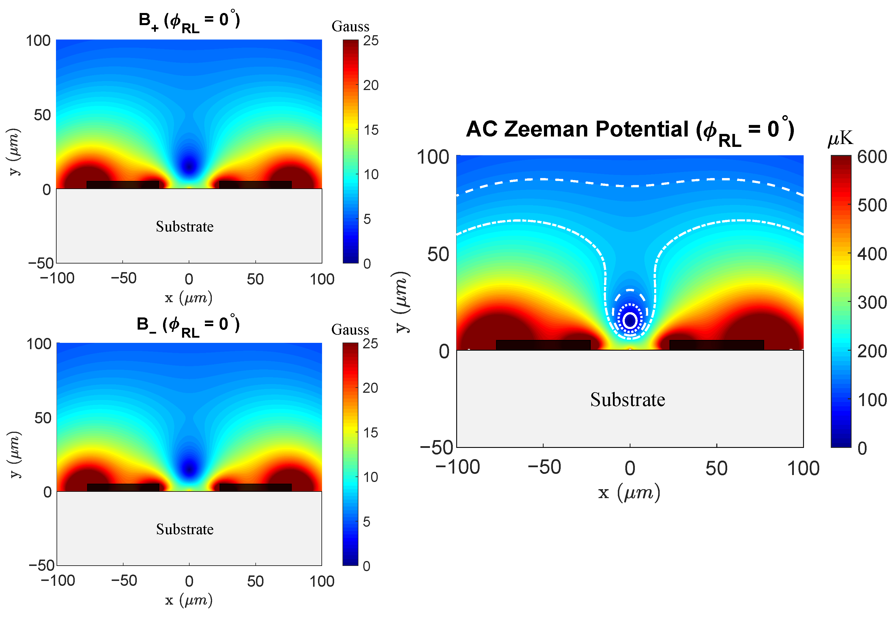
As outlined in Section 4.2, a benefit to using parallel microstrips is that the presence of the ground plane lifts the minimum of the combined magnetic field from the traces out of the plane of the chip. For currents in phase with one another, this results in co-located and traps. Using the model of Figure 7 (right), we direct 12.5 W into each input at 6.8 GHz with 50 Ω impedance and zero phase difference between the left and right ports. The resulting field components and corresponding ACZ potential for are shown in Figure 8. The substrate is shown in gray, and the black rectangles indicate the traces. Using Equation (5) for the magnetic hyperfine transition, we can convert the field into an ACZ potential. The conversion to μK uses , where is Boltzmann’s constant.
The simulation results in collocated traps above the microstrips, consistent with the simple theory of Section 4. However, as previously mentioned, the ideal theory does not account for the skin effect, which is present in our model at microwave frequencies. This effect can be seen in the current distribution of Figure 7, which shows higher current density near the edges of the traces. The proximity effect also has a strong effect on the current distribution and the resulting magnetic near field. As seen in Figure 7 and Figure 8, the in-phase currents in neighboring traces effectively repel each other, leading to larger current density and near field strength on the outer edges of the two traces. This effect is most easily visualized by looking at the current density in the traces for the in- and out-of-phase cases, shown in Figure 9. At equal phase, the coupling causes currents in each microstrip to be pushed away from each other, resulting in a larger current density on the outside edge of the microstrips. When the currents are set to be 180° out-of-phase, we observe the opposite effect and the currents are attracted to each other.
5.1.2. Phase Control
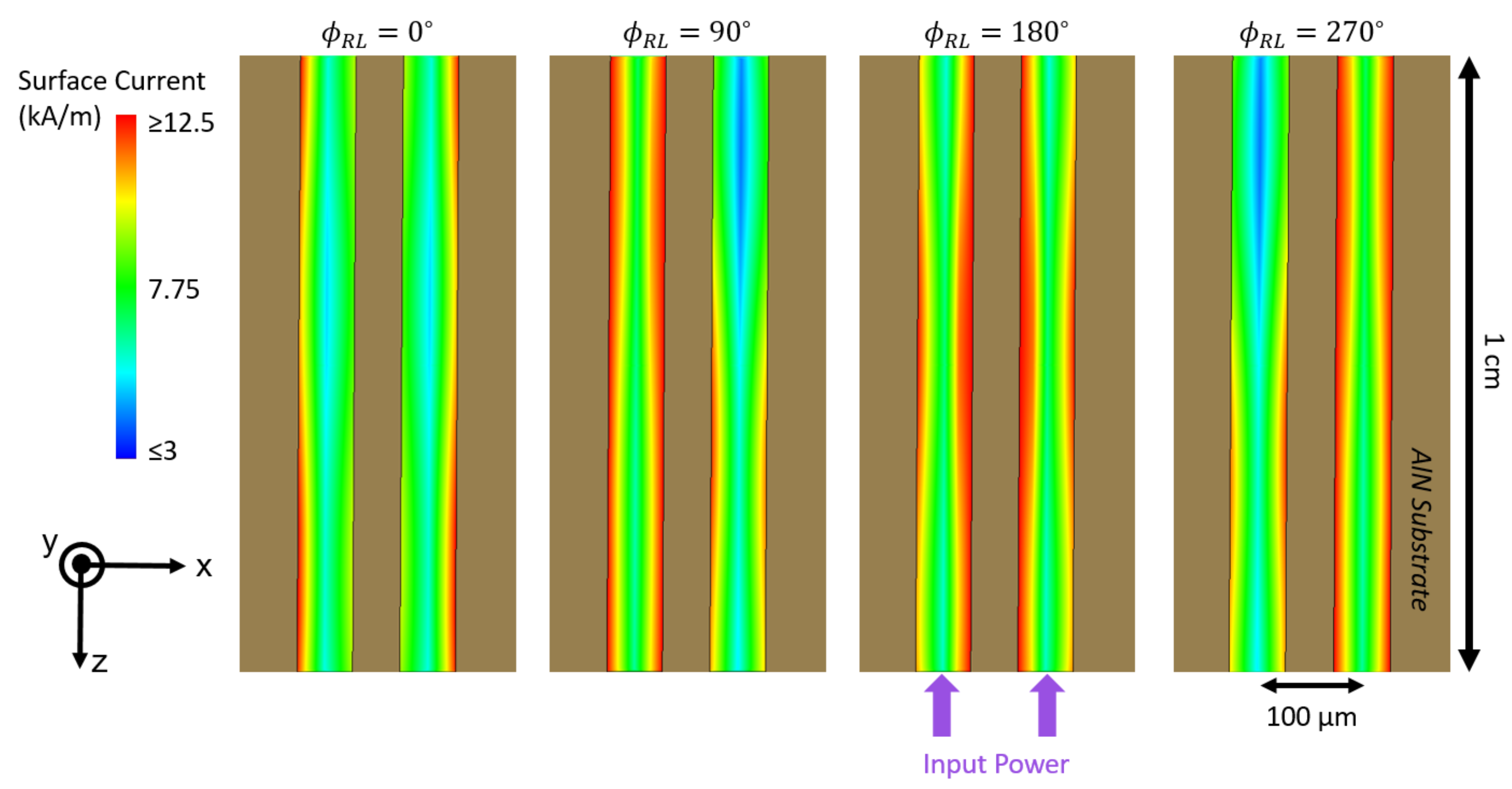
To show how controlling the relative phase of the inputs affects the trapping fields, we simulate the same two-microstrip model but now put the right trace ahead by 270° with respect to the left. The results of this simulation are shown in Figure 10.
An interesting result is that, unlike the in- and out-of-phase cases, the currents in the microstrips in the trapping region are not symmetric. Instead, we observe a current imbalance, resulting in the location of the trapping field shifting horizontally. We note that, for these non-symmetric cases, the trace that initially “lags behind” in phase at the inputs gains relative current magnitude and loses relative phase in the trapping region, shown in Figure 9. The symmetry in the currents can be viewed by considering the traveling modes of the parallel microstrip configuration. In this system, the eigennmodes are given by the currents being completely in- or out-of-phase (0° and 180°) [18,19]. In these cases, we expect the currents in the microstrips to be well-behaved, modulo skin and proximity effects. For other phase differences, the traveling mode is a linear superposition of the eigenmodes, resulting in possible non-symmetry between the traces. The proximity of the microstrips may also cause the current to move between the traces via a displacement current induced by coupling. In designing a microwave atom chip, one must be aware of such effects on the microstrip’s current and phase in the trapping region. Possible schemes to minimize these effects are to increase the trace separation in the trapping region and to adjust the input power and phases to account for the current differential.
5.2. Three-Microstrip Traces
Similar to the two-microstrip model, the three-microstrip design consists of two “s-curves” with an additional straight trace running between them (Figure 11). The addition of a third microstrip trace offers a couple of avenues for interferometry. As demonstrated in Section 4.4, altering the phase of the center trace relative to the outer traces spatially separates the trap minima horizontally along the x-direction above the chip surface. This single-frequency trap splitting has been observed in simulation; however, it is not the primary means of interferometry intended with this chip. Using multiple frequencies, one could realize overlapping independent spin-specific traps that could subsequently be translated horizontally onto microwave lattices generated on each of the outer traces, as described in Section 6.
To achieve the 180° phase difference for the center trace current in the central section of the chip (see Section 4.4), we note that the different travel distances of the microwaves for the center and side traces must be accounted for (in units of wavelength). For instance, at 6.8 GHz, a trap is formed for a center input phase of 80° (Figure 11), while at 10 GHz, the input phase is 5°. Additionally, an unintentional lattice is formed on the center microstrip due to possible couplings or reflections, affecting how the current propagates along the center trace.
Additionally, the skin and proximity effects described in previous sections are present. Examining the two outer traces in Figure 11, the current density is seemingly larger on the inner part of the trace than the outer trace, corresponding to a deeper red coloring. This behavior agrees with what we encountered in Section 5.1 from the proximity effect. Since in this region the outer currents are roughly 180° out of phase with the center, the currents in the two outer traces tend to be attracted towards the inner trace.
By lowering the power and current in the center trace, the trap is pulled closer to the chip while also reducing crosstalk to outer traces. For 8 W of input on the side microstrips and 0.5 W on the center trace, as shown in Figure 11, the trap is located 93 μm above the chip and has a depth of ∼15 μK.
6. Microwave Lattice
A microwave lattice, i.e., standing wave, can provide a flexible mechanism for both axial confinement and axial positioning along the length of a microstrip trace. If microwaves of equal amplitude are directed from both ends of a trace, then a magnetic standing wave is created as well as an electric standing wave 90° out of phase with the former. The effective index of refraction for a TEM wave in our 50 Ω microstrip with an AlN substrate is ∼2.5, which results in a wavelength of = 1.8 cm at 6.8 GHz ( = 4.4 cm in vacuum) and magnetic minima every 0.9 cm. The lattice can be translated axially along the microstrip by adjusting the relative phase between the two counter-propagating waves.
The three-microstrip trapping potential in Section 5.2 provides confinement in the -plane transverse to the microstrips but not longitudinally along the z-axis. A microwave lattice applied to the center microstrip at a frequency offset from the transverse trapping microwave fields provides axial confinement. As long as is much faster than the mechanical response of an atom (e.g., = 1 MHz versus = 0.1–1 kHz), the atoms only respond to the average microwave field magnitude at a given frequency, and thus, the total potential is just the sum of the lattice and transverse potentials.
If spin-independent axial confinement is needed or if a different spatial period is required, then the lattice can be operated away from the hyperfine transition used for the transverse potentials via the AC Stark potential of the electric standing wave. For microwaves, the AC Stark effect is in the quasi-static regime, so the Stark potential is well approximated by the DC Stark energy shift , where is the DC polarizability of the atom and is the rms magnitude of the microwave electric field. While the AC Stark potential is typically much weaker than the ACZ energy, in the very far detuned limit, it dominates. Furthermore, at high power or very close to a microstrip trace, the AC Stark potential can become sufficiently strong to provide useful axial confinement at the location of the lattice electric field maximum, which is also the magnetic field minimum (zero).
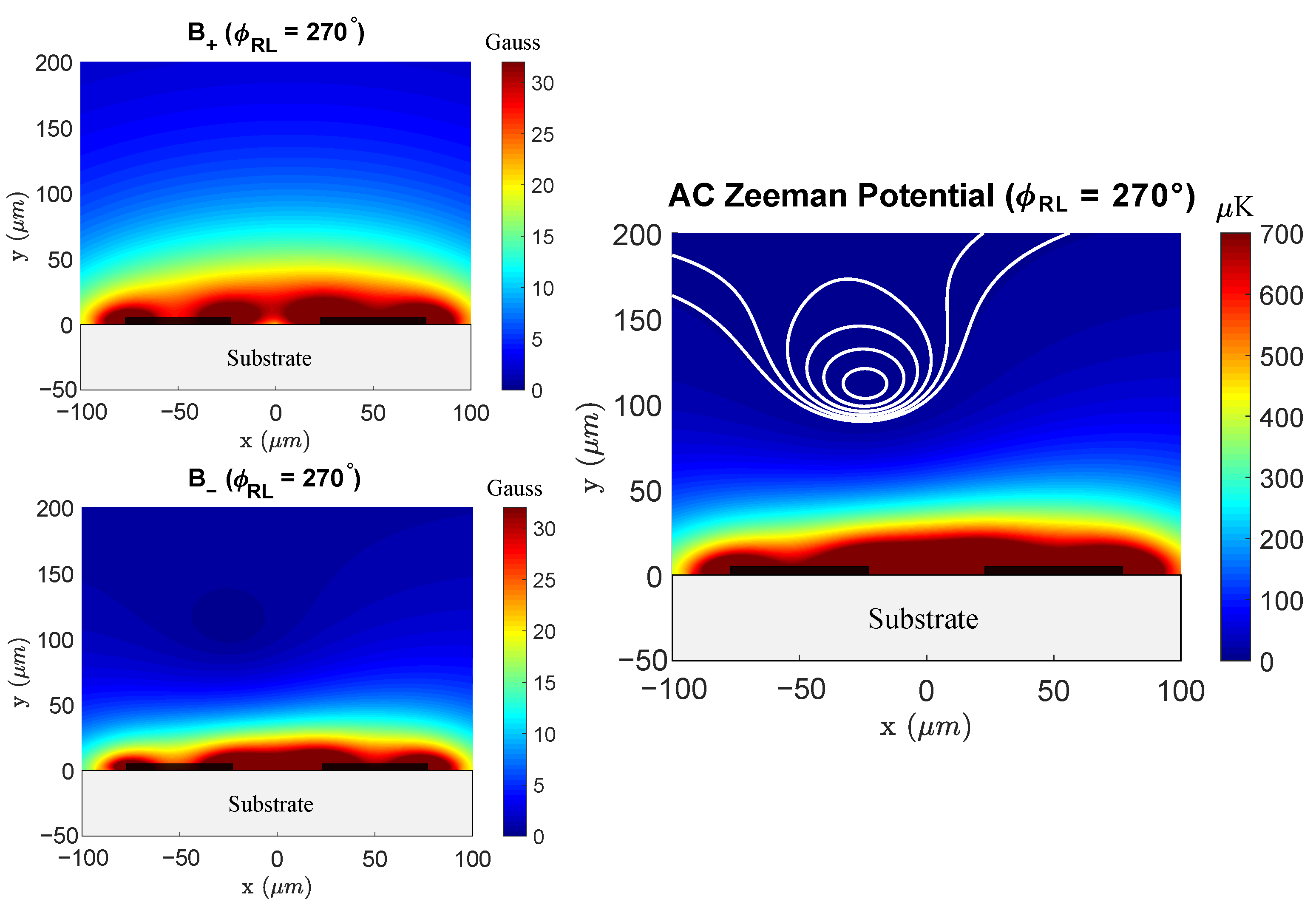
Figure 12a shows the ACZ and AC Stark potentials of a microwave lattice produced by a standing wave current in a single microstrip (same design as in Figure 2), generated by two counter-propagating 12.5 W traveling TEM waves at 6.8 GHz directed from either end of the microstrip. The microwave frequency has a detuning of MHz on the
87Rb transition, and the lattice potential is evaluated 100 μm above the microstrip. In this example, the axial confinement is 30.1 Hz and 2.8 Hz for the ACZ and AC Stark potentials, respectively, thus showing that the lattice can provide adjustable and re-positionable axial confinement for a transverse ACZ trap.
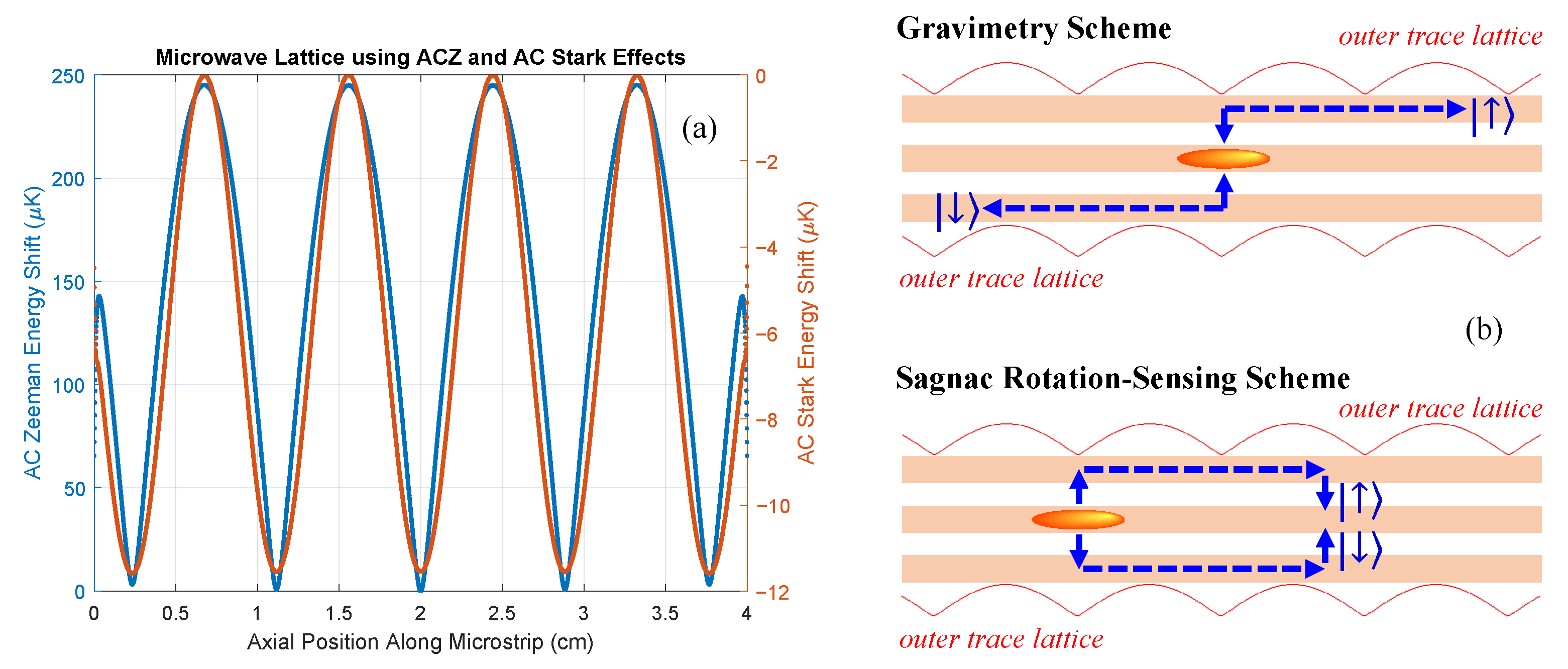
6.1. Axial Interferometry
Microwave lattices enable potentially large interferometer arm separations on the cm scale. Spin-specific transverse trap positioning can be used to beamsplit and separate spin states towards the outer traces of the three-microstrip geometry, while microwave lattices on these outer traces can then be used to translate the spin states axially for cm-scale interferometer arm separations. Microwave lattices on the outer traces can use an ACZ potential (spin-dependent) or an AC Stark potential (spin-independent). In the latter case, the lattice can be operated at a much higher microwave frequency for tighter axial confinement. As shown in Figure 12b, this interferometer architecture can operate in a gravimeter configuration (outer lattices translate in opposite directions for a large arm separation) or in a Sagnac configuration (outer lattices translate in the same direction for a large enclosed area).
While each lattice is localized on an outer trace, there can be residual “crosstalk”, where the lattice potential from one trace perturbs the trapping potential for spin states on the other trace. This crosstalk between the lattices on the outer traces can be minimized by applying lattice currents (at a given microwave frequency) to multiple microstrips with the appropriate phases and amplitudes to further suppress the unwanted lattice at a spin state’s location, i.e., make a “trap” or microwave lattice field minimum (zero) at its location.
6.2. Interferometer Stability
The viability of the spin-dependent interferometry approach depends on the stability of the interferometric phase with respect to imperfections and noise in the system parameters as well as to external magnetic field noise. We identify three main decoherence and de-phasing mechanisms: (1) Asymmetry of the two spin-dependent traps that constitute the interferometer arms, (2) gravimetric sensitivity of arm displacements to microwave trapping parameter fluctuations, and (3) differential DC Zeeman shifts between the two spin states.
6.2.1. Asymmetry Decoherence
Any asymmetry in the trap frequency of the harmonic traps for the two spin states lead to decoherence, since the spin states then have slightly different trap state energies and thus dephase over time. This decoherence mechanism has been studied both theoretically [4,23] and experimentally [24]: the coherence time is given by , where is the trap frequency, is the trap frequency asymmetry, and T is the temperature of the atoms ( is Boltzmann’s constant). While the symmetry of the traps can be enforced by the careful adjustments of trap parameters over the course in the interferometry process, uncontrolled deviations in the parameters ultimately lead to asymmetry fluctuations in the two traps. In a microwave ACZ trap, deviations in the trap frequency are directly related to the microwave power fluctuations (via the Rabi frequency Ω) and the microwave frequency stability (via the detuning ).
Table 1 shows the tolerance on trap system parameters to ensure a coherence time of s. We use a target coherence time s, since such a time is useful for competitive atom interferometry measurements [25], and such a time has been demonstrated in atom chip-based Ramsey interferometers [26,27]. The power and frequency tolerance requirements are derived from the trap frequency asymmetry requirement. A power stability of requires active microwave amplitude stabilization. The microwave frequency stability of is based on a detuning of 1 MHz and is well within the stability of commercial oscillators referenced to a high-quality clock.
6.2.2. Gravimetric Dephasing
If the two traps of the interferometer experience a differential vertical position fluctuation, i.e., along the local direction of gravity, then a corresponding gravimetric fluctuation in the interferometer phase accrues. This gravimetric contribution to the interferometer phase is given by , where m is the mass of the atom, g is the local acceleration due to gravity, t is the interrogation time, and is the vertical position fluctuation. In a three-trace trap, the trap position is controlled by the microwave power (y-axis), the phase of the transverse trapping microwave currents (x-axis), and the microwave lattice phase (z-axis).
Table 2 shows the required stability on the vertical position and the corresponding stability on the microwave parameters to ensure an interferometer phase variation for an interrogation time of s (for an ultracold rubidium-based interferometer). The stability requirements on the microwave parameters (power and phase) necessitates their active stabilization. Shortening the interrogation to ms relaxes the stability requirements by a factor of 10.
6.2.3. Differential Zeeman Shifts
Technical and environmental magnetic field noise generate spin-dependent DC Zeeman energy shifts in the two spin states used in the interferometer. The resulting energy fluctuations quickly de-phase the interferometer signal, so a mitigation strategy is needed. If the spin state pair have a “magic” magnetic field, then at this field the differential Zeeman shift between the two spin states is zero and thus immune to magnetic field noise (to first order). Table A3 in Appendix B shows the low-field magic magnetic fields for rubidium and potassium isotopes of interest. Notably, the use of the 3.23 G magic magnetic field for the , and spin states of 87Rb has resulted in a coherence time of about 1 s for a Ramsey interferometer based on atoms in a micromagnetic chip trap [26] and in a laser dipole trap [27].
7. Conclusions
In summary, we presented several microwave traps targeted toward use in trapped atom interferometry based on an atom chip with microstrip transmission lines. Utilizing the near field generated by sets of two or three microstrips, we can make use of the ACZ effect to produce a trap for ultracold atoms in a specific hyperfine spin state. This spin-specific trapping scheme offers experimental control variables not currently part of the ultracold atom chip toolbox. detuning of the microwave magnetic field affects the shape of the trap, changing from linear near resonance to more quadratic as detuning increases. Additionally, adjusting the phase of the field-generating microwave currents allows for the targeting of specific hyperfine magnetic states using circularly polarized fields.
While the microstrip geometries described in this paper generate near field traps from microwaves, we have not addressed how to couple microwaves into and out of the chip. An important engineering task is to efficiently transfer (i.e., “focus”) microwaves in coaxial cables with mm-scale TEM field modes into the 54 μm-wide microstrips. Areas of current interest are the design and simulation of tapered connectors, tapered coplanar waveguides, and micro-coaxial cables [28].
While this paper focused on microwave ACZ traps geared towards interferometry, such spin-specific trapping has other useful applications. For example, in 1D many-body systems, the collective eigenmodes manifest themselves as pure spin or charge (“charge” here refers to density) wave packets that propagate at different velocities [29]. By overlapping two 1D gases comprising different spin states, a spin-specific potential could be used to control interactions and the resulting spin-charge separation [30]. The microwave ACZ traps could also be used to realize spin-based quantum gates, in which entanglement between internal atomic spin states can be mediated by the spin-specific ACZ potential, as is pursued in the ion quantum computing community [31,32,33,34].
Finally, we note in closing that atom chips based on ACZ near field traps are expected to benefit from the suppression of potential roughness. Resulting from the transfer of chip wire defects into the trapping potential, this roughness is a frequent concern when using atom chips [35]. Fortunately, current theoretical work indicates that such roughness is expected to be significantly suppressed in RF and microwave ACZ chip traps [36,37,38].
Author Contributions
Conceptualization, S.A.; methodology, W.M., A.P.R., S.D. and S.A.; software, W.M., A.P.R., S.D. and S.A.; validation, W.M., A.P.R., S.D. and S.A.; formal analysis, W.M., A.P.R., S.D. and S.A.; investigation, W.M., A.P.R., S.D. and S.A.; resources, S.A.; writing—original draft preparation, W.M., A.P.R., S.D. and S.A.; writing—review and editing, W.M., A.P.R., S.D. and S.A.; visualization, W.M., A.P.R. and S.A.; supervision, S.A.; project administration, S.A.; funding acquisition, S.A. All authors have read and agreed to the published version of the manuscript.
Funding
This research was funded by the National Science Foundation grant number 1806558, by the Defense Threat Reduction Agency grant number HDTRA1-19-1-0027, and by the College of William & Mary.
Institutional Review Board Statement
Not applicable.
Informed Consent Statement
Not applicable.
Data Availability Statement
The data presented in this study are available from the corresponding author upon request.
Acknowledgments
The authors acknowledge William & Mary Research Computing for providing the computational resources and/or technical support that have contributed to the results reported within this paper. https://www.wm.edu/it/rc.
Conflicts of Interest
The authors declare no conflict of interest.
Abbreviations
The following abbreviations are used in this manuscript:
| AC | alternating current |
| DC | direct current |
| RF | radio frequency |
| microwave | |
| ACZ | AC Zeeman |
| TEM | transverse electro-magnetic |
| hfs | hyperfine state |
Appendix A. Matrix Elements in the Rabi Frequency
In the low-field limit, , where is the ground hyperfine splitting, and are “good” quantum numbers, and are eigenstates of the atomic Hamiltonian. We calculate the Clebsch–Gordan coefficients for the hyperfine states for the inter-manifold microwave transitions as
For the low-frequency intra-manifold transitions, we have
where ( for ). These elements identify the transitions allowed with a Kronecker delta, give the relative transition probability values, and select a single polarization field per transition. We list explicit values for the inter-manifold values in Table A1 and for the intra-manifold values in Table A2.
As an example, consider the inter-manifold transition () in the presence of a microwave magnetic field with G, where the time dependence is contained in a complex exponential (see Section 4). From the -function in the above equations for the inter-manifold transitions, the only non-vanishing contribution in Equation (3) contains . The magnitude of the Rabi frequency is then . Using the provided tables (Table A1), we see that for this transition. Therefore, MHz.

Table A1.
Clebsch–Gordan coefficients (factor of ħ/4 pulled out) used to to determine the Rabi frequency for the inter-manifold transitions (). Note that the coefficients have a factor of 2 included to match the form of the Rabi frequency given in Equation (3).
Table A1.
Clebsch–Gordan coefficients (factor of ħ/4 pulled out) used to to determine the Rabi frequency for the inter-manifold transitions (). Note that the coefficients have a factor of 2 included to match the form of the Rabi frequency given in Equation (3).
| m | m | ||||||
|---|---|---|---|---|---|---|---|
| +1 | 2 | 2 | 1 | 1 | 0 | 0 | |
| 2 | 1 | 1 | 0 | 0 | 0 | ||
| 2 | 0 | 1 | −1 | 0 | 0 | ||
| −1 | 2 | 0 | 1 | 1 | 0 | 0 | |
| 2 | −1 | 1 | 0 | 0 | 0 | ||
| 2 | −2 | 1 | −1 | 0 | 0 | ||
| 0 | 2 | 1 | 1 | 1 | 0 | 0 | |
| 2 | 0 | 1 | 0 | 0 | 0 | −4 | |
| 2 | −1 | 1 | −1 | 0 | 0 |
Table A2.
Clebsch–Gordan coefficients (factor of pulled out) used to determine the Rabi frequency for the intra-manifold transitions (). Note that the coefficients have a factor of 2 included to match the form of the Rabi frequency given in Equation (3).
Table A2.
Clebsch–Gordan coefficients (factor of pulled out) used to determine the Rabi frequency for the intra-manifold transitions (). Note that the coefficients have a factor of 2 included to match the form of the Rabi frequency given in Equation (3).
| m | F | m | F | m | ||||||||
|---|---|---|---|---|---|---|---|---|---|---|---|---|
| +1 | 2 | 2 | 1 | 2 | 0 | 0 | 1 | 1 | 0 | 0 | 0 | |
| 2 | 1 | 0 | 0 | 0 | ||||||||
| 2 | 0 | −1 | 0 | 0 | 1 | 0 | −1 | 0 | 0 | |||
| 2 | −1 | −2 | 2 | 0 | 0 | |||||||
| −1 | 2 | 1 | 2 | 0 | 2 | 0 | 1 | 0 | 1 | 0 | 0 | |
| 2 | 0 | 1 | 0 | 0 | ||||||||
| 2 | −1 | 0 | 0 | 0 | 1 | −1 | 0 | 0 | 0 | |||
| 2 | −2 | −1 | 0 | 2 | 0 | |||||||
| 0 | 2 | 2 | 2 | 0 | 0 | 4 | 1 | 1 | 1 | 0 | 0 | −2 |
| 2 | 1 | 1 | 0 | 0 | 2 | |||||||
| 2 | 0 | 0 | 0 | 0 | 0 | 1 | 0 | 0 | 0 | 0 | 0 | |
| 2 | −1 | −1 | 0 | 0 | −2 | 1 | −1 | −1 | 0 | 0 | 2 | |
| 2 | −2 | −2 | 0 | 0 | −4 |
Additionally, we note that while both and can have nonzero values for RF transitions within in each manifold on paper, in practice, the level structure of each hyperfine manifold determines its circular polarization with the level’s gyromagnetic ratio . In the case of 87Rb, the (1) manifold has (), forcing any addition of photon energy to alter () via solely () transitions [12]. Additionally, the intra-manifold self-term can be identified as the DC Zeeman value.
Appendix B. Rubidium vs. Potassium
When using atoms as sensitive clocks or matter-wave interferometers, reducing the sensitivity to environmental magnetic field fluctuations and noise is generally necessary. Given the ACZ effect’s ability to utilize any spin state, we can target so-called “clock states” that have identical linear DC Zeeman shifting, accounting for higher-order effects, turning noise in the magnetic field into a common-mode noise, and leaving a second-order magnetic dependence instead. The classic example is between 87Rb’s and at 3.23 Gauss, but this is a two-photon transition, where one photon is nearly 6.8 GHz.
Isotopes of potassium, both fermions and bosons, have hyperfine splittings much lower, around 250 MHz and 1.3 GHz. We list some available “magic” magnetic fields that produce good clock states in Rb and K in Table A3. Operating at lower frequency relaxes some chip design constraints needed for microwave frequencies as well as allows for easier phase control and more precise signal generation. Additionally, potassium benefits from improved spin-specificity because the magic magnetic fields are typically an order of magnitude larger than in 87Rb so neighboring (unwanted) transitions are also an order of magnitude further off resonance.
Table A3.
Low-field “magic” magnetic fields for 87Rb, 41K, and 40K. All values are computed. “Zeeman splittings” refers to the energy splittings with states neighboring the “state pair”.
Table A3.
Low-field “magic” magnetic fields for 87Rb, 41K, and 40K. All values are computed. “Zeeman splittings” refers to the energy splittings with states neighboring the “state pair”.
| Isotope | “Magic” Field (G) | State Pair Basis | Energy (MHz) | Zeeman Splittings (MHz) |
|---|---|---|---|---|
| 87Rb | 3.23 | 6834.7 | ∼2 | |
| 41K | 24.47 | 245.4 | 15–21 | |
| 24.36 | 245.3 | 15–18 | ||
| 45.36 | 219.9 | 32–47 | ||
| 40K | 0.72 | 1285.0 | ∼0.2 | |
| 50.96 | 1277.8 | ∼16 | ||
| 53.56 | 1277.4 | 16–18 | ||
| 53.74 | 1277.4 | 16–18 | ||
| 63.55 | 1275.9 | 19–22 | ||
| 63.95 | 1275.8 | 19–22 |
References
- Moan, E.; Horne, R.; Arpornthip, T.; Luo, Z.; Fallon, A.; Berl, S.; Sackett, C. Quantum rotation sensing with dual Sagnac interferometers in an atom-optical waveguide. Phys. Rev. Lett. 2020, 124, 120403. [Google Scholar] [CrossRef] [Green Version]
- Gibble, K. Decoherence and collisional frequency shifts of trapped bosons and fermions. Phys. Rev. Lett. 2009, 103, 113202. [Google Scholar] [CrossRef]
- Hazlett, E.L.; Zhang, Y.; Stites, R.W.; Gibble, K.; O’Hara, K.M. S-Wave collisional frequency shift of a fermion clock. Phys. Rev. Lett. 2013, 110, 160801. [Google Scholar] [CrossRef] [Green Version]
- Ammar, M.; Dupont-Nivet, M.; Huet, L.; Pocholle, J.P.; Rosenbusch, P.; Bouchoule, I.; Westbrook, C.I.; Estève, J.; Reichel, J.; Guerlin, C.; et al. Symmetric microwave potentials for interferometry with thermal atoms on a chip. Phys. Rev. A 2015, 91, 053623. [Google Scholar] [CrossRef] [Green Version]
- Dupont-Nivet, M.; Westbrook, C.I.; Schwartz, S. Effect of trap symmetry and atom-atom interactions on a trapped-atom interferometer with internal state labeling. Phys. Rev. A 2021, 103, 023321. [Google Scholar] [CrossRef]
- LeBlanc, L.; Thywissen, J. Species-specific optical lattices. Phys. Rev. A 2007, 75, 053612. [Google Scholar] [CrossRef] [Green Version]
- Fancher, C.; Pyle, A.; Rotunno, A.; Aubin, S. Microwave ac Zeeman force for ultracold atoms. Phys. Rev. A 2018, 97, 043430. [Google Scholar] [CrossRef] [Green Version]
- Dalibard, J.; Cohen-Tannoudji, C. Dressed-atom approach to atomic motion in laser light: The dipole force revisited. JOSA B 1985, 2, 1707–1720. [Google Scholar] [CrossRef] [Green Version]
- Agosta, C.C.; Silvera, I.F.; Stoof, H.T.C.; Verhaar, B.J. Trapping of neutral atoms with resonant microwave radiation. Phys. Rev. Lett. 1989, 62, 2361. [Google Scholar] [CrossRef] [PubMed] [Green Version]
- Tiesinga, E.; Mohr, P.J.; Newell, D.B.; Taylor, B.N. CODATA recommended values of the fundamental physical constants: 2018. Rev. Mod. Phys. 2021, 93, 025010. [Google Scholar] [CrossRef]
- Metcalf, H.J.; van der Straten, P. Laser Cooling and Trapping; Springer: Berlin/Heidelberg, Germany, 1999. [Google Scholar]
- Perrin, H.; Garraway, B.M. Trapping atoms with radio frequency adiabatic potentials. Adv. At. Mol. Opt. Phys. 2017, 66, 181–262. [Google Scholar]
- Schumm, T.; Hofferberth, S.; Andersson, L.M.; Wildermuth, S.; Groth, S.; Bar-Joseph, I.; Schmiedmayer, J.; Krüger, P. Matter-wave interferometry in a double well on an atom chip. Nat. Phys. 2005, 1, 57–62. [Google Scholar] [CrossRef] [Green Version]
- Grieg, D.; Engelmann, H. Microstrip-A new transmission technique for the kilomegacycle range. Proc. IRE 1952, 40, 1644–1650. [Google Scholar] [CrossRef]
- Böhi, P.; Riedel, M.F.; Hoffrogge, J.; Reichel, J.; Hänsch, T.W.; Treutlein, P. Coherent manipulation of Bose–Einstein condensates with state-dependent microwave potentials on an atom chip. Nat. Phys. 2009, 5, 592–597. [Google Scholar] [CrossRef]
- Lowry, B.; Wyllie, R.; Chapman, M.; Herold, C. Characterization of an Atom Chip with Integrated Coplanar Waveguides. In Proceedings of the APS Division of Atomic, Molecular and Optical Physics Meeting Abstracts, Ft. Lauderdale, FL, USA, 28 May–1 June 2018; Volume 63. [Google Scholar]
- Lu, Z.; Murakowski, J.A.; Schuetz, C.A.; Shi, S.; Schneider, G.J.; Samluk, J.P.; Prather, D.W. Perfect lens makes a perfect trap. Opt. Express 2006, 14, 2228–2235. [Google Scholar] [CrossRef] [PubMed]
- Orfanidis, S.J. Electromagnetic Waves and Antennas; Rutgers University: New Brunswick, NJ, USA, 2002. [Google Scholar]
- Collin, R.E. Foundations for Microwave Engineering; John Wiley & Sons: Hoboken, NJ, USA, 2007. [Google Scholar]
- Blackwell, A.E.; Rotunno, A.P.; Aubin, S. Demonstration of the lateral AC skin effect using a pickup coil. Am. J. Phys. 2020, 88, 676–684. [Google Scholar] [CrossRef]
- Rotunno, A.P.; Du, S.; Miyahira, W.; Aubin, S. Radiofrequency AC Zeeman Trapping for Ultracold Atoms. Manuscript in preparation.
- Lee, T.H.; Lee, T.H. Planar Microwave Engineering: A Practical Guide to Theory, Measurement, and Circuits; Cambridge University Press: Cambridge, UK, 2004; Volume 1. [Google Scholar]
- Dupont-Nivet, M.; Westbrook, C.; Schwartz, S. Contrast and phase-shift of a trapped atom interferometer using a thermal ensemble with internal state labelling. New J. Phys. 2016, 18, 113012. [Google Scholar] [CrossRef] [Green Version]
- Dupont-Nivet, M.; Demur, R.; Westbrook, C.I.; Schwartz, S. Experimental study of the role of trap symmetry in an atom-chip interferometer above the Bose–Einstein condensation threshold. New J. Phys. 2018, 20, 043051. [Google Scholar] [CrossRef]
- Dickerson, S.M.; Hogan, J.M.; Sugarbaker, A.; Johnson, D.M.; Kasevich, M.A. Multiaxis inertial sensing with long-time point source atom interferometry. Phys. Rev. Lett. 2013, 111, 083001. [Google Scholar] [CrossRef] [Green Version]
- Treutlein, P.; Hommelhoff, P.; Steinmetz, T.; Hänsch, T.W.; Reichel, J. Coherence in microchip traps. Phys. Rev. Lett. 2004, 92, 203005. [Google Scholar] [CrossRef] [PubMed] [Green Version]
- Du, S. AC & DC Zeeman Interferometric Sensing with Ultracold Trapped Atoms on Chip. Ph.D. Thesis, College of William and Mary, Williamsburg, VA, USA, 2021. [Google Scholar]
- Torres, D.; Kopa, A.; Meinhold, M.; Lewis, P.; Delisio, J.; Gray, C. Microcoaxial Interconnects for Signals, Bias, and Supply of MMICs. In Proceedings of the 2019 IEEE MTT-S International Microwave Symposium (IMS), Boston, MA, USA, 2–7 June 2019; pp. 1046–1049. [Google Scholar]
- Recati, A.; Fedichev, P.; Zwerger, W.; Zoller, P. Spin-charge separation in ultracold quantum gases. Phys. Rev. Lett. 2003, 90, 020401. [Google Scholar] [CrossRef] [PubMed] [Green Version]
- Spielman, I.; National Institute of Standards and Technology, Gaithersburg, MD, USA. Personal communication, 2014.
- Ospelkaus, C.; Warring, U.; Colombe, Y.; Brown, K.; Amini, J.; Leibfried, D.; Wineland, D.J. Microwave quantum logic gates for trapped ions. Nature 2011, 476, 181–184. [Google Scholar] [CrossRef] [PubMed] [Green Version]
- Harty, T.; Allcock, D.; Ballance, C.J.; Guidoni, L.; Janacek, H.; Linke, N.; Stacey, D.; Lucas, D. High-fidelity preparation, gates, memory, and readout of a trapped-ion quantum bit. Phys. Rev. Lett. 2014, 113, 220501. [Google Scholar] [CrossRef] [Green Version]
- Hahn, H.; Zarantonello, G.; Bautista-Salvador, A.; Wahnschaffe, M.; Kohnen, M.; Schoebel, J.; Schmidt, P.; Ospelkaus, C. Multilayer ion trap with three-dimensional microwave circuitry for scalable quantum logic applications. Appl. Phys. B 2019, 125, 1–10. [Google Scholar] [CrossRef] [Green Version]
- Romaszko, Z.D.; Hong, S.; Siegele, M.; Puddy, R.K.; Lebrun-Gallagher, F.R.; Weidt, S.; Hensinger, W.K. Engineering of microfabricated ion traps and integration of advanced on-chip features. Nat. Rev. Phys. 2020, 2, 285–299. [Google Scholar] [CrossRef]
- Krüger, P.; Andersson, L.M.; Wildermuth, S.; Hofferberth, S.; Haller, E.; Aigner, S.; Groth, S.; Bar-Joseph, I.; Schmiedmayer, J. Potential roughness near lithographically fabricated atom chips. Phys. Rev. A 2007, 76, 063621. [Google Scholar] [CrossRef] [Green Version]
- Du, S.; Rotunno, A.; Sullivan, K.; Aubin, S. Potential roughness suppression in microwave chip traps. In Proceedings of the APS Division of Atomic, Molecular and Optical Physics Meeting Abstracts, Milwaukee, WI, USA, 27–31 May 2019; Volume 63. [Google Scholar]
- Ziltz, A.R. Ultracold Rubidium and Potassium System for Atom Chip-Based Microwave and RF Potentials. Ph.D. Thesis, College of William and Mary, Williamsburg, VA, USA, 2015. [Google Scholar]
- Du, S.; Ziltz, A.R.; Aubin, S. Suppression of Potential Roughness in Atom Chip AC Zeeman Traps. Phys. Rev. A 2021. submitted. [Google Scholar]
Figure 1.
Two-level atom in the presence of a microwave magnetic field. (a) The dressed atom energies (red and blue curves) given by Equation (5) in units of . The bare state energies for and are shown in black dashed lines. For large detunings, the dressed states are nearly identical to the bare atomic states, while at zero detuning, the dressed states are an equal superposition of the bare states. (b) The shift in energy of the dressed states given by Equation (8). The shift is maximum at zero detuning. Note that the state is a low-field seeker, while the state is a high-field seeker. (c) Comparison of the ACZ energy shift to the far off-resonance and near-resonance approximations. (d) Vertical trap profiles of a sample hyperfine transition in
87Rb ACZ potential using 0.25 A in-phase in two microstrips, described later (Section 5.1). We note that increased detuning lowers trap depth and frequency with the same spatially varying Ω field, given by the resonant curve.

Figure 2.
Single microstrip with 50 Ω impedance. (Left): Cross-sectional view of a single microstrip with 50 Ω impedance using a 50 μm thick aluminum nitride (AlN) substrate with relative permittivity . The microstrip trace has a thickness of 5 μm and a width of 54 μm. The microstrip maintains a 50 Ω impedance up to ∼20 GHz. Due to the ground plane, we can utilize image theory, in which a “mirror” trace carries equal but opposite current to the microstrip. (Right): FEKO simulation of the microstrip (left) showing the current and magnetic near field for 12.5 W at 6.8 GHz, corresponding to a microwave current of roughly 0.5 A. Due to the AC skin effect, the current density is largest along the edges of the trace. The microstrip was meshed to the width of the trace divided by 4 to show this effect.

Figure 3.
Schematics of (left) the multiple-wire configuration and the (right) microstrip structure, with an added ground plane and image currents.
Figure 3.
Schematics of (left) the multiple-wire configuration and the (right) microstrip structure, with an added ground plane and image currents.

Figure 4.
Trap minima locations in the two-wire (left) and two-microstrip (right) models for . Currents are marked by black dots. We plot trap position for various values of (labeled connected curves) across a cycle of phase , given in 15° increments with large dots. The dashed curves map the trap position for while varying the current balance . Similarly, dotted lines map . The locations of a and trap at are marked with △ and ▽, respectively.

Figure 5.
The y-position of trap minima in the two-wire (a) and two-microstrip (b) cases for equal currents () in units of .
Figure 5.
The y-position of trap minima in the two-wire (a) and two-microstrip (b) cases for equal currents () in units of .

Figure 6.
Trap minima locations in the three-wire (left) and three-microstrip (right) models for . Currents are marked by black dots. We plot various values of (labeled curves), across of phase given in 15° increments with large dots and milliradians in small dots. The black dashed figure-eight curve maps constant for a range of . Similarly, black dotted lines map . Locations of and traps at are marked with a △ and ▽, respectively.

Figure 7.
Simulation of the in-phase two-microstrip model. (Left): Current density and magnetic near field magnitude for the model (right) with 12.5 W of power in each trace at 6.8 GHz and zero relative phase. (Right): Geometry of the two-microstrip trap configuration. The 54 μm wide, 5 μm thick copper traces lie on a 2 × 2.5 cm, 50 μm thick AlN substrate. A 500 μm thick copper ground plane is placed below the substrate on the opposite side of the figure. A 1 mm turn radius is chosen to minimize the reflections. The traces are separated by 100 μm center-to-center in the trapping region of the chip. Microwaves are fed in through the microwave ports.

Figure 8.
Near field components and resulting ACZ potential for the in-phase two-microstrip model for 12.5 W (in each trace) at 6.8 GHz with δ = 2π × 1 MHz detuning. The 50 μm thick AlN substrate is shown in gray, and the traces are indicated by 5 μm thick black rectangles. The marked white contours correspond to lines of constant potential at 50, 100, 150, and 200 μK. The ground plane ( μm, not shown) moves the near field minimum (zero) out of the substrate and above the traces.

Figure 9.
Simulation of the two-microstrip “double-s” model (Figure 7) at 6.8 GHz fed with 12.5 W at the inputs. The diagrams show the surface current magnitudes in the trapping region for different . When the input phase difference is 0° or 180°, the currents are symmetric about the center () and the proximity effect pushes the current in each trace towards the outer or inner edges of the microstrip, respectively. For other input phase differences (90° and 270° shown), we observe non-symmetric currents.

Figure 10.
Near field components and resulting ACZ potential with in the two-microstrip model for 12.5 W (in each trace) at 6.8 GHz with MHz detuning. The marked white contour lines correspond to lines of constant potential at 1, 3, 5, 7, 9, and 11 μK. The 50 μm thick AlN substrate is shown in gray, and the traces are indicated by 5 μm thick black rectangles.

Figure 11.
(Left): Simulation of the three-microstrip model at 6.8 GHz. The input power and relative phases of the currents in this region are indicated in purple. The surface current magnitudes and ACZ potential ( MHz detuning) up to 200 μm above the chip surface are shown in the trapping region of the chip. The contours indicate lines of constant potential at 1, 5, 10, 15, …, 60 μK. (Right): Geometry of the three-microstrip trap configuration. The traces are separated by 100 μm center-to-center in the trapping region of the chip. The power and phase directed into the center microstrip are chosen such that the relative phase between the currents in the center trace and the two outer traces at the location of the trap is 180°.

Figure 12.
Microwave lattices for axial interferometry. (a) Plot of the ACZ (blue) and AC Stark (orange) potentials versus axial position for a 6.8 GHz microwave standing wave produced by two counter-propagating 12.5 W traveling TEM waves directed from either end of a microstrip (each wave generates a current of 0.5 A in amplitude). The microwave frequency has a detuning of MHz on the
87Rb transition, and the lattice potential is evaluated 100 μm from the microstrip. (b) Schematic representation of gravimetry (maximum arm separation) and rotation-sensing (maximum enclosed area) configurations for the interferometer. The outer trace lattices can employ either an ACZ or an AC Stark potential for axial confinement.

Table 1.
Twin trap asymmetry decoherence: Asymmetry tolerance on the trap frequency of the two traps of the interferometer in order to ensure a coherence time s. The table includes the corresponding requirements on the microwave power P and frequency of the microwaves that generate the two traps to limit the asymmetry on .
| Parameter | Asymmetry Tolerance |
|---|---|
| Trap Frequency, | |
| Power, P | |
| Frequency, |
Table 2.
Required gravimetric stability. The stability requirements ensure an interferometer phase fluctuation for an interrogation time of s. The required stability is computed with gravity (9.8 m/s2) oriented along the direction that the parameter controls (i.e., orientation of maximum sensitivity to gravity) for a 87Rb-based interferometer.
| Parameter | Stability Tolerance |
|---|---|
| Trap Height, h | m |
| Power, P (center trace) | |
| Microwave Phase, | Transverse: rads |
| Lattice/axial: rads |
Publisher’s Note: MDPI stays neutral with regard to jurisdictional claims in published maps and institutional affiliations. |
© 2021 by the authors. Licensee MDPI, Basel, Switzerland. This article is an open access article distributed under the terms and conditions of the Creative Commons Attribution (CC BY) license (https://creativecommons.org/licenses/by/4.0/).
Share and Cite
MDPI and ACS Style
Miyahira, W.; Rotunno, A.P.; Du, S.; Aubin, S. Microwave Atom Chip Design. Atoms 2021, 9, 54. https://0-doi-org.brum.beds.ac.uk/10.3390/atoms9030054
AMA Style
Miyahira W, Rotunno AP, Du S, Aubin S. Microwave Atom Chip Design. Atoms. 2021; 9(3):54. https://0-doi-org.brum.beds.ac.uk/10.3390/atoms9030054
Chicago/Turabian StyleMiyahira, William, Andrew P. Rotunno, ShuangLi Du, and Seth Aubin. 2021. "Microwave Atom Chip Design" Atoms 9, no. 3: 54. https://0-doi-org.brum.beds.ac.uk/10.3390/atoms9030054
Note that from the first issue of 2016, this journal uses article numbers instead of page numbers. See further details here.