Article

High-Performance Bidirectional Chemical Sensor Platform Using Double-Gate Ion-Sensitive Field-Effect Transistor with Microwave-Assisted Ni-Silicide Schottky-Barrier Source/Drain

Department of Electronic Materials Engineering, Kwangwoon University, Gwangun-ro 20, Nowon-gu, Seoul 01897, Korea
*
Author to whom correspondence should be addressed.
Submission received: 10 February 2022 / Revised: 15 March 2022 / Accepted: 22 March 2022 / Published: 24 March 2022
(This article belongs to the Collection pH Sensors, Biosensors and Systems)

Abstract

:
This study proposes a bidirectional chemical sensor platform using ambipolar double-gate ion-sensitive field-effect transistors (ISFET) with microwave-assisted Ni-silicide Schottky-barrier (SB) source and drain (S/D) on a fully depleted silicon-on-insulator (FDSOI) substrate. The microwave-assisted Ni-silicide SB S/D offer bidirectional turn-on characteristics for both p- and n-type channel operations. The p- and n-type operations are characterized by high noise resistance as well as improved mobility and excellent drift performance, respectively. These features enable sensing regardless of the gate voltage polarity, thus contributing to the use of detection channels based on various target substances, such as cells, antigen-antibodies, DNA, and RNA. Additionally, the capacitive coupling effect existing between the top and bottom gates help achieve self-amplified pH sensitivity exceeding the Nernst limit of 59.14 mV/pH without any additional amplification circuitry. The ambipolar FET sensor performance was evaluated for bidirectional electrical characteristics, pH detection in the single-gate and double-gate modes, and reliability in continuous and repetitive operations. Considering the excellent characteristics confirmed through evaluation, the proposed ambipolar chemical sensor platform is expected to be applicable to various fields including biosensors. And through linkage with subsequent studies, various medical applications and precision detector operations for specific markers will be possible.

1. Introduction

Owing to the frequent incidence of global pandemics, medical care is garnering extensive attention among researchers. Hence, sensors based on various detection technologies are being introduced, such as antibody-coated virus sensors, label-free electrochemical sensors, and field-effect transistor (FET)-based biosensors [1,2,3]. Biosensors have great potential for detecting disease markers and microorganisms in clinical diagnoses and point-of-care (PoC) detection, and have therefore been used for monitoring in biomedical, environmental, industrial, and agricultural applications. Among the different types of biosensing systems available, the FET-type biosensor is one of the most attractive electrical biosensors. Several FET-based biosensors have been developed to study the biomolecular interactions that drive biological responses of in vitro and in vivo systems [4,5]. Furthermore, ion-sensitive FETs (ISFETs) are the most common type of biosensors and are highly advantageous owing to their fast measurement capabilities, easy operation with a small amount of the sample, label-free sensing, low cost owing to CMOS process compatibility, and compact or portable instrumentation [6,7]. However, despite these advantages, ISFETs cannot be commercialized owing to their relatively low sensitivity because of the Nernst limitation (~59.14 mV/pH at room temperature) [6,8]. To overcome this issue, many studies have attempted to increase the sensitivities of ISFETs [9,10]. In particular, the double-gate (DG) sensing mode of ISFETs can amplify sensitivity through capacitive coupling considering the capacitances of the gate electrodes positioned above and below the thin-film channel without additional amplifying circuitry [11]. Meanwhile, the increase in series resistance and capacitance of the source/drain (S/D) junction of the ISFET due to miniaturization and integration of biomedical sensors can limit rapid biosignal responses, which are important for understanding S/D formation in early diagnosis and improved therapy in the future [12,13]. Typically, S/D formation is achieved via high-dose ion implantation and high-temperature activation annealing processes. However, this method is complicated and can cause defects owing to lattice damages caused by the implanted ions [14,15]. Conversely, the Schottky-barrier (SB) S/D using metal-based silicide has a simpler process compared to conventional impurity doping and can hence reduce the series resistance further [14]. Among the transition metal silicides, Ni-silicide exhibits a low resistance, low process temperature, low Si consumption, and significantly lower resistance degradation in a narrow line. Additionally, it can achieve ambipolar switching behaviors because it is a midgap metal that is used as in standard metal contacts for both n- and p-type MOSFETs [16,17]. The ambipolar switching characteristic has two operating regions that are turned on depending on the polarity of the gate bias, which is advantageous in many applications [18,19,20].
Therefore, in this study, we propose a bidirectional chemical sensor platform based on an ambipolar DG ISFET and a separated extended-gate (EG) structure. Considering that p-type MOSFETs have almost two orders of magnitude lower noise than n-type MOSFETs, p-type ISFETs are preferable for reducing noise. Conversely, n-type ISFETs exhibit higher mobility and improved drift performances [21,22]. The proposed ambipolar ISFET has a unique advantage: it can operate as a p-type device when high noise immunity is required and as an n-type device when improved mobility or drift performance is required. Furthermore, to achieve excellent ambipolar switching properties, Ni-silicide was formed using high-efficiency microwave irradiation (MWI) with a low thermal budget [23,24]. Thus, we successfully implemented a bidirectional chemical sensor platform capable of pH sensing for both positive and negative gate voltage (VG) polarities. Additionally, we used the EG structure to prevent direct contact between the gate dielectric of the ISFET and analytes to improve immunity to nonideal effects and the lifetime of the transducer. The transducer performance was further evaluated by measuring the transfer and output characteristics of the fabricated DG ambipolar ISFET. We also evaluated the pH sensitivity in the conventional single-gate (SG) and proposed DG sensing modes to amplify sensitivity by itself without needing additional amplification circuitry. The nonideal effects, such as hysteresis and drift, were evaluated to verify the sensor stability during repetitive and continuous operations. With its simple process and bidirectional operation, the proposed chemical sensor platform is expected to be a promising candidate for detecting specific markers in various applications.

2. Materials and Methods

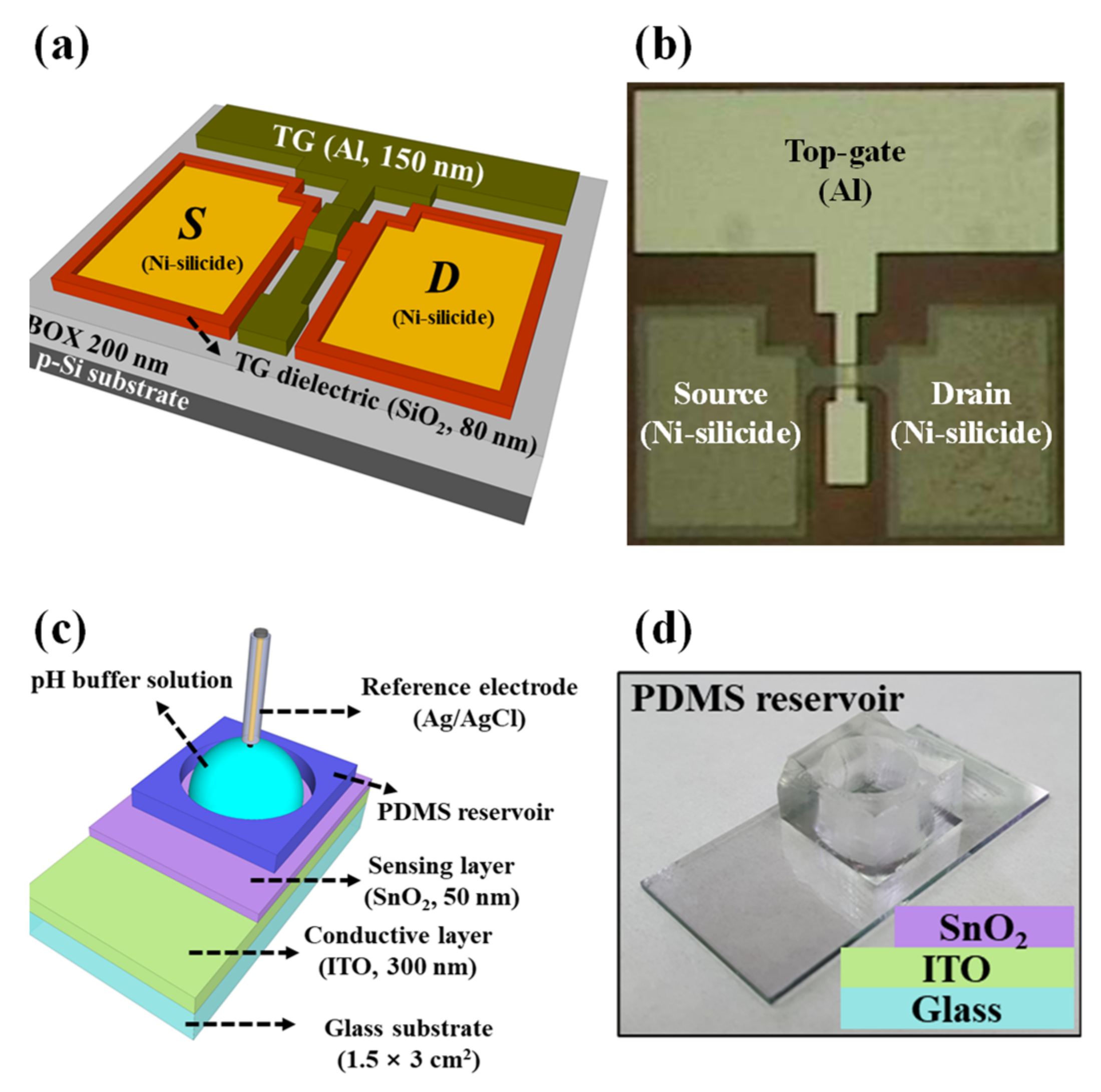
2.1. Fabrication of the Ambipolar DG ISFET and EG Unit

The proposed ambipolar DG ISFETs were fabricated on a silicon-on-insulator (SOI) substrate comprising a 100-nm-thick p-type top Si layer doped with 1 × 1015 cm−3 and a 200-nm-thick buried oxide layer. After removing the surface contaminants of the SOI substrate through RCA cleaning, the upper Si layer was etched with 2.38 wt.% tetramethylammonium hydroxide (TMAH) solution to prepare a 60-nm-thick, fully depleted SOI substrate. The active area of a FET transducer of length (L) and width (W) 20 µm and 10 µm, respectively, was defined by photolithography and plasma reactive ion etching (RIE) using SF6 gas.
After depositing a 150-nm-thick Ni layer using an electron beam evaporator, Ni was selectively left in the S/D region through a lift-off process. Then, using a 600 W MWI source for 2 min in an N2 ambient, Ni-silicide, which is a key material for bipolar switching, was formed [25]. Unreacted Ni was removed using a sulfur peroxide mixture (SPM) for 10 min. As the top-gate insulator, a 70-nm-thick SiO2 layer was deposited using an RF magnetron sputtering system. A 150-nm-thick Al film was deposited with an e-beam evaporator, followed by photolithography and wet etching by H3PO4 to form a top-gate electrode. The buried oxide layer of the SOI substrate serves as the bottom-gate insulator of the FET. Additionally, a 150-nm-thick Al film was deposited on the backside of the SOI substrate to form the bottom-gate electrode. After the local opening of the S/D contact for the holes in the top gate-oxide layer, a forming gas (H2:N2 = 5%:95%) annealing was performed for 30 min at 450 °C to improve the electrical characteristics of the ISFET.
Meanwhile, a separate EG unit was prepared to prevent deterioration owing to direct contact between the buffer solution and gate insulator of the FET transducer, which was fabricated on a 1.5 × 3 cm2 glass substrate. A 300-nm-thick indium tin oxide (ITO) conductive layer and a 50-nm-thick SnO2 sensing film were sequentially deposited on the glass substrate using an RF magnetron sputtering system. This layer acts as a receptor for the surface potential change and transfers the applied potential change. After the formation of the sensing layer, polydimethylsiloxane (PDMS) reservoir was attached with silicone glue for injecting the pH buffer solution. Figure 1 shows the schematic of the ambipolar DG ISFET and EG unit.

2.2. Characterization of the Fabricated Ambipolar DG ISFET

We evaluated the electrical properties of the fabricated bidirectional chemical sensor platform using an Agilent 4156B precision semiconductor parameter analyzer. The device was placed in a dark box to exclude optical and electrical interferences from the external environment. For the pH response analysis, a commercial ceramic-plug junction-type Ag/AgCl electrode (Horiba 2080-06T) with an internal solution AgCl-saturated KCl electrolyte was used as the reference electrode. In this experiment, we defined a reference voltage (VREF) at the ID of 100 pA (read current, IR) to quantify the amount of transfer characteristics (VG–ID) curve shift depending on the pH value of the buffer solution. Furthermore, the hysteresis and drift effects were measured, which indicated reliability degradation from repetitive and continuous operations. The hysteresis width voltage (VH) was determined from the VREF difference between the initial and final pH states in the loop path of pH 7 → 4 → 7 → 10 → 7. Additionally, the drift effect monitored the modulation of VREF when the SnO2 sensing membrane was exposed to a pH 7 buffer solution for 10 h.

2.3. Signal Amplification of the Ambipolar DG ISFET

For an ISFET with a DG structure, the sensing operation can be performed in either the SG mode, which measures the pH (or biosignal) of the target analyte using the top-gate electrode (reference electrode), or the DG mode, which measures the signal of the target analyte with the bottom-gate electrode. In the SG sensing mode, the bottom-gate electrode is grounded, and VG is swept for the top-gate electrode. At this time, the EG unit and reference electrode are located at the top-gate electrode, as shown in Figure 2a. Therefore, the shift of the VG–ID curve is determined only by the surface potential of the sensing membrane. The modulation of VREF in the top-gate operation ( Δ V REF T ), which quantitatively represents the degree of VG–ID curve shift, can be expressed as
Δ V R E F T = Δ φ
The pH sensitivity is limited to 59.14 mV/pH at room temperature owing to the site binding theory [8,26]. Therefore, the detection accuracy will be poor if the difference in concentrations is not significant. Similarly, in the DG sensing mode, the EG unit and reference electrode are connected to the top-gate electrode, and VG is swept for the bottom-gate electrode, as shown in Figure 2b. In this case, the pH sensitivity may exceed the sensitivity limit owing to the capacitive coupling effect between the top- and bottom-gate dielectric layers and is expressed as
Δ V R E F B = C t o x C b o x Δ φ = C t o x C b o x Δ V R E F T
where the modulation of VREF in the bottom-gate operation ( Δ V REF B ) is amplified by the capacitance ratio of the top to bottom gate dielectric layers [9,10,27]. Ctox and Cbox are the top- and bottom-gate dielectric capacitances, respectively. Δ V REF B and Δ V REF T are the reference voltage modulations of the top and bottom gates, respectively. In this study, considering that the top- and bottom-gate dielectrics are the same as SiO2, Equation (2) can be expressed according to the thickness ratio of the top- to bottom-gate dielectrics as
Δ V R E F B = t b o x t t o x Δ V R E F T
where ttox and tbox are the thicknesses of the top- and bottom-gate dielectrics, respectively.

3. Results and Discussion

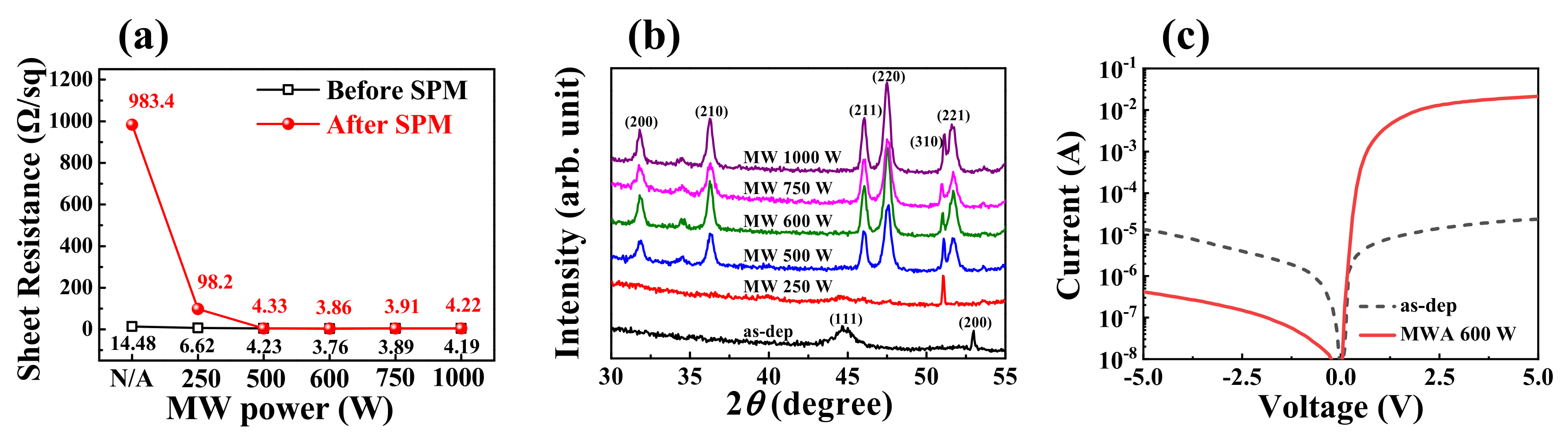
3.1. Evaluation of the Ni-Silicide S/D Region for Ambipolar DG ISFET

Ni-silicide is a typical midgap metal used in both NMOS and PMOS FETs, which enables ambipolar switching operations. In this study, a Ni-silicide SB S/D was formed with a low thermal budget through high-efficiency energy transfer of microwaves to implement an ambipolar DG ISFET with excellent electrical characteristics. Furthermore, to determine the optimal Ni-silicide formation conditions by MWI, we evaluated the electrical properties and crystallinity of the Ni-silicide layer based on microwave power. Figure 3a shows the sheet resistance (Rs) of the Ni-silicide layer under various microwave power conditions measured using a four-point probe. The MWI process for Ni silicidation was performed in an N2 ambient for 2 min, and the Rs was measured before and after removing the unreacted Ni using an SPM. Before SPM etching, because of the remaining Ni layer, all samples exhibited low Rs. Conversely, in the absence of MWI, the unreacted Ni was completely eliminated after SPM etching, which resulted in high Rs. However, above 250 W, the Rs decreases significantly after treatment with SPM and Ni-silicide formation is realized, whereas at 500 W, the decrease in Rs is almost saturated. It is worth noting that 600 W of MWI exhibits the lowest Rs. Therefore, 600 W was determined as the optimal condition in terms of resistance, thermal budget, and power consumption. Figure 3b shows the crystallinity of the characterized Ni-silicide layer by X-ray diffraction (XRD) analysis. The XRD pattern of the as-deposited Ni film showed peaks at (111) and (200) corresponding to pure Ni crystals. Conversely, after the silicidation process, several other peaks were observed. At a low microwave power of 250 W, a Ni-silicide peak corresponding to (310) was observed, indicating silicide formation. Meanwhile, several strong peaks corresponding to (211), (220), (310), (221), and (301) appeared above 500 W. Accordingly, we verified that Si and Ni reacted to form high-quality Ni-silicide through MWI treatment exceeding 500 W [28,29]. From the above results, an MWI of 600 W, which provides the lowest Rs and good crystallinity, was used for the Ni-silicide SB S/D formation in the fabrication of the ambipolar DG ISFET. Figure 3c shows the characterization of Schottky contact of S/D. The characteristic evaluation was performed through Schottky diodes. In the case of as-deposited Ni film, the rectification characteristics of the diodes are hardly exhibited due to the low on-current and high leakage current due to interfacial defects between the Si and unreacted Ni layers. On the other hand, in the Ni silicide junction diodes in which the silicide reaction occurred by 600 W MWI process, clear rectification characteristics of high on-current and low leakage current were observed.

3.2. Electrical Characteristics of the Ambipolar DG ISFET with Ni-Silicide SB S/D

The electrical characteristics of the FET transducer play an essential role in the pH sensing operation; hence, we measured the transfer characteristic (VG–ID) curves during the top- and bottom-gate operations to verify these characteristics. Figure 4 shows the electrical characteristics of the proposed device. Figure 4a shows the VG–ID curves for the top- and bottom-gate operations in the p- and n-regions, respectively. The drain voltages were −50 mV and 50 mV for the p- and n-regions, respectively. It is seen that the fabricated device exhibits distinct ambipolar conduction behaviors for the top- and bottom-gate operations. Furthermore, changing the polarity of the gate bias can cause the FET to behave as a p-type or an n-type channel. Additionally, the top gate allows a larger drive current compared to the bottom gate considering that the top-gate oxide is thinner than the bottom-gate oxide. Figure 4b shows the output characteristics (VD–ID) curves for the top- and bottom-gate operations in the p- and n-regions, respectively. For both the top- and bottom-gate operations, the drain current (ID) exhibited a pinch-off characteristic that increased linearly in the low drain voltage (VD) region before gradually saturating in the high VD region. Based on these transfer and output characteristics, we can confirm that the ambipolar DG FET transducer with Ni-silicide SB S/D was well-formed by the 600 W MWI process.

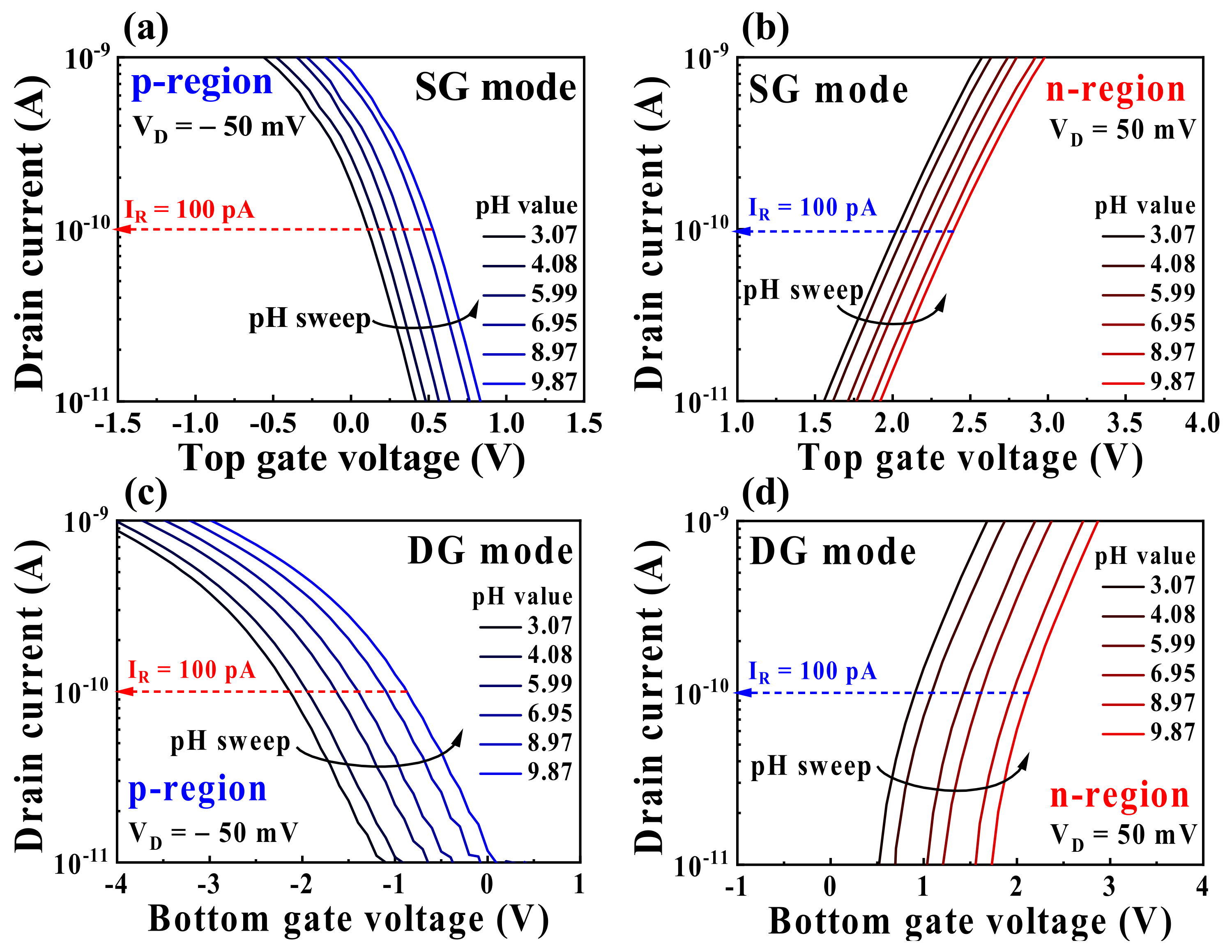
3.3. pH Sensing Performance of the Ambipolar DG ISFET

Generally, pH sensitivity is determined by the changes in the surface potential (Δφ) per unit pH value, where φ is defined by the ion concentration in the pH buffer solution, given as [8,26]:
φ = 2.303 k T q ( β β + 1 ) p H p z c p H  
where k is the Boltzmann constant, T is the absolute temperature, q is the elementary charge, pHpzc is the pH value at the point of zero charge, and β is the chemical sensitivity of the gate dielectric. Figure 5 shows the VG–ID curves of the ambipolar DG ISFET for different pH buffer solutions. The pH values of the buffer solutions used for the measurements were 3.07, 4.08, 5.99, 6.95, 8.97, and 9.87. Figure 5a,b show the sensing properties of the p and n regions in the SG sensing mode, respectively. In both cases, as the pH of the buffer solution increased, the transfer characteristic curve shifted toward the positive VG direction. Figure 5c,d show the shift of the VG–ID curve in the DG sensing mode. In this case, despite the same sensing membrane, the shift of the transfer curve is larger than that in the SG sensing mode. This indicates that the pH sensitivity is highly dependent on the transducer performance and quality of the sensing membrane. Since the DG ISFET is capacitively coupled between the top- and bottom-gate electrodes, it can self-amplify the sensitivity according to Equation (3) without the need for any additional amplification circuitry.
Figure 6 shows the shift in the reference voltage (ΔVREF) for the p and n regions as a function of the pH value. Herein, VREF was determined at a constant read drain current (IR) of 100 pA. The SG-mode pH sensitivities of the ambipolar sensor were 58.8 and 58.7 mV/pH in the p and n regions, respectively. According to the site coupling theory, the ISFET exhibits a low sensitivity of 59.14 mV/pH, whereas the proposed ambipolar sensor exhibits a sensitivity close to the Nernst limit in the SG sensing mode. Conversely, in the DG sensing mode, the pH sensitivities increased by approximately 3 times compared to those in the SG sensing mode. The extracted pH sensitivities were 177.5 and 175.0 m V/pH for the p and n regions, respectively; this magnification is almost identical to the potential increase by the amplification factor, ttox/tbox, in Equation (3).

3.4. Reliability and Stability of the Ambipolar DG ISFET

As both the pH sensitivity and reliability of the fabricated ambipolar ISFETs must be ensured for repeated and continuous operations, we evaluated the hysteresis and drift effects to derive the reliability in the SG and DG sensing modes. Figure 7 shows the hysteresis width voltage (VH) measurements when the sensing membrane undergoes a gradual change in the pH buffer solution. The sensing membrane of the EG unit comprises hydroxy groups, which are capable of capturing or releasing hydrogen ions. Although the surface of the sensing membrane is capable of fast bonding to hydrogen ions, the bulk exhibits slower bonding. This results in the degradation of reliability during the repetitive operation, called the hysteresis effect [30,31,32]. Measurements were conducted for a total of 50 min at intervals of 2 min and 10 min per buffer solution. The VH values obtained in the pH loop of 7 → 4 → 7 → 10 → 7 were 5.8 mV and 4.2 mV for the p and n regions, respectively, for the SG sensing mode and 8.6 mV and 5.1 mV, respectively, for the DG sensing mode.
During continuous operation for a long period, a hydration layer is formed on the surface of the sensing film, which diffuses ions of the electrolyte into the sensing membrane to alter its properties [30,33]. This results in a drift phenomenon accompanied by significant noise, which is considered a critical obstacle. Figure 8 shows the drift effect measurement when the EG is immersed in a pH 7 buffer solution for 10 h. The drift rates were 23.0 and 14.1 mV/h in the p and n regions, respectively, for the SG sensing mode and 30.2 and 18.3 mV/h, respectively, for the DG sensing mode. Although the differences in the drift rates were insignificant, the n-type operation was better compared to the p-type operation. As in the case of the hysteresis voltage, the drift rates of the SG and DG modes were much smaller than the sensitivities. The ratios of drift rate to sensitivity were 39.12% and 24.02% in the SG mode and 17.01% and 10.46% in the DG mode, respectively. These results mean that changing from the SG to DG mode increases the sensitivity by 201.87% and 198.13% and drift rates by only 31.3% and 29.79%, respectively. This indicates that in both the p and n channels, the stability and reliability are higher in the DG mode than in the SG mode owing to high sensitivity.
Table 1 summarizes the pH sensing performances of the proposed ambipolar DG ISFETs. The fabricated device exhibits amplified sensitivity depending on the capacitance ratio of the top- to bottom-gate electrodes. Specifically, it is worth noting that the increase in nonideal behavior is significantly lower than the amplification of sensitivity, which indicates that the proposed bidirectional chemical sensor platform is capable of amplification with guaranteed reliability and stability, along with operating as a p-type device with good noise resistance or an n-type device with good mobility and drift performance.
Finally, the ISFET inverter is considered as a potential application of the proposed bipolar ISFET. However, there are some applications where analog details are not required, and simply determining whether the chemical concentration or pH is above or below a certain threshold is sufficient. In particular, for DNA sequencing where a “yes”/”no” answer to the pH change is sufficient, an ISFET inverter can determine whether a chain extension reaction has occurred [34,35]. Fabricating a typical ISFET inverter requires a CMOS process where n-type and p-type dopants are implanted and activated. This process is complex and time-consuming, resulting in high fabrication costs. However, the proposed ambipolar ISFET does not require doping of the n-type and p-type impurities and is easy to implement in a CMOS-like inverter with simple silicide formation. Therefore, the CMOS-like inverter based on the proposed ambipolar ISFET may be a promising candidate for DNA logic gates.

4. Conclusions

This study proposes a high-performance bidirectional chemical sensor platform based on ambipolar DG ISFETs with microwave-assisted Ni-silicide SB S/D and a separative EG unit. The proposed device exhibits ambipolar switching and excellent electrical characteristics as a transducer. Furthermore, the fabricated bipolar chemical sensor platform exhibits pH sensitivities of 58.8 and 58.7 mV/pH in the p- and n-regions, respectively, in the SG sensing mode compared to the theoretical limit of sensitivity at room temperature. Conversely, we achieved excellent pH sensitivities of 177.5 and 175.0 mV/pH in the p- and n-regions, respectively, in the DG sensing mode, which is approximately three times that achieved in the SG sensing mode, owing to the capacitive coupling effect between the top and bottom gates. The VH values were 5.8 mV and 4.2 mV in the p- and n-regions, respectively, in the SG sensing mode and 8.6 mV and 5.1 mV, respectively, in the DG sensing mode. Additionally, the drift rates were 23.0 mV/h and 14.1 mV/h in the p- and n-regions, respectively, in the SG sensing mode and 30.2 mV/h and 18.3 mV/h, respectively, in the DG sensing mode. Although the DG mode has larger VH and drift rates compared to the SG mode, the increase in nonideal effects was found to be relatively small compared to the sensitivity amplification ratio. Thus, the application of Ni-silicide S/D and DG structures enables bidirectional sensing operation of the p- and n-channels depending on the purpose of use while ensuring high sensitivity and stability. In addition to these advantages, the proposed bidirectional chemical sensor platform, which has a simple process and bidirectional operation capability, is expected to be applicable in various fields including biosensors. Furthermore, when subsequent study containing bio-selective elements is introduced, it will be possible to implement a biological event monitoring system that can detect regardless of the polarity of the target substance and secure high sensitivity.

Author Contributions

Y.-U.K.: conceptualization, formal analysis, methodology, investigation, data curation, visualization, software, resources, and writing—original draft. W.-J.C.: conceptualization, methodology, investigation, resources, formal analysis, funding acquisition, supervision, validation, and writing—review and editing. All authors have read and agreed to the published version of the manuscript.

Funding

This work was supported by the National Research Foundation of Korea (NRF) grant funded by the Korean government (MSIT) (No. 2020R1A2C1007586).

Institutional Review Board Statement

Not applicable.

Informed Consent Statement

Not applicable.

Data Availability Statement

Not applicable.

Acknowledgments

The present Research has been conducted by the Research Grant of Kwangwoon University in 2022 and the Excellent research support project of Kwangwoon University in 2022.

Conflicts of Interest

The authors declare no conflict of interest.

References

  1. Ndiaye, M.; Oyewobi, S.S.; Abu-Mahfouz, A.M.; Hancke, G.P.; Kurien, A.M.; Djouani, K. IoT in the wake of COVID-19: A survey on contributions, challenges and evolution. IEEE Access 2020, 8, 186821–186839. [Google Scholar] [PubMed]
  2. Giwan, S.; Geonhee, L.; Mi, J.K.; Seung-Hwa, B.; Minsuk, C.; Keun, B.K.; Chang-Seop, L.; Sangmi, J.; Deaui, P.; Hong, G.K.; et al. Rapid detection of COVID-19 causative virus (SARS-CoV-2) in human nasopharyngeal swab specimens using a field-effect transistor-based biosensor. ACS Nano 2020, 14, 5135–5142. [Google Scholar]
  3. Abdulhadee, Y.; Umaporn, P.; Sirirat, R.; Nattiya, H.; Orawon, C.; Sudkate, C. Paper-based electrochemical biosensor for diagnosing COVID-19: Detection of SARS-CoV-2 antibodies and antigen. Biosens. Bioelectron. 2021, 176, 112912. [Google Scholar]
  4. Kim, S.; Ahn, J.H.; Park, T.J.; Lee, S.Y.; Choi, Y.K. A biomolecular detection method based on charge pumping in a nanogap embedded field-effect-transistor biosensor. Appl. Phys. Lett. 2009, 94, 243903. [Google Scholar]
  5. Tsai, C.-C.; Chiang, P.-L.; Sun, C.-J.; Lin, T.-W.; Tsai, M.-H.; Chang, Y.-C.; Chen, Y.-T. Surface potential variations on a silicon nanowire transistor in biomolecular modification and detection. Nanotechnology 2011, 22, 135503. [Google Scholar]
  6. Bergveld, P. Thirty years of ISFETOLOGY: What happened in the past 30 years and what may happen in the next 30 years. Sens. Actuators B Chem. 2003, 88, 1–20. [Google Scholar]
  7. Sadighbayan, D.; Hasanzadeh, M.; Ghafar-Zadeh, E. Biosensing based on field-effect transistors (FET): Recent progress and challenges. Trends Anal. Chem. 2020, 133, 116067. [Google Scholar]
  8. Bergveld, P. Development of an ion-sensitive solid-state device for neurophysiological measurements. IEEE. Trans. Biomed. Eng. 1970, 1, 70–71. [Google Scholar]
  9. Li, B.-R.; Chen, C.-W.; Yang, W.-L.; Lin, T.-Y.; Pan, C.-Y.; Chen, Y.-T. Biomolecular recognition with a sensitivity-enhanced nanowire transistor biosensor. Biosens. Bioelectron. 2013, 45, 252–259. [Google Scholar]
  10. Cho, S.-K.; Cho, W.-J. High-sensitivity pH sensor based on coplanar gate AlGaN/GaN metal-oxide-semiconductor high electron mobility transistor. Chemosensors 2021, 9, 4213. [Google Scholar]
  11. Jang, H.J.; Cho, W.J. Performance enhancement of capacitive-coupling dual-gate ion-sensitive field-effect transistor in ultra-thin-body. Sci. Rep. 2014, 4, 1–8. [Google Scholar]
  12. Ioannidis, E.G.; Theodorou, C.G.; Haendler, S.; Josse, E.; Dimitriadis, C.A.; Ghibaudo, G. Impact of source–drain series resistance on drain current mismatch in advanced fully depleted SOI n-MOSFETs. IEEE Electron. Device Lett. 2015, 36, 433–435. [Google Scholar]
  13. Rahhal, L.; Bajolet, A.; Diouf, C.; Cros, A.; Rosa, J.; Planes, N.; Ghibaudo, G. New methodology for drain current local variability characterization using Y function method. In Proceedings of the 2013 IEEE International Conference on Microelectronic Test Structures (ICMTS), Osaka, Japan, 25–28 March 2013; pp. 99–103. [Google Scholar]
  14. Dubois, E.; Larrieu, G. Low Schottky barrier source/drain for advanced MOS architecture: Device design and material considerations. Solid State Electron. Lett. 2002, 46, 997–1004. [Google Scholar]
  15. Hwang, H.; Lee, D.-H.; Hwang, J.M. Degradation of MOSFETs drive current due to halo ion implantation. Tech. Dig. Int. Electron. Devices Meet. 1996, 4, 567–570. [Google Scholar]
  16. Won-Jae, L.; Do-Woo, K.; Soon-Young, O.; Yong-Jin, K.; Ying-Ying, Z.; Zhun, Z.; Shi-Guang, L.; Soon-Yen, J.; In-Sik, H.; Tae-Kyu, G. Work function variation of nickel silicide using an ytterbium buffer layer for Schottky barrier metal-oxide-semiconductor field-effect transistors. Int. J. Appl. Phys. 2007, 101, 103710. [Google Scholar]
  17. Seger, J.; Hellström, P.E.; Lu, J.; Malm, B.G.; von Haartman, M.; Östling, M.; Zhang, S.L. Lateral encroachment of Ni-silicides in the source/drain regions on ultrathin silicon-on-insulator. Appl. Phys. Lett. 2005, 86, 253507. [Google Scholar]
  18. Xu, Z.; Zi, W.; Ruxin, S.; Yadan, Z.; Lunan, Z.; Di, X.; Lizhen, H.; Lifeng, C. High performance gas sensors with dual response based on organic ambipolar transistors. J. Mater. Chem. C 2021, 9, 1584–1592. [Google Scholar]
  19. Ajay, S.; Rakhi, N.; Manoj, S.; Mridula, G. Ambipolar behaviour of tunnel field effect transistor (TFET) as an advantage for biosensing applications. In Physics of Semiconductor Devices; Springer: Berlin/Heidelberg, Germany, 2014; pp. 171–174. [Google Scholar]
  20. Yuan, L.; Guo, Z.; Hailong, Z.; Zheng, L.; Rui, C.; Yang, X.; Vincent, G.; Yu, H.; Xiangfeng, D. Ambipolar barristors for reconfigurable logic circuits. Nano Lett. 2017, 17, 1448–1454. [Google Scholar]
  21. Jakobson, C.G.; Nemirovsky, Y. 1/f noise in ion sensitive field effect transistors from subthreshold to saturation. IEEE Trans. Electron. Devices 1999, 46, 259–261. [Google Scholar]
  22. Panahi, A.; Sadighbayan, D.; Forouhi, S.; Ghafar-Zadeh, E. Recent advances of field-effect transistor technology for infectious diseases. Biosensors 2021, 11, 103. [Google Scholar]
  23. Schmitt, A.L.; Higgins, J.M.; Szczech, J.R.; Jin, S. Synthesis and applications of metal silicide nanowires. J. Mater. Chem. 2010, 20, 223–235. [Google Scholar]
  24. Byon, K.; Tham, D.; Fischer, J.E.; Johnson, A.T. Systematic study of contact annealing: Ambipolar silicon nanowire transistor with improved performance. Appl. Phys. Lett. 2007, 90, 143513. [Google Scholar]
  25. Min, J.G.; Lee, D.H.; Kim, Y.U.; Cho, W.J. Implementation of ambipolar polysilicon thin-film transistors with nickel silicide Schottky junctions by low-thermal-budget microwave annealing. Nanomaterials 2022, 12, 628. [Google Scholar]
  26. Yates, D.E.; Levine, S.; Healy, T.W. Site-binding model of the electrical double layer at the oxide/water interface. J. Chem. Soc. Faraday Trans. 1974, 70, 1807–1818. [Google Scholar]
  27. Jang, H.J.; Cho, W.J. Fabrication of high-performance fully depleted silicon-on-insulator based dual-gate ion-sensitive field-effect transistor beyond the Nernstian limit. Appl. Phys. Lett. 2012, 100, 073701. [Google Scholar]
  28. Bhaskaran, M.; Sriram, S.; Mitchell, D.R.G.; Short, K.T.; Holland, A.S.; Mitchell, A. Effect of multi-layered bottom electrodes on the orientation of strontium-doped lead zirconate titanate thin films. Micron 2008, 40, 11–14. [Google Scholar]
  29. Wen-Li, C.; Chung-Hua, C.; Jui-Yuan, C.; Chun-Wei, H.; Yu-Ting, H.; Kuo-Chang, L.; Cheng-Lun, H.; Ping-Hung, Y.; Wen-Wei, W. Single-crystalline δ-Ni2Si nanowires with excellent physical properties. Nanoscale Res. Lett. 2013, 8, 1–5. [Google Scholar]
  30. Chou, J.C.; Wang, Y.F. Preparation and study on the drift and hysteresis properties of the tin oxide gate ISFET by the sol–gel method. Sens. Actuators B Chem. 2002, 86, 58–62. [Google Scholar]
  31. Bousse, L.; Mostarshed, S.; van der Schoot, B.; De Rooij, N.F. Comparison of the hysteresis of Ta2O5 and Si3N4 pH-sensing insulators. Sens. Actuators B Chem. 1994, 17, 157–164. [Google Scholar]
  32. Bousse, L.; Bergveld, P. The role of buried OH sites in the response mechanism of inorganic-gate pH-sensitive ISFETs. Sens. Actuators 1984, 6, 65–78. [Google Scholar]
  33. Chou, J.C.; Hsiao, C.N. The hysteresis and drift effect of hydrogenated amorphous silicon for ISFET. Sens. Actuators B Chem. 2000, 66, 181–183. [Google Scholar]
  34. Al-Ahdal, A.; Toumazou, C. ISFET-based chemical switch. IEEE Sens. J. 2011, 12, 1140–1146. [Google Scholar]
  35. Wong, W.; Shepherd, L.; Georgiou, P.; Toumazou, C. Towards ISFET based DNA logic for rapid nucleic acid detection. Sensors 2009, 8, 1451–1454. [Google Scholar]
Figure 1. (a) Schematic and (b) microscopic image of ambipolar DG ISFET with Ni-silicide SB S/Ds on an SOI substrate. (c) Schematic and (d) photograph of the fabricated EG unit.
Chemosensors 10 00122 g001
Figure 2. Simplified schematics of the DG ISFET sensor platform.
Chemosensors 10 00122 g002
Figure 3. (a) Sheet resistance (Rs) and (b) XRD patterns of the microwave-assisted Ni-silicides formed under various MWI powers. (c) The characterization of Schottky contact of S/D.
Chemosensors 10 00122 g003
Figure 4. Transfer characteristic (VG–ID) curves of the bipolar DG ISFETs operated by the top- or bottom-gate voltages in the (a) p and n regions. (b) Output characteristic (VD–ID) curves of the bipolar DG ISFETs operated by the top- or bottom-gate voltages in the p and n regions, respectively.
Chemosensors 10 00122 g004
Figure 5. Transfer characteristic (VG–ID) curves of the ambipolar DG ISFET for different pH buffer solutions. SG mode sensing in the (a) p region and (b) n region. DG mode sensing in the (c) p region and (d) n region.
Chemosensors 10 00122 g005
Figure 6. Reference voltage shift (ΔVREF) in the (a) p- and (b) n-region operations as a function of the pH value. The symbols and lines represent the experimental data and linear fits, respectively.
Chemosensors 10 00122 g006
Figure 7. Hysteresis effect of the ambipolar DG ISFET in the (a) p region and (b) n region for three different buffer solutions with pH values of 4, 7, and 10. The open and closed circles represent ΔVREF in the SG and DG sensing modes, respectively.
Chemosensors 10 00122 g007
Figure 8. Drift effects of the ambipolar DG ISFET in the (a) p region and (b) n region when the sensing membrane is immersed in a pH 7 buffer for 10 h. ΔVREF was monitored in the SG and DG sensing modes.
Chemosensors 10 00122 g008
Table 1. pH sensing performance of the fabricated bipolar DG ISFETs.
Sensitivity (mV/pH)VH
(mV)
Drift Rate (mV/h)
p-regionSG mode58.85.823.0
DG mode177.58.630.2
n-regionSG mode58.74.214.1
DG mode175.05.118.3
Publisher’s Note: MDPI stays neutral with regard to jurisdictional claims in published maps and institutional affiliations.

