Article

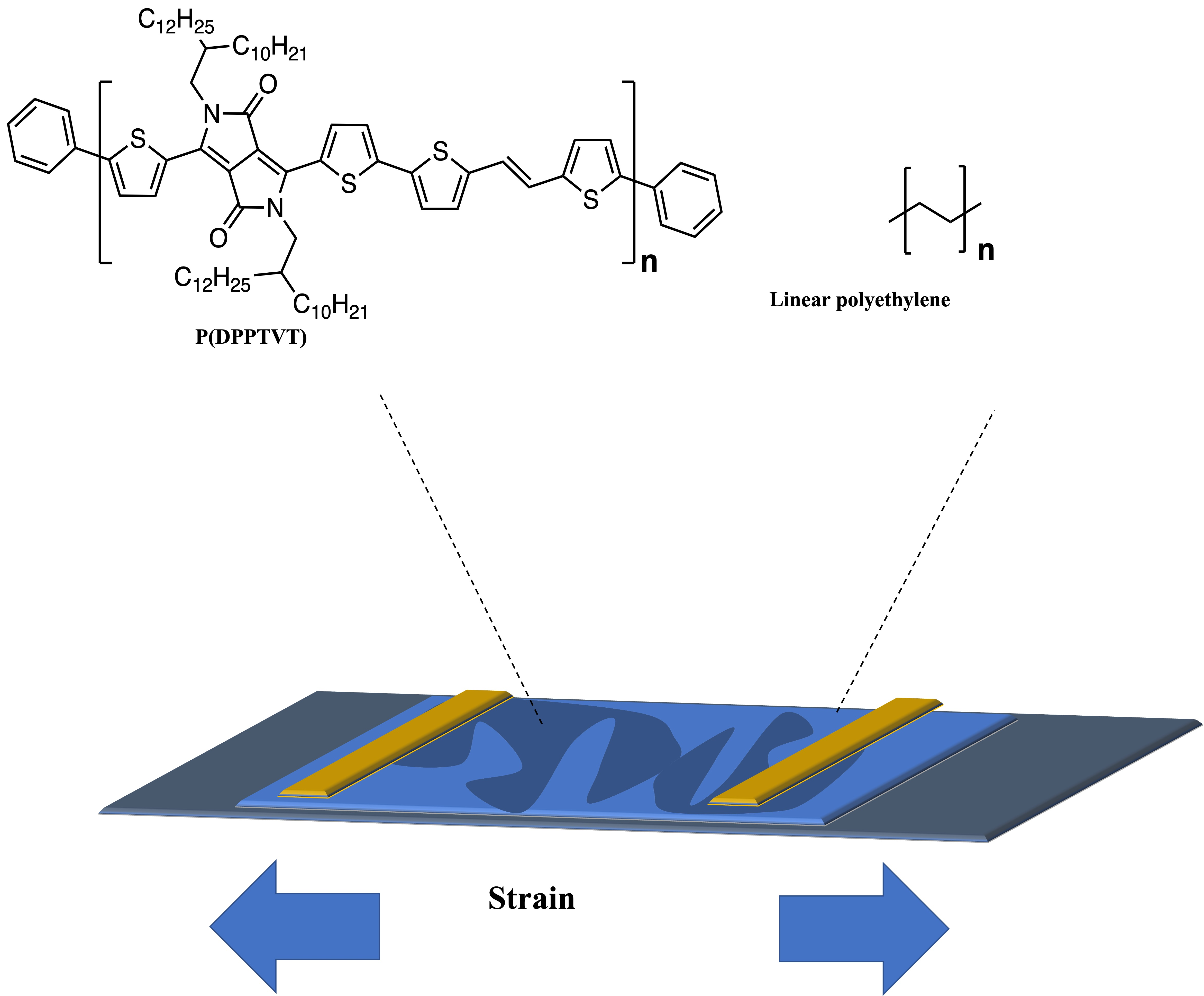
Polyethylene and Semiconducting Polymer Blends for the Fabrication of Organic Field-Effect Transistors: Balancing Charge Transport and Stretchability

by
Piumi Kulatunga
,
Nastaran Yousefi
and
Simon Rondeau-Gagné
*
Department of Chemistry and Biochemistry, University of Windsor, Windsor, ON N9B 3P4, Canada
*
Author to whom correspondence should be addressed.
Submission received: 26 April 2022 / Revised: 16 May 2022 / Accepted: 20 May 2022 / Published: 24 May 2022
(This article belongs to the Special Issue Functionalized Organic Thin Film Transistors for Sensing)

Abstract

:
Polyethylene is amongst the most used polymers, finding a plethora of applications in our lives owing to its high impact resistance, non-corrosive nature, light weight, cost effectiveness, and easy processing into various shapes from different sizes. Despite these outstanding features, the commodity polymer has been underexplored in the field of organic electronics. This work focuses on the development of new polymer blends based on a low molecular weight linear polyethylene (LPE) derivative with a high-performance diketopyrrolopyrrole-based semiconducting polymer. Physical blending of the polyethylene with semiconducting polymers was performed at ratios varying from 0 to 75 wt.%, and the resulting blends were carefully characterized to reveal their electronic and solid-state properties. The new polymer blends were also characterized to reveal the influence of polyethylene on the mechanical robustness and stretchability of the semiconducting polymer. Overall, the introduction of LPE was shown to have little to no effect on the solid-state properties of the materials, despite some influence on solid-state morphology through phase separation. Organic field-effect transistors prepared from the new blends showed good device characteristics, even at higher ratios of polyethylene, with an average mobility of 0.151 cm2 V−1 s−1 at a 25 wt.% blend ratio. The addition of polyethylene was shown to have a plasticizing effect on the semiconducting polymers, helping to reduce crack width upon strain and contributing to devices accommodating more strain without suffering from decreased performance. The new blends presented in this work provide a novel platform from which to access more mechanically robust organic electronics and show promising features for the utilization of polyethylene for the solution processing of advanced semiconducting materials toward novel soft electronics and sensors.

Graphical Abstract

1. Introduction

Polymer blending is a very common and efficient approach to fine-tune the properties of polymers [1,2,3]. Through careful selection of the blend partners, it is possible to engineer not only the microstructure of the resulting blends, but also to optimize a plethora of material properties, including their optical, electronic, and mechanical properties [4,5,6]. While being a very common approach for the preparation of commodity polymers (elastomers, thermosets, and thermoplastics) at the industrial scale, this approach has also been recently developed and investigated in the field of organic electronics [7,8,9]. For emerging electronics, based on the utilization of organic materials, the blending of the electroactive component with soft and/or insulating polymers has proved to be a very effective and promising approach to control the properties of the materials in thin films, particularly by promoting phase separation and the nanoscale confinement of the semiconducting materials [10,11]. This particular phase morphology was shown in multiple reports to be advantageous for charge transport in organic electronic devices, but also to help the materials to sustain deformation upon mechanical strain [12,13].
Among the recent examples of semiconducting polymer blend systems for applications in organic electronics, the utilization of styrene-ethylene-butylene-styrene (SEBS) has been shown to be particularly effective for promoting nanoscale phase separation of high-performance semiconducting polymers [12,14,15]. As shown in the literature, the blending of semiconducting polymers with SEBS can not only enhance charge transport in organic field-effect transistors, but also help the materials to sustain strain up to 120% elongation without a significant decrease in performance. Polydimethylsiloxane (PDMS) [16] and polyisobutylene (PIB) [17] are also two soft polymers that can effectively improve the mechanical properties of polythiophene- and polydiketopyrrolopyrrole (DPP)-based semiconducting polymers when blended and processed in thin films. Other recent examples from our group and others explored various types of polymers for the blending with semicrystalline semiconducting polymers including polystyrene and polyurethane-PDMS copolymers [18,19].
While many reports have focused on the utilization of soft insulating elastomers for the development of stretchable semiconducting polymer blends, little attention has been paid to polyethylene even though this material possesses many interesting features that can make it a good candidate for the further development of this strategy. Among the different thermoplastics, polyethylene (PE) is undoubtedly the most used polymer, having a wide range of applications due to properties such as its high impact resistance, non-corrosive nature, light weight, cost effectiveness, and easy processing into various shapes from different sizes (tunability) [20,21,22,23]. All these important features are desirable for the development of new advanced and emerging electronics.
Recently, our team investigated a novel type of hyperbranched polyethylene (BPE) material with very promising properties, including a low boiling point and strong interactions with DPP-based semiconducting polymers [24]. These specific advantages have motivated our team to exploit BPE as an additive or solvent in conjunction with semiconducting materials. Overall, our work has shown that BPE can be blended with conjugated materials to induce nanophase separation in the solid state. The resulting composite provides good charge mobilities in field-effect transistors. At the same time, BPE can act as a plasticizer to provide mechanical softness and stretchability to the composite [25]. BPE has also been used as a solvent to replace chlorinated solvents for the fabrication of organic field-effect transistor (OFET) devices [26]. Despite these interesting features, BPE has some challenging limitations. Its synthesis requires many steps, and the resulting materials often lack chemical functional diversity, limiting the possibilities in polymer blends due to suboptimal miscibility with conjugated polymers. Furthermore, its low boiling point (below 150 °C) can be detrimental to the stability of the devices through changes in microstructure over time.
Herein, we report on the blending of a semicrystalline DPP-based polymer, P(DPPTVT), with a linear polyethylene (LPE) derivative. In contrast to previous work on BPE, the LPE was chosen to be non-volatile and to possesses a linear structure, thus allowing for the formation of stable and highly tunable semiconducting polymer-polyethylene blends. In addition to a careful optimization of the blend miscibility and the thin-film formation process, the resulting blends were carefully characterized to unveil the influence of LPE on the optoelectronic and solid-state properties of the materials. At ratios between 25 and 75 wt.%, LPE was shown to promote a moderate phase separation with the conjugated polymers, thus leading to an enhanced aggregation in the solid state as probed by UV-vis spectroscopy. The blending of P(DPPTVT) with LPE at 25 wt.% was shown not to decrease charge transport, as observed through the fabrication of OFET devices. In addition to the optoelectronic, charge transport, and solid-state properties, the mechanical properties of the new polymer blends were investigated through various techniques, including atomic force microscopy (AFM) and grazing-incidence X-ray diffraction (GIXRD). The blending of the semiconducting polymer with LPE was shown to progressively help to improve the mechanical properties of the semiconductor in thin film by diminishing crack dimensions upon strain. Moreover, the blending with LPE enabled the semiconducting polymer to maintain its initial charge mobilities in OFETs after stretching at 25% strain elongation. Overall, the results described in this report confirm the efficiency of the blending of semiconducting polymers with soft materials for the fabrication of mechanically robust electronics. Furthermore, the study introduces a new strategy with which to exploit the chemical and synthetic versatility of commodity polymers for application in advanced electronics manufacturing.

2. Experimental Section

2.1. Materials

Commercial reactants were used without further purification unless stated otherwise. All the solvents used in these reactions were distilled prior to use. Linear polyethylene (Mn = 1700 Da) was purchased from Sigma Aldrich. Tris(dibenzylideneacetone)-dipalladium(0)-chloroform adduct (Pd2(dba)3·CHCl3) was purchased from Sigma Aldrich (Burlington, VT, USA) and recrystallized following a reported procedure [27]. (E)-1,2-bis(5-(Trimethylstannyl)thiophen-2-yl)ethene (TVT) and 3,6-bis(5-bromothiophen-2-yl)-2,5-bis(2-decyltetradecyl)-2,5-dihydropyrrolo[3,4-c]pyrrole-1,4-dione were synthesized according to the literature [28], resulting in a polymer with Mn = 33 kDa, Mw = 44 kDa and Đ = 1.38.

2.2. Measurements and Characterization

Number average molecular weight (Mn), weight average molecular weight (Mw), and dispersity (Đ) were evaluated by high-temperature size exclusion chromatography (SEC) using 1,2,4-trichlorobenzene and performed on an EcoSEC HLC-8321GPC/HT (Tosoh Bioscience, Tokyo, Japan) equipped with a single TSK gel GPC column (GMHHR-H; 300 mm × 7.8 mm) calibrated with monodisperse polystyrene standards.
Morphology of polymer blends was assessed using a multimode atomic force microscope (AFM, digital instruments) operated in the tapping mode at room temperature. Images were collected using Nanoscope 6 software and processed using Nanoscope analysis software. UV-visible spectroscopy was performed on a Varian UV/Visible Cary 50 spectrophotometer. Grazing-incidence X-ray diffraction (GIXRD) was performed at the Canadian Light Source at beamline BXDS-WLE. The X-ray wavelength was 0.8200 Å or a beam energy of 15.120 keV. The incidence angle of X-rays was set at 0.10 and the sample to detector distance was about 500 mm. Numerical integration of the diffraction peak areas was performed using the software Igor. All the measurements of the transistors were conducted using a Keithley 4200 semiconductor parameter analyzer (Keithley Instruments Inc., Cleveland, OH, USA) under dry N2 (glovebox) and at room temperature.

2.3. Polymer Blend Preparation

Polymer blends were prepared by dissolving the conjugated polymer and linear polyethylene (LPE) in 2 mL of chlorobenzene according to different weight ratios and heated to 90 °C overnight. For all the blends, 3 mg of conjugated polymer was used. Amounts of 0, 25, 50, and 75 wt.% polymer blends were prepared by adding 0, 1, 3 and 9 mg of LPE, respectively.

2.4. Device Fabrication and Characterization

OFET devices were fabricated on highly doped n-type Si (100) wafers with 300 nm thick SiO2 functionalized with an n-octadecyltrimethoxysilane (OTS) self-assembled monolayer, according to the reported method [29]. The OTS-treated substrate was washed with toluene, acetone, and isopropanol, and then dried with nitrogen before use. Next, polymer solutions were spin cast on OTS-coated Si wafers at 2000 rpm for 1 min. Samples were thermally annealed using a hot plate at 90 °C and 150 °C inside a N2-filled glove box. Source and drain top electrodes were then deposited by evaporating gold (≈50 nm) through a shadow mask with a channel length (L) and width (W) defined as 150 and 1000 μm, respectively. A shadow mask with a channel length (L) and width (W) defined as 100 and 1000 μm, respectively, was used for stretched devices. All measurements were conducted using a Keithley 4200-SCS semiconductor parameter analyzer (Keithley Instruments Inc., Cleveland, OH, USA) in a N2-filled glove box at room temperature.

2.5. Transfer-Printed Organic Field-Effect Transistor Fabrication

To measure the charge mobilities upon stretching, a lamination procedure adapted from previous literature was used to laminate the semiconducting polymer films onto PDMS [30]. The resulting thin films supported on PDMS were stretched to 25% strain and laminated back to Si wafers. Source and drain top electrodes were deposited parallel and perpendicular to the stretching direction by evaporating gold (≈50 nm) through a shadow mask with a channel length (L) and width (W) defined as 100 and 1000 μm, respectively. All measurements were conducted using a Keithley 4200-SCS semiconductor parameter analyzer (Keithley Instruments Inc., Cleveland, OH, USA) in a N2-filled glove box at room temperature.

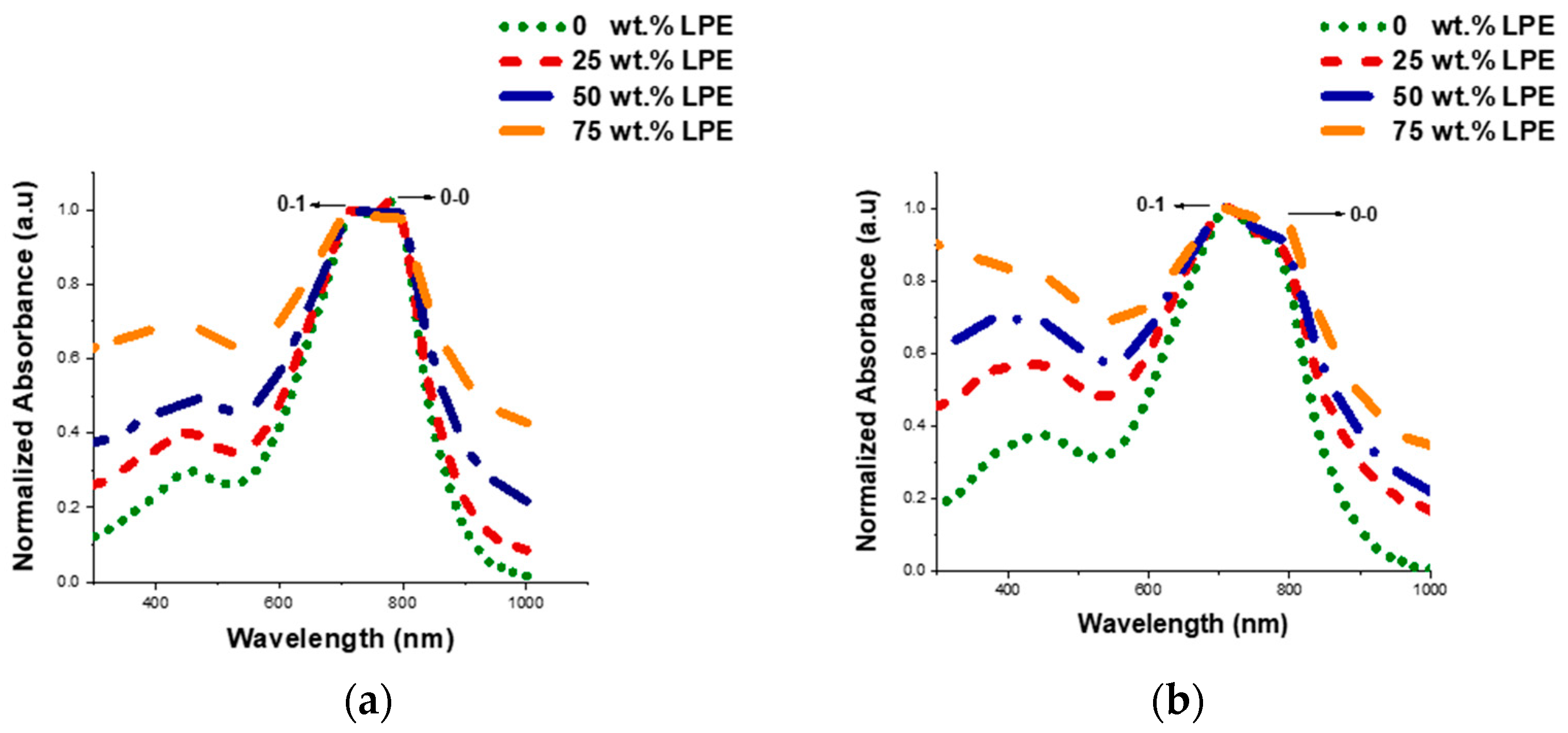
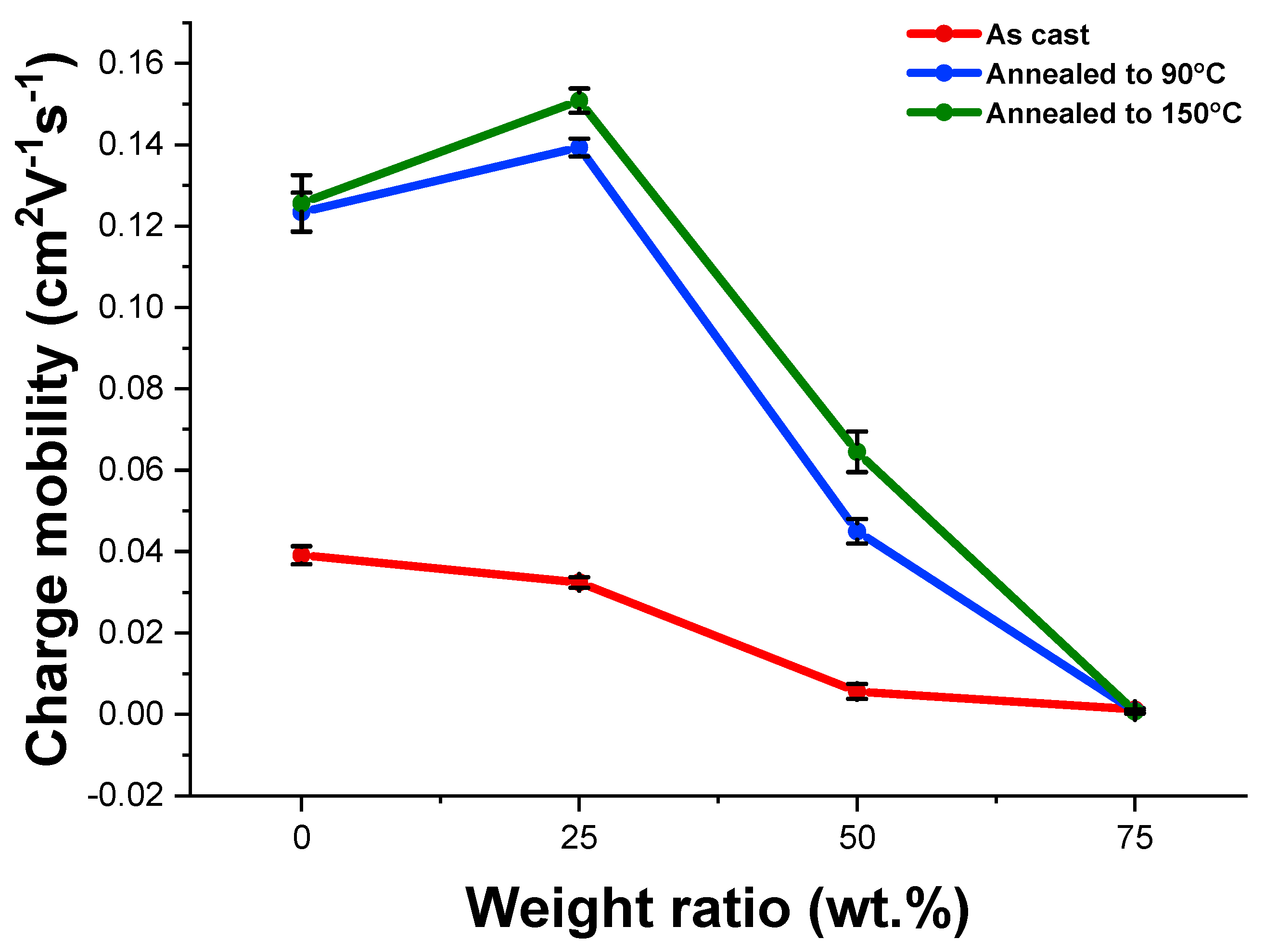
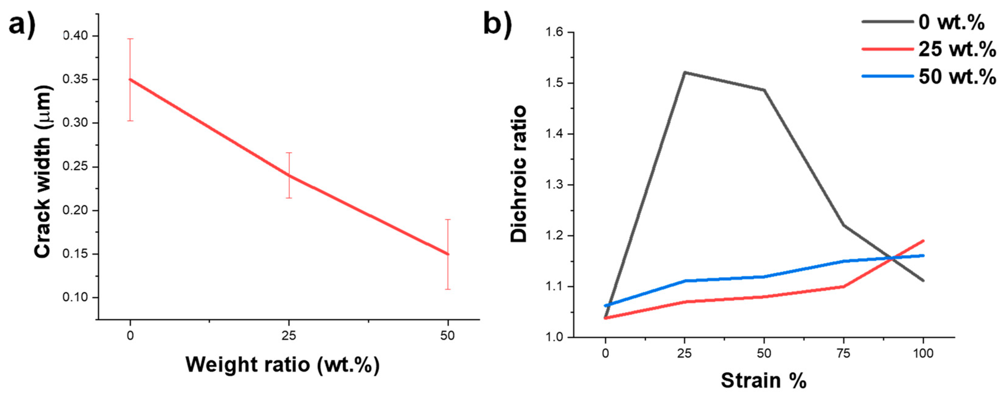
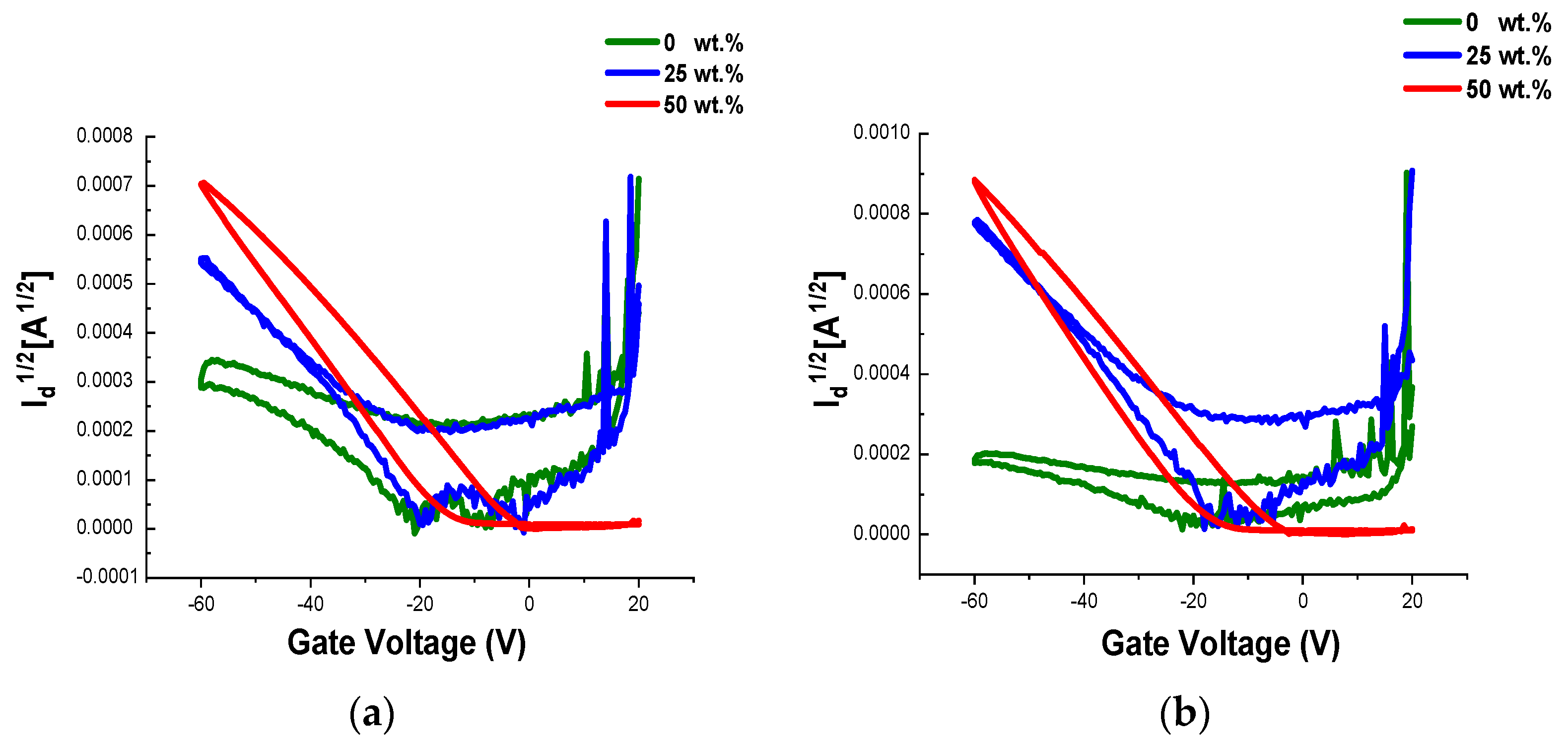
3. Results and Discussion

In order to gain insights into the influence of linear polyethylene on several key properties of semiconducting polymers, a selected DPP-based polymer, namely P(DPPTVT), was blended at different weight ratios with a commercially-available linear polyethylene (LPE). The semiconducting polymer was selected due to its previously reported high charge carrier mobility in OFETs, and the polymer was prepared through a known procedure [8,31,32,33]. All the details about material synthesis and sample preparation are available in the Supplementary Information.
To understand the aggregation behavior of these polymer blends and investigate their optical properties in solution and solid states, UV-vis spectroscopy was employed. UV-vis spectra for polymer blends (ranging from 0 to 75 wt.% LPE) were collected for solution and solid (thin film) states before and after annealing at 150 °C (Figure 1, Figures S1 and S2). As shown in Figure 1, there are two distinct absorption bands present in all the solid-state spectra, which are typically observed in donor–acceptor π-conjugated semiconducting polymer systems [34]. The absorption band around λ = 400 nm is associated with π–π* transition, whereas the one centered at λ = 750 nm corresponds to the donor–acceptor charge transfer. The extent of the intramolecular and intermolecular interactions (aggregation) can be determined using the ratio of the vibrational peak intensities ( A 0 0 / A 0 1 ) present around λ = 750 nm [35]. Based on the UV-vis results reported in Figure S1, there is not a significant change in the A 0 0 / A 0 1 ratio upon the addition of LPE to the system in solution. This observation indicates that the addition of LPE up to 75 wt.% does not influence the molecular aggregation in the solution state. Additionally, the UV-vis spectra of P(DPPTVT) blends with 0–75 wt.% LPE were collected for thin films. As shown in Figure 1a, the change in A 0 0 / A 0 1 ratio is minimal, indicating only a slight increase in molecular aggregation with the addition of 75 wt.% LPE. To investigate the influence of annealing on the molecular aggregation, thin films of blend polymers were annealed at 150 °C for 30 min. As shown in Figure 1b, the A 0 0 / A 0 1 ratio remained unchanged for most of the blend ratios, proving that the addition of LPE does not interrupt the molecular aggregation of P(DPPTVT) significantly. However, the highest change in the molecular aggregation was shown for the 75 wt.% LPE blends after annealing (Figure 1b). This observation is in contrast with other blend systems where the addition of insulating polymer often resulted in the promotion of interchain aggregation [12,24].
It is anticipated that the charge transport decreases upon the physical blending of a semiconducting polymer with an insulating soft polymer [36]. To tune charge carrier mobilities, careful control over phase morphology and phase separation in the solid state is necessary to ensure a pathway for charges to percolate across the polymer network. To visualize the solid-state microstructure of P(DPPTVT) upon progressive addition of LPE, we used atomic force microscopy (AFM). The results are depicted in Figures S3–S5, revealing both phase and height profiles of thin films upon addition of LPE to P(DPPTVT). In order to investigate the influence of annealing temperature on the solid-state morphology of the polymer blends, the samples were annealed at 90 °C (melting temperature of LPE) and 150 °C (above the glass transition temperature of P(DPPTVT)). As shown in Figure S3a, the AFM images of pure P(DPPTVT) thin films exhibited a smooth surface (RMS values of 0.573 nm) with large crystalline domains. This smooth morphology is often observed for DPP-based and other semiconducting conjugated polymers [37,38]. Upon addition of LPE (25 to 50 wt.%), the size of the nanoscale domains progressively decreased. However, the morphology became more fibrous with the addition of 75 wt.% LPE. Despite this change in microstructure, the roughness of the films remained relatively low (2.42 nm for 75 wt.% LPE). The AFM results agree with the UV-vis spectroscopy findings, confirming that the addition of LPE does not significantly influence the extent of aggregation. A similar morphology was also observed for films after thermal annealing at 90 °C for up to 75 wt.% of LPE. These results indicate that the melting of LPE does not significantly impact the solid-state microstructure. Additionally, the annealing temperature was increased to 150 °C and it was observed that the RMS roughness increased from 2.42 nm (Figure S3h) for the as-cast film to 4.06 nm for the annealed film containing 75 wt.% LPE (Figure S5h). Overall, the addition of LPE combined with thermal annealing at 150 °C results in a more amorphous microstructure without any ordered and large domains. This type of morphology has been previously observed for other types of polymer blends as well [18,25].
To evaluate the electronic properties of the P(DPPTVT): LPE polymer blends, OFET devices with bottom-gate top-contact architecture were fabricated. The details of device fabrication are provided in the Experimental Section and the results are summarized in Table S1. The output and transfer curves are presented in Figures S6–S8. As presented in Table S1, OFET devices based on as-cast P(DPPTVT) (0 wt.%) showed an average mobility of 0.039 cm2 V−1 s−1. Interestingly, the addition of 25 wt.% LPE to P(DPPTVT) did not change the average mobility values significantly. However, as the LPE ratio increased to 50 and 75 wt.%, the mobility values started to decrease considerably, reaching order of magnitude lower values of 0.006 and 0.001 cm2 V−1 s−1, respectively. Despite the decrease in mobilities with an increase in LPE ratios, the OFET devices maintained stable device characteristics even with 75 wt.% LPE content.
Thermal annealing of semiconducting polymer thin films has been extensively used as a strategy to enhance the crystallinity, thus improving the charge carrier mobility in OFETs [39]. The desired annealing temperature typically falls between the polymers’ glass transition (Tg) and its melting point (Tm) and is usually established experimentally. The determination of appropriate annealing temperature is even more important for polymer blend systems as phase transition can have a significant impact on phase morphology and thin film properties. To study the effect of thermal annealing on our blend system, device performance was investigated after annealing the spin-casted P(DPPTVT):LPE thin films at two different temperatures of 90 °C and 150 °C. The annealing procedure was performed inside an N2-filled glove box for 30 min. We picked the annealing temperatures based on the glass transition temperature of P(DPPTVT) and melting temperature of LPE [37]. As reported in Table S1 and Figure 2, there was an order of magnitude increase in charge carrier mobilities when films were annealed at 90 °C (except for 75 wt.% LPE) as compared to devices with as-cast thin films. We observed further increases in mobility values, but to a lesser extent, as we increased the annealing temperature to 150 °C (except for 75 wt.% LPE). In addition, we did not observe a substantial change in mobility values for the 75 wt.% LPE blend films even after annealing the films up to 150 °C. Despite the ineffectiveness of the annealing strategy for films with 75 wt.% LPE, they still possess good electrical characteristics with decent mobility values of 0.0012 cm2 V−1 s−1 for as-cast thin films. Based on the electrical results, we decided to focus on the blends with 0–50 wt.% LPE for investigating the mechanical properties of thin films.
Atomic force microscopy was used to gain insight into the nanoscale crack growth in the polymer blend films upon 100% strain (Figure S9) and crack widths were extracted for comparison. The method used to measure crack width is detailed in the Supplementary Information. As reported in Figure 3a, both pristine P(DPPTVT) and 25 wt.% LPE:P(DPPTVT) transfer-printed films showed average crack widths of 0.35 and 0.24 µm at 100% strain, respectively. As anticipated, the incorporation of 50 wt.% LPE decreased the crack width to 0.15 µm. In addition, to probe strain-induced chain alignment, polarized UV-vis spectroscopy measurements were performed for polymer blends at different strains [40,41,42]. The dichroic ratio ( DR ) was calculated based on the absorbance parallel and perpendicular to the stretching direction ( DR = A A ). The respective UV-vis spectra and calculated dichroic ratios for the P(DPPTVT):LPE blends are depicted in Figure 3b and Figures S10–S13. In the case of pristine P(DPPTVT), there is an increase in dichroic ratio as strain increases to 25%, reaching maximum DR values of 1.5. However, applying further strain resulted in a progressive decrease in DR values, indicating that further polymer chain alignment is not possible due to the formation of cracks or other phenomena. In contrast, the addition of 25 and 50 wt.% LPE to P(DPPTVT) resulted in a progressive increase in the dichroic ratio upon strain, reaching maximum DR values of 1.2 and 1.1, respectively. Although the maximum DR values for P(DPPTVT):LPE blends are lower than those observed for pristine P(DPPTVT) films, this result can be explained by an increased anisotropy of the pure semicrystalline polymer upon strain. While the chains of P(DPPTVT) align to a higher extent at lower strain ratios, the presence of LPE is particularly beneficial to maintain chain alignment and anisotropy at higher strains due to the plasticizing nature of LPE.
We investigated the effect of LPE on thin film morphology through grazing incidence wide angle X-ray scattering (GIWAXS), and we studied the impact of strain on thin film morphology by performing GIWAXS on films stretched at 30 and 100% strain in two different directions: parallel and perpendicular to the incident X-ray. Based on 2D GIWAXS patterns (Figure S14), the intensity of the diffraction peaks is more intense for stretched films at 100% strain for both parallel and perpendicular directions, compared to the 30% stretched films. This can be attributed to the strain-induced crystallinity in thin films [43]. However, the intensity of the diffraction peaks starts to decrease as the LPE ratio increases in thin films for both 30% and 100% strains applied in parallel and perpendicular directions. This can be an indication that the strain-induced crystallinity is more prevalent in the P(DPPTVT) segments of the films. Thus, as the P(DPPTVT) ratio decreases (LPE wt.% increases), the crystallinity level starts to decline for both 30% and 100% strained films.
To investigate the effect of mechanical strain on the electrical performance of P(DPPTVT):LPE blend films, a series of OFETs was fabricated by transferring pre-stretched polymer blend films on silicon wafers and performing electrical characterization [27]. The details of the procedure can be found in the Experimental Section and the electrical characteristics of OFET devices are summarized in Table S2. It is important to mention that part of the observed decrease in mobility values for transferred films, compared to devices fabricated directly on OTS-functionalized silicon wafers (0% strain), is due to the impact of OTS on the self-assembly of the polymer chains near the gate–dielectric interface. The transfer curves for OFETs based on pre-stretched and transferred films on SiO2 wafers at 25% elongation are depicted in Figure 4. This specific strain ratio is particularly relevant for wearable electronic applications; while being variable, the maximum strain elongation experienced by the human body is generally between 25 and 30% [44,45]. As reported in Table S2, OFET devices with films stretched perpendicular to the direction of the charge transport have higher mobility values, irrespective of the blend ratios. This observation is justified by the relationship between the crack and charge transport direction as illustrated in Figure S15. When the charge transport direction is perpendicular to the stretching direction, charge carriers can easily move from one electrode to another along the crack paths. However, if the charge transport direction is parallel to the stretching direction, some of the transport pathways will be blocked by the presence of cracks, thus reducing the charge carrier mobilities.
From a general perspective, when LPE ratio increases, the decrease in mobilities upon strain starts to decrease (Figure 4), which can be attributed to a better ability of the polymer blend to accommodate deformation. For the pristine conjugated polymer upon strain in the perpendicular direction, the devices suffered almost three orders of magnitude decreases in average charge mobility at 25% strain elongation (from 0.0089 to 1.16 × 10⁻⁶ cm2 V−1 s−1). A similar result was obtained for the 25 wt.% LPE:P(DPPTVT) blend, which went from an average charge mobility of 0.0085 cm2 V−1 s−1 at 0% strain to 4.11 × 10⁻⁶ cm2 V−1 s−1 at 25 wt.%. In contrast, when 50 wt.% LPE was added to the semiconducting material, devices were shown to better retain the charge mobility upon 25% strain and only suffered from an order of magnitude decrease in average charge mobility (from 0.0129 to 0.0028 cm2 V−1 s−1). This enhanced mechanical robustness to deformation can be explained by the plasticizing nature of LPE, helping dissipate a portion of the applied strains and thus maintaining pathways for charge transport. Overall, the incorporation of LPE helps devices to maintain their performance upon strain in comparison to the pristine polymer that rapidly loses its efficacy in OFETs. These findings prove that the incorporation of LPE, even at 50 wt.%, can help the materials to maintain good electrical properties while protecting the integrity of the device under moderate mechanical stress.

4. Conclusions

In conclusion, a new polymer blend system has been developed by combining a DPP-based semiconducting polymer with a linear polyethylene derivative, and its application to the fabrication of organic electronics has been explored. The physical blending of the conjugated polymer with different quantities of LPE (from 0 to 75 wt.%) resulted in blends with optical properties similar to those of the pure semiconducting polymer, with reduced aggregation upon addition of the LPE component. The evaluation of the blend nanoscale morphology by AFM revealed that the addition of LPE results in a more amorphous microstructure without any ordered and large domains. In addition, this microstructure was not significantly impacted by thermal annealing. OFET devices prepared from the polymer blends showed good electrical performance and good device characteristics, with the highest average charge mobility of 0.151 cm2 V−1 s−1 for 25 wt.% LPE:P(DPPTVT) blends. The evaluation of the mechanical properties of the blends revealed that LPE can act as a plasticizer, thus helping to reduce crack propagation and crack widths at 100% strain elongation. This was confirmed by polarized UV-vis spectroscopy and grazing incident X-ray scattering. Finally, the impact of mechanical strain on the electrical performance of P(DPPTVT):LPE blend films was evaluated by fabricating a series of OFETs by transferring pre-stretched polymer blend films on silicon wafers and performing electrical characterization. Overall, the incorporation of 25 and 50 wt.% LPE was shown to be beneficial to the charge mobility upon strain (25%) by helping the device to maintain a higher charge mobility upon deformation than the pristine conjugated polymers. In comparison to the pristine polymer, which suffered from a three orders of magnitude drop in average charge mobility at 25% strain elongation (from 0.0089 to 1.16 × 10⁻⁶ cm2 V−1 s−1), the 50 wt.% LPE:P(DPPTVT) blend only experienced an order of magnitude drop in average charge mobility with a decent charge mobility at 25% strain (0.0028 cm2 V−1 s−1).
Polyethylene is one of the most important and largely used commodity polymers. Its application to organic electronics and organic semiconductors opens new avenues for the manufacturing of new technologies through innovative techniques such as 3D printing owing to its moldability and tunable thermal properties. The results presented in this work also reveal a new approach for the application of polyethylene in soft materials toward more robust and efficient emerging electronics and related technologies.

Supplementary Materials

The following supporting information can be downloaded at: https://0-www-mdpi-com.brum.beds.ac.uk/article/10.3390/chemosensors10060201/s1, Scheme S1. The process of transfer-printed organic field-effect transistor fabrication; Figure S1. UV-vis spectra of P(DPPTVT):LPE blend solutions; Figure S2. UV-vis spectra of P(DPPTVT):LPE thin films with (a) 0 wt.% LPE, (b) 25 wt.% LPE, and (c) 50 wt.% LPE, before and after thermal annealing at 150 °C; Figure S3. Atomic force microscopy images (a,c,e,g): phase images; and (b,d,f,h): height images) of P(DPPTVT):LPE thin films fabricated via spin-casting of solutions in chlorobenzene, before thermal annealing; Figure S4. Atomic force microscopy images (a,c,e,g): phase images; and (b,d,f,h): height images) of P(DPPTVT):LPE thin films fabricated via spin-casting of solutions in chlorobenzene, after thermal annealing at 90 °C; Figure S5. Atomic force microscopy images (a,c,e,g): phase images; and (b,d,f,h): height images) of P(DPPTVT):LPE thin films fabricated via spin-casting of solutions in chlorobenzene, after thermal annealing at 150 °C; Figure S6. Transfer (ad) and output (eh) curves for OFET devices fabricated using 0–75 wt.% LPE before thermal annealing (Vd = −60 V); Figure S7. Transfer (ad) and output (eh) curves for OFET devices fabricated using 0–75 wt.% LPE after thermal annealing at 90 °C for 30 min (Vd = −60 V); Figure S8. Transfer (ad) and output (eh) curves for OFET devices fabricated using 0–75 wt.% LPE after thermal annealing at 150 °C for 30 min (Vd = −60 V); Table S1. Average ( μ h a v g ) and maximum hole mobilities ( μ h m a x ), threshold voltages (Vth), and Ion/Ioff ratios for OFETs fabricated using polymer blends (0–75 wt.% LPE) before and after thermal annealing; Figure S9. Atomic force microscopy images (height) of P(DPPTVT): LPE blends at 100% strain before thermal annealing; Figure S10. Polarized UV-vis spectra of P(DPPTVT) thin films with 0 wt.% LPE stretched at different percent strains with the polarization direction of light parallel (0°, black trace) and perpendicular (90°, red trace) to the stretching direction; Figure S11. Polarized UV-vis spectra of P(DPPTVT):LPE blend films with 25 wt.% LPE stretched at different percent strains, with the polarization direction of light parallel (0°, black trace) and perpendicular (90°, red trace) to the stretching direction; Figure S12. Polarized UV-vis spectra of P(DPPTVT):LPE blend films with 50 wt.% LPE stretched at different percent strains, with the polarization direction of light parallel (0°, black trace) and perpendicular (90°, red trace) to the stretching direction; Figure S13. Dichroic ratios of the P(DPPTVT):LPE blend films as a function of strain applied determined by polarized UV-vis spectroscopy; Figure S14. GIWAXS 2D patterns of P(DPPTVT):LPE blend films under: (a) 30% strain parallel, (b) 100% strain parallel, (c) 30% strain perpendicular, and (d) 100% strain perpendicular to the incident X-ray direction; Table S2. Average ( μ h a v g ) and maximum hole mobilities ( μ h m a x ), threshold voltages (Vth), and ION/IOFF ratios for OFETs fabricated using pre-stretched (0 and 25% strain) polymer blend films (0 to 50 wt.% LPE); Figure S15. Schematic diagram illustrating the charge transport pathways (yellow arrows) between top electrodes when they are a: parallel or b: perpendicular to the stretching direction (black arrows); Figure S16. Transfer (ad) and output (eh) curves for OFET devices fabricated using transferred pre-stretched P(DPPTVT) films on SiO2 at different applied strains: (a,e) 0% strain parallel to the charge transport, (b,f) 0% strain perpendicular to the charge transport, (c,g) 25% strain parallel to the charge transport, and (d,h) 25% strain perpendicular to the charge transport; Figure S17. Transfer (ad) and output (eh) curves for OFET devices fabricated using transferred pre-stretched P(DPPTVT) films with 25 wt.% LPE on SiO2 at different applied strains: (a,e) 0% strain parallel to the charge transport, (b,f) 0% strain perpendicular to the charge transport, (c,g) 25% strain parallel to the charge transport, and (d,h) 25% strain perpendicular to the charge transport; Figure S18. Transfer (ad) and output (eh) curves for OFET devices fabricated using transferred pre-stretched P(DPPTVT) films with 50 wt.% LPE on SiO2 at different applied strains: (a,e) 0% strain parallel to the charge transport, (b,f) 0% strain perpendicular to the charge transport, (c,g) 25% strain parallel to the charge transport, and (d,h) 25% strain perpendicular to the charge transport.

Author Contributions

Conceptualization, P.K., N.Y. and S.R.-G.; formal analysis, P.K. and N.Y.; funding acquisition, S.R.-G.; investigation, P.K. and N.Y.; methodology, P.K., N.Y. and S.R.-G.; project administration, S.R.-G.; resources, S.R.-G.; software, N.Y.; supervision, N.Y. and S.R.-G.; visualization, P.K.; writing—original draft, P.K., N.Y. and S.R.-G.; writing—review and editing, N.Y. and S.R.-G. All authors have read and agreed to the published version of the manuscript.

Funding

This work was supported by the Natural Sciences and Engineering Research Council of Canada (ALLRP-556292-20 and RGPIN-2022-04428). The authors declare no competing financial interests.

Institutional Review Board Statement

Not applicable.

Informed Consent Statement

Not applicable.

Data Availability Statement

The data presented in this study are available on request from the corresponding author.

Acknowledgments

The authors thank Song Zhang (Stanford University) for his help with the GIWAXS analysis and data processing. The authors would also like to thank the Guest Editors for the invitation to contribute to this Special Issue.

Conflicts of Interest

The authors declare no conflict of interest.

References

  1. Markovic, G.; Visakh, P.M. 1-Polymer Blends: State of Art. In Recent Developments in Polymer Macro, Micro and Nano Blends; Visakh, P.M., Markovic, G., Pasquini, D., Eds.; Woodhead Publishing: Sawston, UK, 2017; pp. 1–15. [Google Scholar]
  2. Paul, D.R.; Barlow, J.W. Polymer Blends. J. Macromol. Sci. Part C 1980, 18, 109–168. [Google Scholar] [CrossRef]
  3. Yu, L.; Dean, K.; Li, L. Polymer Blends and Composites from Renewable Resources. Prog. Polym. Sci. 2006, 31, 576–602. [Google Scholar] [CrossRef]
  4. Dutta, D.; Fruitwala, H.; Kohli, A.; Weiss, R.A. Polymer Blends Containing Liquid Crystals: A Review. Polym. Eng. Sci. 1990, 30, 1005–1018. [Google Scholar] [CrossRef]
  5. McNeill, C.R.; Greenham, N.C. Conjugated-Polymer Blends for Optoelectronics. Adv. Mater. 2009, 21, 3840–3850. [Google Scholar] [CrossRef]
  6. Shaw, P.E.; Wolfer, P.; Langley, B.; Burn, P.L.; Meredith, P. Impact of Acceptor Crystallinity on the Photophysics of Nonfullerene Blends for Organic Solar Cells. J. Phys. Chem. C 2014, 118, 13460–13466. [Google Scholar] [CrossRef]
  7. Claudia Arias, A. Vertically Segregated Polymer Blends: Their Use in Organic Electronics. J. Macromol. Sci. Part C 2006, 46, 103–125. [Google Scholar] [CrossRef]
  8. Lee, J.H.; Lee, Y.H.; Ha, Y.H.; Kwon, J.; Pyo, S.; Kim, Y.-H.; Hyoung Lee, W. Semiconducting/Insulating Polymer Blends with Dual Phase Separation for Organic Field-Effect Transistors. RSC Adv. 2017, 7, 7526–7530. [Google Scholar] [CrossRef] [Green Version]
  9. Riera-Galindo, S.; Leonardi, F.; Pfattner, R.; Mas-Torrent, M. Organic Semiconductor/Polymer Blend Films for Organic Field-Effect Transistors. Adv. Mater. Technol. 2019, 4, 1900104. [Google Scholar] [CrossRef]
  10. Zhu, S.; Liu, Y.; Rafailovich, M.H.; Sokolov, J.; Gersappe, D.; Winesett, D.A.; Ade, H. Confinement-Induced Miscibility in Polymer Blends. Nature 1999, 400, 49–51. [Google Scholar] [CrossRef]
  11. Yim, K.-H.; Zheng, Z.; Friend, R.H.; Huck, W.T.S.; Kim, J.-S. Surface-Directed Phase Separation of Conjugated Polymer Blends for Efficient Light-Emitting Diodes. Adv. Funct. Mater. 2008, 18, 2897–2904. [Google Scholar] [CrossRef]
  12. Xu, J.; Wang, S.; Wang, G.-J.N.; Zhu, C.; Luo, S.; Jin, L.; Gu, X.; Chen, S.; Feig, V.R.; To, J.W.F.; et al. Highly Stretchable Polymer Semiconductor Films through the Nanoconfinement Effect. Science 2017, 355, 59–64. [Google Scholar] [CrossRef]
  13. Ko, J.; Kim, Y.; Kang, J.S.; Berger, R.; Yoon, H.; Char, K. Enhanced Vertical Charge Transport of Homo- and Blended Semiconducting Polymers by Nanoconfinement. Adv. Mater. 2020, 32, 1908087. [Google Scholar] [CrossRef]
  14. Nikzad, S.; Wu, H.-C.; Kim, J.; Mahoney, C.M.; Matthews, J.R.; Niu, W.; Li, Y.; Wang, H.; Chen, W.-C.; Toney, M.F.; et al. Inducing Molecular Aggregation of Polymer Semiconductors in a Secondary Insulating Polymer Matrix to Enhance Charge Transport. Chem. Mater. 2020, 32, 897–905. [Google Scholar] [CrossRef]
  15. Liu, D.; Ding, Z.; Wu, Y.; Liu, S.F.; Han, Y.; Zhao, K. In Situ Study of Molecular Aggregation in Conjugated Polymer/Elastomer Blends toward Stretchable Electronics. Macromolecules 2022, 55, 297–308. [Google Scholar] [CrossRef]
  16. Zhang, G.; McBride, M.; Persson, N.; Lee, S.; Dunn, T.J.; Toney, M.F.; Yuan, Z.; Kwon, Y.-H.; Chu, P.-H.; Risteen, B.; et al. Versatile Interpenetrating Polymer Network Approach to Robust Stretchable Electronic Devices. Chem. Mater. 2017, 29, 7645–7652. [Google Scholar] [CrossRef]
  17. Zhang, S.; Cheng, Y.-H.; Galuska, L.; Roy, A.; Lorenz, M.; Chen, B.; Luo, S.; Li, Y.-T.; Hung, C.-C.; Qian, Z.; et al. Tacky Elastomers to Enable Tear-Resistant and Autonomous Self-Healing Semiconductor Composites. Adv. Funct. Mater. 2020, 30, 2000663. [Google Scholar] [CrossRef]
  18. Selivanova, M.; Coady, M.J.; Pignanelli, J.; Ocheje, M.U.; Schlingman, K.; Malik, A.; Prado, M.; Rondeau-Gagné, S. Crack Propagation and Electronic Properties of Semiconducting Polymer and Siloxane-Urea Copolymer Blends. Flex. Print. Electron. 2020, 5, 035001. [Google Scholar] [CrossRef]
  19. Chang, M.; Su, Z.; Egap, E. Alignment and Charge Transport of One-Dimensional Conjugated Polymer Nanowires in Insulating Polymer Blends. Macromolecules 2016, 49, 9449–9456. [Google Scholar] [CrossRef]
  20. Sauter, D.W.; Taoufik, M.; Boisson, C. Polyolefins, a Success Story. Polymers 2017, 9, 185. [Google Scholar] [CrossRef] [Green Version]
  21. Xie, K.; Xu, J.; Liu, P. Effect of ligands in TiCl3(OAr) catalysts for ethylene polymerization: Computational and experimental studies. Appl. Surf. Sci. 2018, 461, 175–181. [Google Scholar] [CrossRef]
  22. Xie, K.; Xu, S.; Hao, W.; Wang, J.; Huang, A.; Zhang, Y. Surface effect of the MgCl2 support in Ziegler–Natta catalyst for ethylene polymerization: A computational study. Appl. Surf. Sci. 2022, 589, 153002. [Google Scholar] [CrossRef]
  23. Su, E.; Gao, W.; Hu, X.; Zhang, C.; Zhu, B.; Jia, J.; Huang, A.; Bai, Y. Preparation of Ultrahigh Molecular Weight Polyethylene/Graphene Nanocomposite In Situ Polymerization via Spherical and Sandwich Structure Graphene/Sio2 Support. Nanoscale Res. Lett. 2018, 13, 105. [Google Scholar] [CrossRef] [PubMed]
  24. Selivanova, M.; Chuang, C.-H.; Billet, B.; Malik, A.; Xiang, P.; Landry, E.; Chiu, Y.-C.; Rondeau-Gagné, S. Morphology and Electronic Properties of Semiconducting Polymer and Branched Polyethylene Blends. ACS Appl. Mater. Interfaces 2019, 11, 12723–12732. [Google Scholar] [CrossRef] [PubMed]
  25. Selivanova, M.; Zhang, S.; Billet, B.; Malik, A.; Prine, N.; Landry, E.; Gu, X.; Xiang, P.; Rondeau-Gagné, S. Branched Polyethylene as a Plasticizing Additive to Modulate the Mechanical Properties of π-Conjugated Polymers. Macromolecules 2019, 52, 7870–7877. [Google Scholar] [CrossRef]
  26. Wu, Y.; Ocheje, M.U.; Mechael, S.S.; Wang, Y.; Landry, E.; Gu, X.; Xiang, P.; Carmichael, T.B.; Rondeau-Gagné, S. From Chlorinated Solvents to Branched Polyethylene: Solvent-Induced Phase Separation for the Greener Processing of Semiconducting Polymers. Adv. Electron. Mater. 2022, 8, 2100928. [Google Scholar] [CrossRef]
  27. Zalesskiy, S.S.; Ananikov, V.P. Pd2(dba)3 as a Precursor of Soluble Metal Complexes and Nanoparticles: Determination of Palladium Active Species for Catalysis and Synthesis. Organometallics 2012, 31, 2302–2309. [Google Scholar] [CrossRef]
  28. Yu, H.; Park, K.H.; Song, I.; Kim, M.-J.; Kim, Y.-H.; Oh, J.H. Effect of the Alkyl Spacer Length on the Electrical Performance of Diketopyrrolopyrrole-Thiophene Vinylene Thiophene Polymer Semiconductors. J. Mater. Chem. C 2015, 3, 11697–11704. [Google Scholar] [CrossRef]
  29. Ito, Y.; Virkar, A.A.; Mannsfeld, S.; Oh, J.H.; Toney, M.; Locklin, J.; Bao, Z. Crystalline Ultrasmooth Self-Assembled Monolayers of Alkylsilanes for Organic Field-Effect Transistors. J. Am. Chem. Soc. 2009, 131, 9396–9404. [Google Scholar] [CrossRef]
  30. Wu, H.-C.; Benight, S.J.; Chortos, A.; Lee, W.-Y.; Mei, J.; To, J.W.F.; Lu, C.; He, M.; Tok, J.B.-H.; Chen, W.-C.; et al. Rapid and Facile Soft Contact Lamination Method: Evaluation of Polymer Semiconductors for Stretchable Transistors. Chem. Mater. 2014, 26, 4544–4551. [Google Scholar] [CrossRef]
  31. Chen, S.; Meng, Y.; Li, Y.; Qu, B.; Zhuo, D. Effect of the Length and Branching Point of Alkyl Side Chains on DPP-Thieno[3,2-b]Thiophene Copolymers for Organic Thin-Film Transistors. Opt. Mater. 2019, 88, 500–507. [Google Scholar] [CrossRef]
  32. Ocheje, M.U.; Charron, B.P.; Cheng, Y.-H.; Chuang, C.-H.; Soldera, A.; Chiu, Y.-C.; Rondeau-Gagné, S. Amide-Containing Alkyl Chains in Conjugated Polymers: Effect on Self-Assembly and Electronic Properties. Macromolecules 2018, 51, 1336–1344. [Google Scholar] [CrossRef]
  33. Kang, S.-H.; Lee, H.R.; Dutta, G.K.; Lee, J.; Oh, J.H.; Yang, C. A Role of Side-Chain Regiochemistry of Thienylene–Vinylene–Thienylene (TVT) in the Transistor Performance of Isomeric Polymers. Macromolecules 2017, 50, 884–890. [Google Scholar] [CrossRef]
  34. Moliton, A.; Hiorns, R.C. Review of Electronic and Optical Properties of Semiconductingπ-Conjugated Polymers: Applications in Optoelectronics. Polym. Int. 2004, 53, 1397–1412. [Google Scholar] [CrossRef]
  35. Schroeder, B.C.; Kurosawa, T.; Fu, T.; Chiu, Y.-C.; Mun, J.; Wang, G.-J.N.; Gu, X.; Shaw, L.; Kneller, J.W.E.; Kreouzis, T.; et al. Taming Charge Transport in Semiconducting Polymers with Branched Alkyl Side Chains. Adv. Funct. Mater. 2017, 27, 1701973. [Google Scholar] [CrossRef] [Green Version]
  36. Ge, F.; Wei, S.; Liu, Z.; Wang, G.; Wang, X.; Zhang, G.; Lu, H.; Cho, K.; Qiu, L. Tailoring Structure and Field-Effect Characteristics of Ultrathin Conjugated Polymer Films via Phase Separation. ACS Appl. Mater. Interfaces 2018, 10, 9602–9611. [Google Scholar] [CrossRef]
  37. Sun, B.; Hong, W.; Aziz, H.; Li, Y. Diketopyrrolopyrrole-Based Semiconducting Polymer Bearing Thermocleavable Side Chains. J. Mater. Chem. 2012, 22, 18950. [Google Scholar] [CrossRef]
  38. Charron, B.P.; Ocheje, M.U.; Selivanova, M.; Hendsbee, A.D.; Li, Y.; Rondeau-Gagné, S. Electronic Properties of Isoindigo-Based Conjugated Polymers Bearing Urea-Containing and Linear Alkyl Side Chains. J. Mater. Chem. C 2018, 6, 12070–12078. [Google Scholar] [CrossRef]
  39. Luzio, A.; Nübling, F.; Martin, J.; Fazzi, D.; Selter, P.; Gann, E.; McNeill, C.R.; Brinkmann, M.; Hansen, M.R.; Stingelin, N.; et al. Microstructural Control Suppresses Thermal Activation of Electron Transport at Room Temperature in Polymer Transistors. Nat. Commun. 2019, 10, 3365. [Google Scholar] [CrossRef] [Green Version]
  40. Zhang, S.; Ocheje, M.U.; Luo, S.; Ehlenberg, D.; Appleby, B.; Weller, D.; Zhou, D.; Rondeau-Gagné, S.; Gu, X. Probing the Viscoelastic Property of Pseudo Free-Standing Conjugated Polymeric Thin Films. Macromol. Rapid Commun. 2018, 39, 1800092. [Google Scholar] [CrossRef]
  41. Sirringhaus, H.; Wilson, R.J.; Friend, R.H.; Inbasekaran, M.; Wu, W.; Woo, E.P.; Grell, M.; Bradley, D.D.C. Mobility Enhancement in Conjugated Polymer Field-Effect Transistors through Chain Alignment in a Liquid-Crystalline Phase. Appl. Phys. Lett. 2000, 77, 406–408. [Google Scholar] [CrossRef]
  42. Brinkmann, M.; Hartmann, L.; Biniek, L.; Tremel, K.; Kayunkid, N. Orienting Semi-Conducting π-Conjugated Polymers. Macromol. Rapid Commun. 2014, 35, 9–26. [Google Scholar] [CrossRef] [PubMed]
  43. Zhang, S.; Alesadi, A.; Mason, G.T.; Chen, K.-L.; Freychet, G.; Galuska, L.; Cheng, Y.-H.; Onge, P.B.J.S.; Ocheje, M.U.; Ma, G.; et al. Molecular Origin of Strain-Induced Chain Alignment in PDPP-Based Semiconducting Polymeric Thin Films. Adv. Funct. Mater. 2021, 31, 2100161. [Google Scholar] [CrossRef]
  44. Heikenfeld, J.; Jajack, A.; Rogers, J.; Gutruf, P.; Tian, L.; Pan, T.; Li, R.; Khine, M.; Kim, J.; Wang, J.; et al. Wearable Sensors: Modalities, Challenges, and Prospects. Lab. Chip 2018, 18, 217–248. [Google Scholar] [CrossRef] [PubMed] [Green Version]
  45. Okabe, Y. Development and Application of Low-Temperature Curable Isotropic Conductive Adhesive Toward to Fabrication in IoT Generation; IntechOpen: London, UK, 2017. [Google Scholar]
Figure 1. UV-vis spectra of P(DPPTVT) blends with 0–75 wt.% LPE of thin films: (a) before annealing and (b) after thermal annealing at 150 °C for 30 min. Thin films were prepared by solution deposition (spin coating) on a glass slide.
Chemosensors 10 00201 g001
Figure 2. Average charge carrier mobility of different P(DPPTVT):LPE blends for thin films as-cast, after thermal annealing at 90 °C, and after thermal annealing at 150 °C.
Chemosensors 10 00201 g002
Figure 3. (a) The crack width values extracted from optical and atomic force microscope images of blend films at 100% strain before thermal annealing; (b) dichroic ratios of P(DPPTVT): LPE blends determined by polarized UV-vis spectroscopy.
Chemosensors 10 00201 g003
Figure 4. Transfer curves of OFET devices prepared from 0 to 50 wt.% LPE:P(DPPTVT) after stretching at 25% elongation and measured parallel (a) and perpendicular (b) to the device channel. The gate voltage was scanned from 20 to −60 V at Vd = −60 V.
Chemosensors 10 00201 g004
Publisher’s Note: MDPI stays neutral with regard to jurisdictional claims in published maps and institutional affiliations.

