
First Fifty Years of Chemoresistive Gas Sensors


Department of Electronic Engineering, Chemistry and Industrial Engineering, University of Messina, Contrada di Dio, Vill. S. Agata, 98166 Messina, Italy
Chemosensors 2015, 3(1), 1-20; https://0-doi-org.brum.beds.ac.uk/10.3390/chemosensors3010001
Submission received: 4 March 2014
/
Accepted: 11 December 2014
/
Published: 5 January 2015
(This article belongs to the Special Issue Solid State Gas Sensors)
Abstract
:The first fifty years of chemoresistive sensors for gas detection are here reviewed, focusing on the main scientific and technological innovations that have occurred in the field over the course of these years. A look at advances made in fundamental and applied research and leading to the development of actual high performance chemoresistive devices is presented. The approaches devoted to the synthesis of novel semiconducting materials with unprecedented nanostructure and gas-sensing properties have been also presented. Perspectives on new technologies and future applications of chemoresistive gas sensors have also been highlighted.
1. Introduction: Historical Overview
Chemoresistive gas sensors were introduced for the first time fifty years ago. At the beginning of the 1960s, Seyama, using ZnO thin film as a sensing layer, was able to demonstrate that gas sensing is possible with simple electrical devices [1]. He used a simple chemoresistive device based on ZnO thin films operating at the temperature of 485 °C. The response of the detection system to propane was about 100 times higher compared to the thermal conductivity detector used at that time.
In the early 1950s, Brattain and Bardeen, two scientists working at Bell Laboratories, gave the first demonstration that some semiconductor materials such as Ge modify their resistance, depending on the atmosphere they are in contact with [2]. Later, Heiland additionally described [3] that metal oxides such as ZnO modify their semiconducting properties with a change in the partial pressure of oxygen or other gases in the surrounding atmosphere. However, these discoveries were not investigated further.
After Seyama’s work, Shaver [4] in 1967 described effects achievable with oxide semiconductors modified by the addition of noble metals (e.g., Pt, Pd, Ir, Rh). Since that time, the sensitivity and selectivity of semiconductor sensing devices have been enhanced significantly, and the search of new formulations for sensing materials has been intensified.
At the beginning of the 1970s, Taguchi fabricated and patented the first chemoresistive gas sensor device for practical applications using tin dioxide (SnO2) as the sensitive material [5].
Indeed, after investigating many metal oxides, he found that SnO2 has many advantageous properties such as higher sensitivity, low operating temperature, and a thermal stable structure. Its first generation of thick film sensors was based on a mixture of tin chloride (SnCl4) and stearic acid that was painted on the substrate and fired at 700 °C in air. Firing burned off the organic component, leaving behind a porous SnO2 layer. In order to increase the sensitivity, selectivity and stability, Taguchi used also Pd as a metal catalyst. The main application of these devices commercialized by Figaro Inc. was as alarms to prevent accidents and fire in domestic residences by monitoring the presence of hazardous levels of explosive gases. Intense efforts in this direction resulted in widespread application of semiconductor gas sensors.
In the late 1980s, the field of semiconductor gas sensors underwent a significant expansion and became one of the most active research areas within the sensor community. The demand for high performance gas sensors with high sensitivity and selectivity, faster response, together with low power consumption and high device reliability, generated intensive efforts in order to develop new sensing materials. The rapid growth of materials chemistry, the broader field of materials science, has led to a dramatic increase in the number of new sensing materials available, subsequently enlarging the basis for a wider choice and favoring the development of high performance solid state gas sensors.
Seyama presumably would not have been able to anticipate that, half a century after the publication of his seminal paper, research on chemoresistive devices would assume an important role in daily life. Indeed, over the last five decades, due to their simplicity, low cost, small size and ability to be integrated into electronic devices, chemical sensors have seen an increase in their application to a variety of fields, including industrial emission control, household security, vehicle emission control and environmental monitoring, agricultural, biomedical, etc., [6,7,8,9].
Today, the development of semiconducting sensing materials is adjunctively reliant on opportunities provided by new nanoscale technologies. Nanoscience, enabling controllable manipulation of matter at the molecular level, has become a fundamental generator for innovations in materials processing. Furthermore, emerging nanotechnologies promise dramatic changes in sensor designs and capabilities. A substantially smaller size, lower weight, more modest power requirements, greater sensitivity, and better specificity are just a few of the improvements we will see in sensor design.
It is not the intention here to do a comprehensive research survey within this short review article. There are already many excellent review articles on this topic in which readers can obtain a complete picture of chemoresistive gas sensors research from various perspectives [8,9,10,11,12,13,14,15,16,17,18,19]. In this brief review, a chronological approach is taken in order to not only examine the past, but also to identify key concepts, new materials and technologies, as well as predict innovative ideas for the future.
2. Chemoresistive Gas Sensors
2.1. The Device
Detection of target gases by chemoresistive gas sensors has received impulse great deal of attention because of its many advantages over other sensing technologies. Table 1 illustrates the main characteristics of electrochemical, optical and chemoresistive gas sensors.

| Characteristic | Electrochemical | Optical | Chemoresistive |
|---|---|---|---|
| Cost | low | high | low |
| Lifetime | short | long | long |
| Sensitivity | high | high | high |
| Selectivity | good | excellent | poor |
| Response time | fast | fast | fast |
| Size | medium | large | small |
Electrochemical sensors are becoming unpopular as they have a short lifetime, rendering them unacceptable for some applications. Optical sensors show excellent characteristics of sensitivity, selectivity, adequate lifetime, and fast response; however, they have a high cost and large size. Although the chemoresistive sensors are largely unselective, the low cost and fabrication simplicity of chemoresistive sensors are the main factors contributing to their widespread use.
A chemoresistive sensor is based on a sensitive material, in bulk or deposited on a suitable support, upon which the molecular recognition process takes place. The analyte recognition process occurs either at the surface of the sensing element or in the bulk of the material, leading to a concentration-dependent change property that can be transformed into an electrical signal by the appropriate transducer. This simple transduction mechanism allowed the fabrication of devices with different configurations.
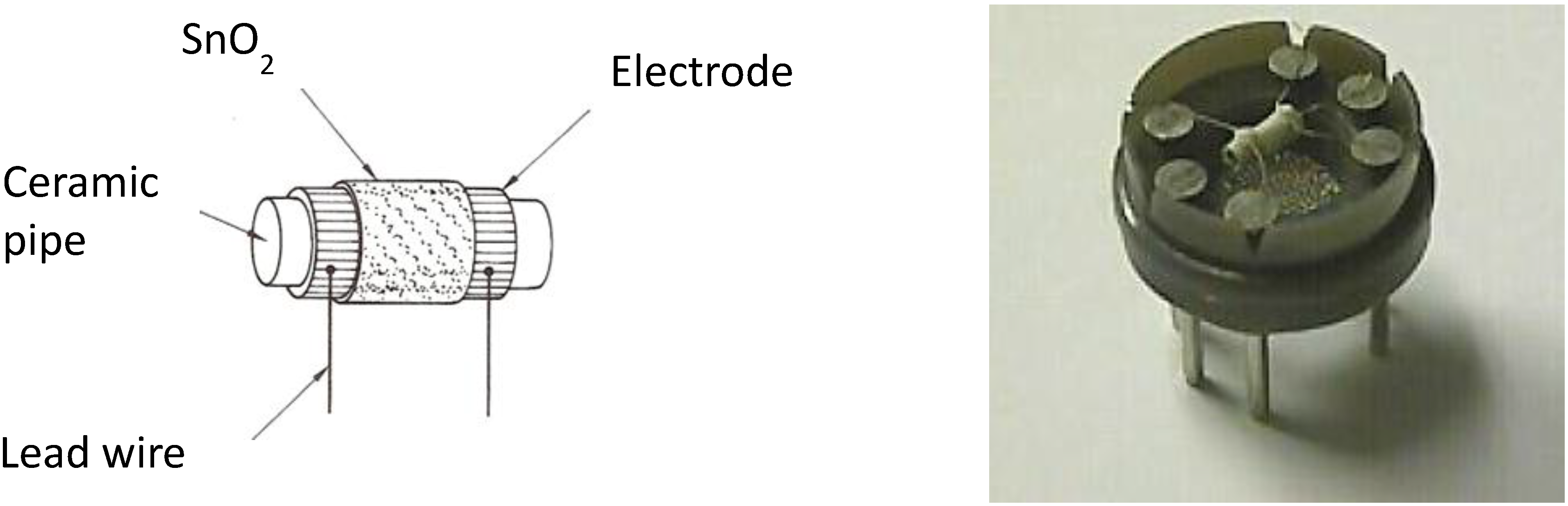
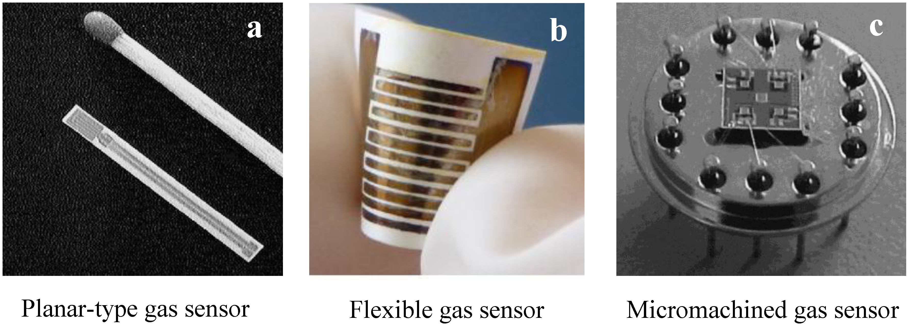
Classical Taguchi sensors have a sensitive material in the form of sintered porous ceramic body (see Figure 1). Other examples of chemoresistive sensors bearing different forms and dimensions are shown in Figure 2.
Figure 1.
Schematization and picture of Taguchi chemoresistive gas sensor.

Figure 2.
Chemoresistive gas sensors with different configurations.

Planar-type gas sensors are constituted of a sensing thick/thin layer deposited by chemical or physical methods onto a ceramic substrate with interdigited electrodes (Figure 2a). The sensing layer can be deposited also on a plastic support, thereby allowing the fabrication of flexible chemoresistive gas sensors (Figure 2b).
Although these sensors are small in size, further miniaturization of sensors is demanded by a variety of applications. In particular, compatibility with integrated circuit (IC) technology is now largely pursued. Fully integrated devices have been fabricated using top-down processes, but the top-down approach typically has the advantage of higher throughput and amenability for large-scale integration. By these techniques, micromachined chemoresistive sensors can be fabricated on a chip substrate, enabling easy interfacing with conventional silicon microelectronics (Figure 2c).
The continual drive towards even finer microstructures will lead to the fabrication of sensing nanodevices. Already now there are existing mature industrial technologies (e.g., technologies based on thin film semiconductors), but long-term stability could be a serious problem for these sensing nanodevices. For example, sensing nanomaterials may be quite unstable under thermal conditions due to their high surface energy leading to severe grain growth, which may result in the degradation of the device performances. Under such operations, the mechanical deterioration of electrodes can also lead to performance degradation due to the possible formation of micro-cracks on the electrode structure.
Therefore, unless there are significant cost and/or performance benefits from using nanosensors, it will be difficult to displace the existing bulk sensor technologies in the near future.
2.2. Sensing Materials
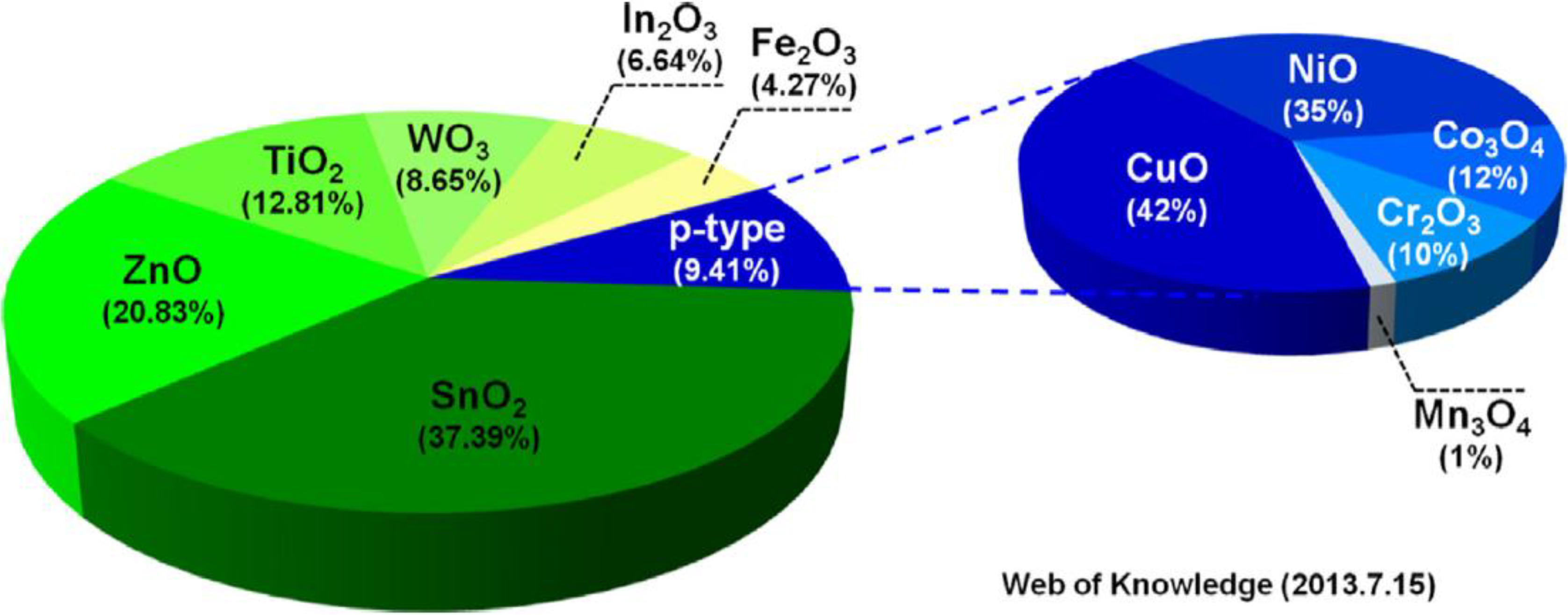
From the first tin dioxide sensor developed in the 1970s for domestic gas alarms, there has been an increase in the demand for high performance solid-state gas sensors. Results of a search study on semiconductor metal oxides used as sensing materials for chemoresistive gas sensors, including both the n-type and p-type oxides, are summarized in the graph shown in Figure 3.
Figure 3.
Studies on n- and p-type oxide semiconductor gas sensors (internet search of Web of Knowledge). Reprinted with permission from [15].
Figure 3.
Studies on n- and p-type oxide semiconductor gas sensors (internet search of Web of Knowledge). Reprinted with permission from [15].

Metal oxides stand out as one of the most common, diverse and, most likely, largest class of materials due to their extensive structural, physical and chemical properties and functionalities. The most common metal oxides utilized as sensing layer in chemoresistive devices are binary oxides such as SnO2, ZnO, TiO2, etc.; however, ternary and more complex oxides are also applied in practical gas sensors [14].
SnO2 is the most extensively studied metal oxide and is widely applied in practical commercial devices. Tin dioxide is a wide-band gap (3.6 eV) semiconductor with interesting electrical properties [20]. Due to its high sensitivities for different gas species, tin oxide-based sensors allow the detection of low concentration levels of gaseous species, though it unfortunately suffers from the lack of selectivity. Nevertheless, strategies devoted to enhance the SnO2-based devices performance (synthesis and treatment conditions, and nano- micro- and nano-structure, addition of dopants) have been extensively studied [21].
Zinc oxide is a II−VI semiconductor showing a wide-band gap (3.37 eV), with the dominant defects identified as O vacancies [22]. ZnO has attracted much attention in the gas-sensing field because of its high mechanical and chemical stability, suitability to doping, non-toxicity and low cost. The sensing property of ZnO is strongly influenced by the microstructural features, such as the grain size, geometry and connectivity between the grains.
Titania is particularly attractive for gas sensors because of its lower cross-sensitivity to humidity than other metal oxides [23]. Among the other applications, TiO2 has been largely investigated as a sensing layer in resistive oxygen gas sensors operating at medium-high temperatures for automotive air/fuel ratio control. At medium temperatures (400–600 °C), oxygen detection is mainly due to reactions that takes place on the surface, whereas at high temperatures (700–1000 °C), oxygen detection is mainly due to diffusion of oxygen ions in the bulk of the material [24].
A lot of factors affect the gas sensor performance of metal oxide chemosensors which, in turn, is determined by the reception and transduction function along with the fabrication procedure [16]. The synthesis procedure, crystal size and shape, the addition of foreign elements with the role of sensitizers or conductivity modifiers are some of the factors influencing the sensor response [17,18,19,20,21,22,23,24,25].
Doping the metal oxide layer with suitable promoters (metal particles, foreign metal oxide, ions) is a common way of enhancing the sensing characteristics of chemoresistive gas sensors. A comprehensive review dealing with all aspects of metal doping can be found in [26]. The modification of the sensing properties of the sensing material by the introduced additives depends on the nature of the latter. For example, Pt is known to promote the gas-sensing reaction by the spill-over of sample gas (chemical sensitization), whereas Pd is known to promote the gas-sensing reaction by electronic interaction between Pd and sensing materials (electronic sensitization) [27].
The grain-size reduction at nanometric level is another of the main factors enhancing the detection properties of metal oxides. It is in fact well recognized that by reducing the particle size of the sensing material in the nanometer range the sensitivity of chemoresistive gas sensors is greatly improved both for the large specific surface offered and for the influence in reducing the surface charge density [21,28,29,30,31,32,33,34,35]. Furthermore, in this size range, a large fraction of the atoms (up to 50%) are present at the surface or the interface region; therefore, the chemical and electronic of nanoparticles are different from those of the bulk, consequently contributing to an increase in the sensing properties.
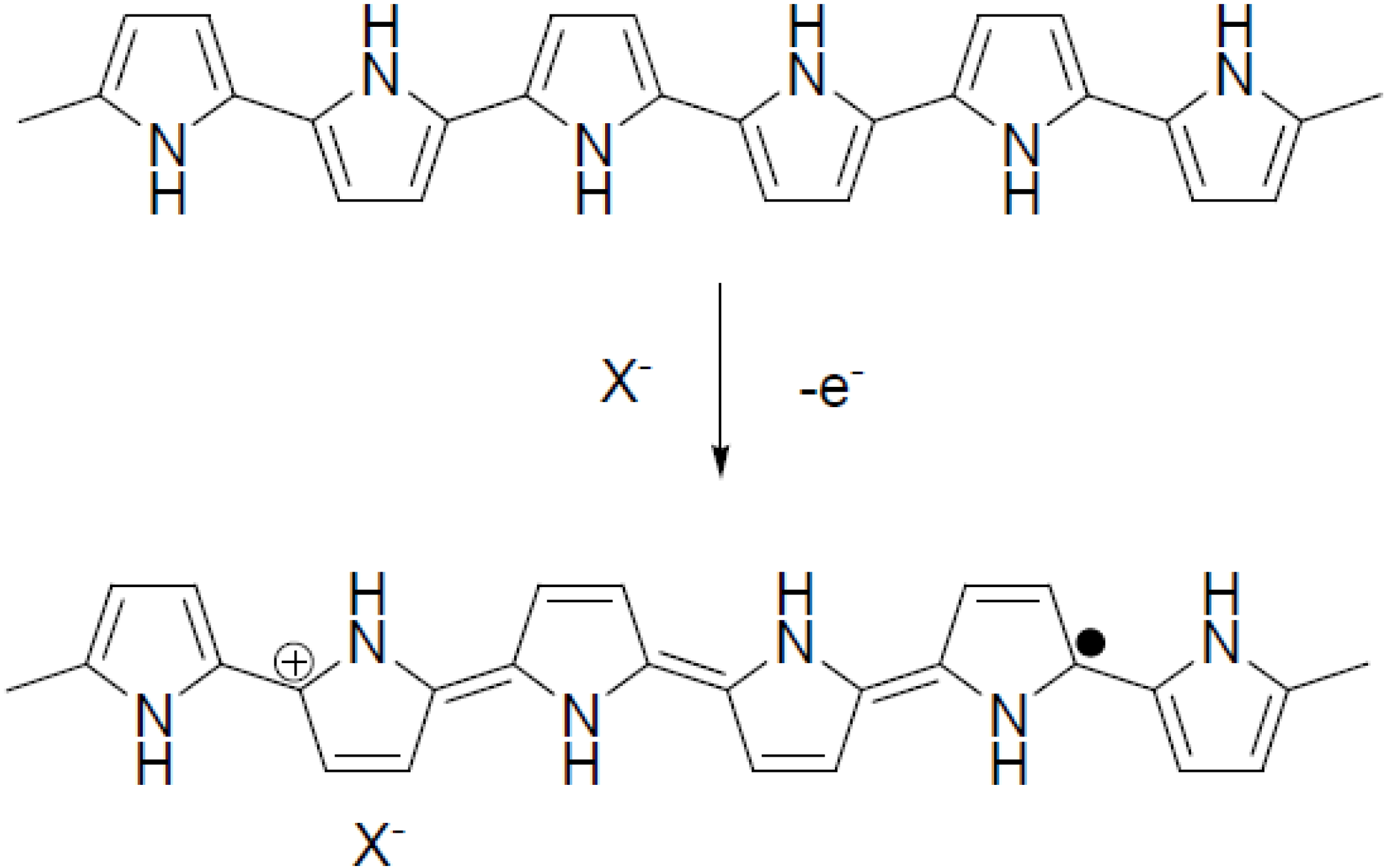
Over the last fifty years, novel sensing materials others than metal oxides have been proposed. In 1983, the gas-sensing properties of conducting polymers were first reported. The sensor involved the use of doped polypyrrole (PPy), functioning as an ammonia sensor [36]. In fact, as the conductivity of the pure conducting polymer is rather low, in order to achieve the high conductivity suitable for sensing applications, a doping process was necessary (Figure 4). A wide variety of polymers of this type is now available, including substituted polypyrroles, polythiophenes, polyindoles, and polyanilines.
Figure 4.
Molecular structure of polypyrrole (PPy) and related doping process.

Organic materials are much more easily modified than inorganic materials with respect to such characteristics as sensitivity, working temperature, and selectivity. Long-term instability is a main drawback of the sensors based on conducting polymers as they are thermally unstable, so it is often impossible to use them at temperatures at which gas-solid interactions proceed rapidly and reversibly.
To fully use all the potential advantages of organic and inorganic materials, hybrid composites have also been introduced as sensing elements for resistive sensors [37]. These hybrid organic/metal oxide composites are not merely the sum of the individual components, but rather new materials with new functionalities and properties. From the viewpoint of structure, organic support can induce the nucleation, growth and formation of fine metal oxide nano-/microstructures with uniform dispersion and controlled morphology, thereby avoiding the agglomeration of metal oxides. If the organic component is a good electrical conductor (e.g., conductive carbon, carbon nanotubes or graphene), the resulting composites can form a perfect integrated structure with a developed electron conductive network and shortened current transport paths, improving the poor electrical properties and charge transfer of pure metal oxides. Significant synergistic effects, such as room-temperature sensing capability when exposed to low-concentration gases such as NO2, H2, and CO, often occur in hybrid composites because of size effects and interfacial interactions in contrast to the high-temperature operation required for metal oxides alone.
The possibility of synthesized materials having dimensions in the order of nanometers has provided enormous advantages for gas sensing because their extremely high surface-to-volume ratio is ideal for gas molecule adsorption. One important example is that of carbon nanotubes (CNTs), which are currently receiving a great deal of interest in gas sensing. Dai et al. first demonstrated the variety that they can offer for practical applications in highly sensitive gas sensors [38]. The high surface-to-volume ratio, high conductivity and mechanical stability make CNTs very attractive for gas-sensing applications. Carbon nanotubes can now be synthesized by different methods in large quantities and with high purity, such as the chemical vapor deposition (CVD) technique, and can be doped with B- and/or N-groups, thus rendering them very sensitive to a wide range of gas vapors [39]. In a similar way, functionalizing the nanotube surface with the polar COOH group attached, the sensors will give stronger responses towards the volatile organic compounds (VOCs) as their absorption efficiency with these volatile organic molecules will be increased due to the dipole-dipole interactions (mainly hydrogen bonding) between the COOH and the polar organic molecules [40].
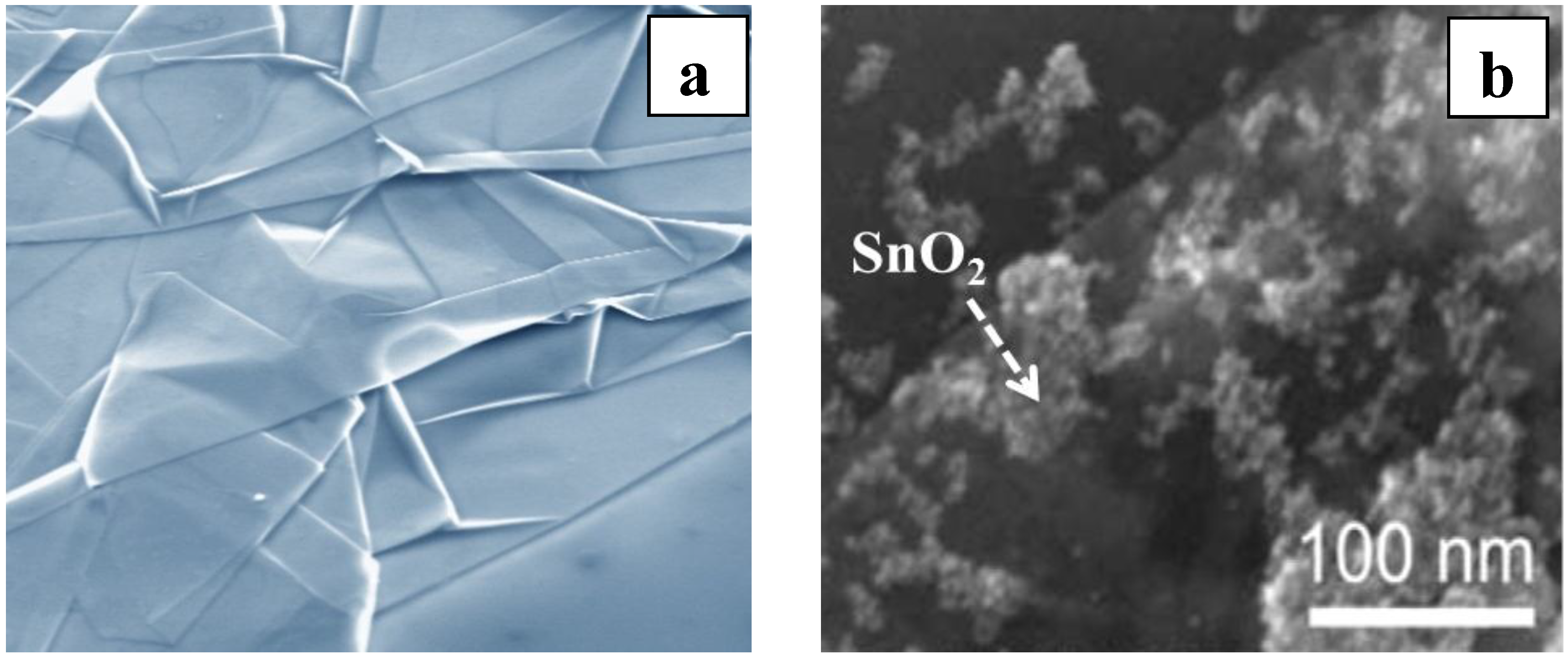
CNTs are also often used as carriers of supported metal oxide particles [41]. CNTs provide high surface area, then help the dispersion of the sensing materials on the nanotube walls (Figure 5a). The better performance of these hybrid sensors are also attributed to the effective electron transfer between the metal oxide particles and the highly conductive carbon nanotube network [42,43,44]. CNTs could also be coated with metal oxides of controlled thickness [45]. By combining the non-aqueous sol-gel route with the atomic layer deposition, metal oxides have been grown from the respective metal alkoxide precursors at low temperatures (Figure 5b). Moreover, the surface reaction leading to the M−O−M bond formation is self-limited and allows then the deposition of films with well-controlled thickness on the internal and external surface of CNTs.
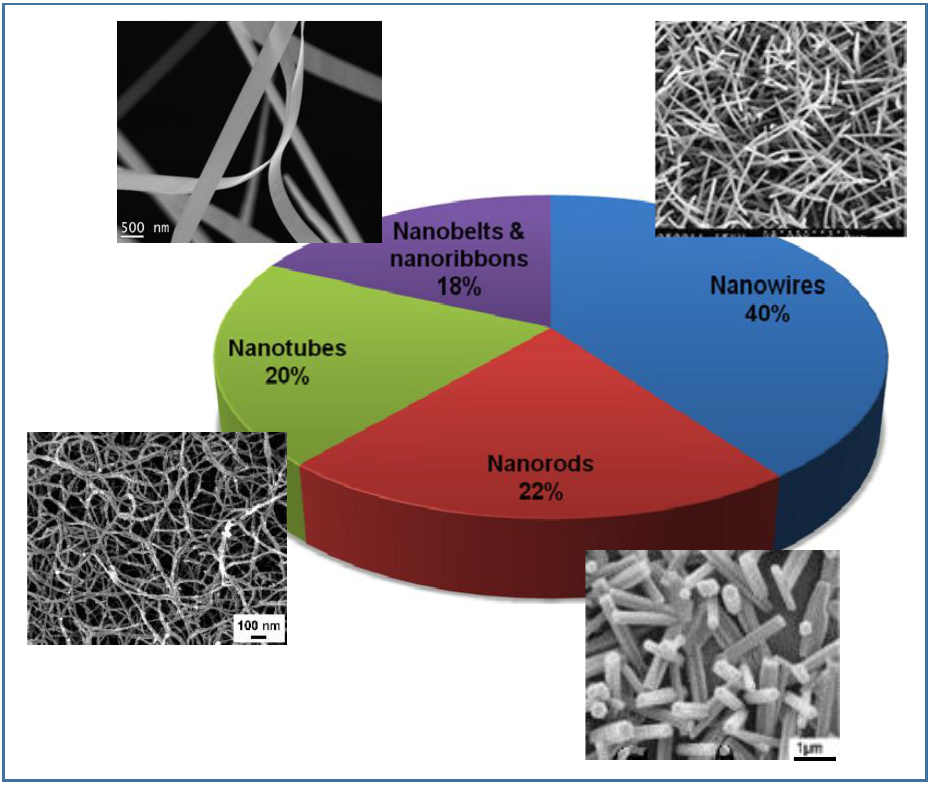
The successful synthesis of nanoparticles, nanowires, nanotubes and other shapes has generated a lot of work to use these nanostructured materials in gas sensing [46,47,48,49,50]. In particular, low-dimensional structures of metal oxides were found to possess characteristics and enhanced gas-sensing properties. In 2002, the Sberveglieri and Yang groups initiated the investigation of gas-sensing properties of one-dimensional nanostructures [51,52]. The shape and morphology of the key one-dimensional nanostructures in chemoresistive sensors are shown in Figure 6.
Figure 5.
SEM images showing metal oxide nanoparticles, visible as white spots, dispersed on CNT: (a) irregularly coated CNT; (b) uniformly coated CNT. Reprinted with permission from [45].
Figure 5.
SEM images showing metal oxide nanoparticles, visible as white spots, dispersed on CNT: (a) irregularly coated CNT; (b) uniformly coated CNT. Reprinted with permission from [45].

Figure 6.
Morphology of the key one-dimensional nanostructures in gas chemiresitors (internet search of Web of Knowledge). Adapted from [53].
Figure 6.
Morphology of the key one-dimensional nanostructures in gas chemiresitors (internet search of Web of Knowledge). Adapted from [53].

Hierarchical and hollow oxide nanostructures are also very promising gas sensor materials due to well-aligned nanoporous structures with less agglomerated configurations. The literature data clearly show that these peculiar nanostructures can increase both the gas response and response speed simultaneously and substantially [54]. This can be explained by the rapid and effective gas diffusion toward the entire sensing surfaces via the highly porous structures.
In 2007, a two-dimensional monolayer of carbon atoms, named graphene, has been identified to be a promising sensing material because it has unique and excellent electrical and mechanical properties [55]. Graphene appears to be more suitable for integration into devices than CNTs because its planar nanostructure makes graphene advantageous for use in standard microfabrication techniques. Furthermore, the sheet structure of graphene (Figure 7a) makes it suitable for depositing and stabilizing small metal and/or metal oxide nanoparticles (Figure 7b), which is of remarkable interest for use in gas sensors.
Figure 7.
(a) Graphene sheets; (b) picture of metal oxide nanoparticles deposited on graphene sheets.
Figure 7.
(a) Graphene sheets; (b) picture of metal oxide nanoparticles deposited on graphene sheets.

2.3. Working Mechanism
Along with the improvement of the characteristics and properties of the devices, a great deal of effort has been also made during these years to improve knowledge of the sensing mechanism and understanding the related processes. The description of mechanisms of chemoresistive sensors based on metal oxides was first depicted through the application of electron theory of chemisorption and catalysis on semiconductors originally formulated by Wolkenstein [56].
Later, Morrison, Yamazoe and Gopel especially contributed to the description of conditions of transport of electric charges through the metal oxide semiconducting layer in the presence of oxygen and reactive gases [57,58,59]. Following these theories, the sensing mechanism of MOS sensors relies on reactions which occur between adsorbed oxygen species and the probed gas on the surface of the sensing layer. Details on this subject can be found in many books and reviews [10,12,60,61]. In first approximation, oxygen adsorbed on the surface of n-type metal oxide semiconductors plays a key role, trapping free electrons because of its high electron affinity, and forming a potential barrier at the grain boundaries. This potential barrier restricts the flow of electrons, causing the electric resistance to increase. When the sensor is exposed to an atmosphere containing reducing gases, e.g., CO, the gas molecules adsorbs on the surface and reacts with active oxygen species, e.g., O−, which liberates free electrons in the bulk. This lowers the potential barrier allowing electrons to flow more easily, thereby reducing the electrical resistance. With oxidizing gases such as NO2 and ozone, the adsorption process increases instead the surface resistance [62]. The converse is true for p-type oxides, where electron exchange due to the gas interaction leads either to a reduction (reducing gas) or an increase (oxidizing gas) in electron holes in the valence band [63]. However, to give a complete description of the gas-sensing mechanism for these sensors, it is necessary to take into account all elementary steps (adsorption, reaction, desorption, etc.) governing surface-gas target interactions leading to charge transfer [64].
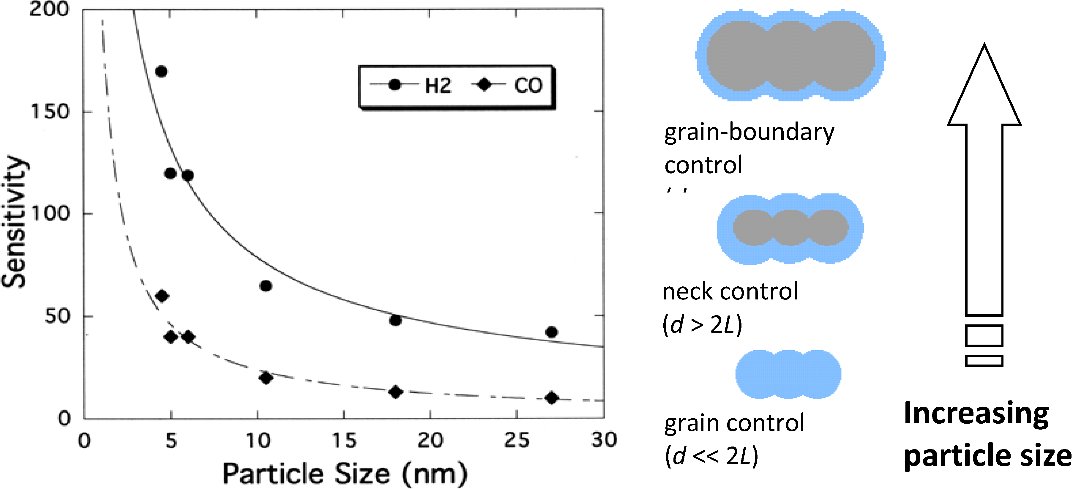
Yamazoe first demonstrated that reduction in crystal size would significantly increase the sensor performance [7]. In particular, the sensitivity of metal oxides is drastically promoted when the crystallite size, D, is in the nanometer range (Figure 8). The sensing properties are partially associated with the depth of the surface space charge region which is affected by the gas adsorption and depend on the particle size. Specifically, the sensor’s response increases significantly if the crystallite size is about twice the adsorption depth, 2L (L is the depth of the space-charge layer), of oxygen adsorbates. This means that the sensor performance improves not only when D decreases, but also if L increases, since a major proportion of material takes place in the reaction of oxygen adsorbates with the target gas even if the grain size is not excessively small. For a typical sensing material, SnO2, with different grain sizes between 5 and 80 nm, simulations showed that the conductivity increases linearly with decreasing trapped charge densities and the sensitivity to the gas-induced variations in the trapped charge density increases too, in agreement with experimental findings [65].
Figure 8.
Sensitivity to H2 and CO of SnO2 vs. particle size and sensing mechanisms associated. Adapted with permission from [7].
Figure 8.
Sensitivity to H2 and CO of SnO2 vs. particle size and sensing mechanisms associated. Adapted with permission from [7].

When dealing with wire with lateral dimensions to the order of hundreds of nanometers, gas adsorption creates a surface depletion layer, consequently reducing the conducting channel thickness [50,66]. The mobility dependence on surface coverage can be neglected because electron diffusion length (about 1 nm) is much shorter than the diameter (tens of nanometers). Electrical transport changes when the thickness of the wire is small like in nano-wires with low lateral dimensions low compared to the Debye length, the space charge region extends through the entire wire cross-section and all electrons are trapped in surface states.
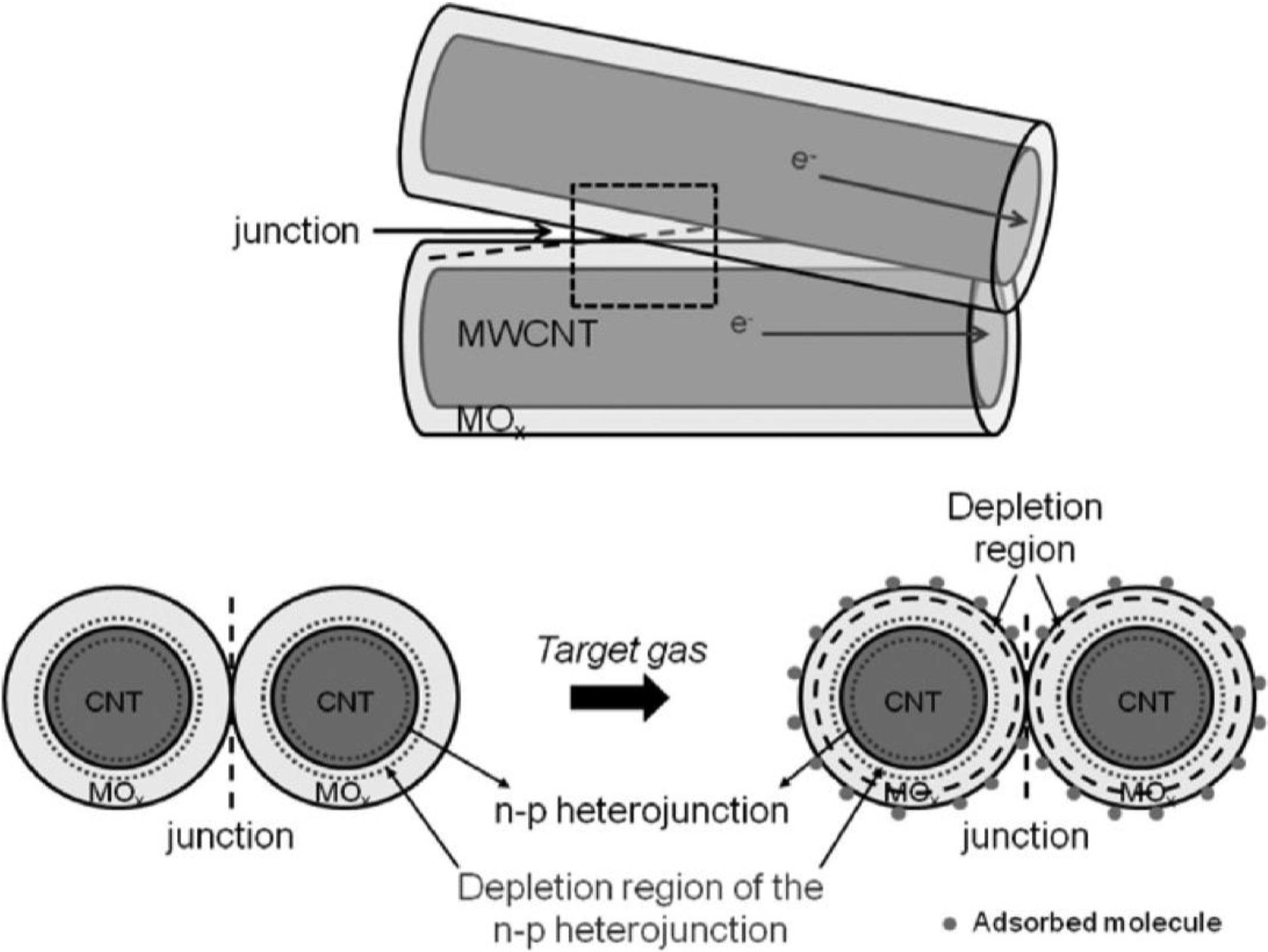
A model of the sensing mechanism of hybrid heterostructures such as metal oxide/CNTs has been attempted. The junctions existing between the nanotubes of the networking at their crossing points (Figure 9), as well as the different depletion regions existing as a function of the presence of the target gas, have been taken into account. Their role in the sensing mechanism has been established by several authors [67,68].
Figure 9.
Schematic illustration of the junctions involved in the sensing mechanism of metal oxide/CNTs. Adapted with permission from [68].
Figure 9.
Schematic illustration of the junctions involved in the sensing mechanism of metal oxide/CNTs. Adapted with permission from [68].

3. Applications of Chemoresistive Gas Sensors
While the previous sections focused on the scientific breakthroughs achieved by constantly pushing the fundaments of sensing materials and devices, focus in the following is addressed towards the applicative aspects of chemoresistive gas sensors.
Rapid, comprehensive, and reliable information regarding the chemical state of a gaseous system is currently indispensable in many high-technology fields. Solid-state gas sensors are thus generating tremendous interest because of their widespread applications in industry, environmental monitoring, space exploration, biomedicine, and pharmaceutics. Generally, basic criteria for these practical gas-sensing devices are: (i) high sensitivity and selectivity; (ii) fast response time and recovery time; (iii) low power consumption; (iv) low operating temperature and temperature independence; (v) high stability.
For most of the practical applications, a relevant problem is not only to estimate the target gas concentration, but also to identify it in the real mixture (outdoor and indoor ambient, exhaust gases, breath). Unfortunately, chemoresistive gas sensors are very sensitive but not selective. Such a task can therefore not be performed by a single sensor. E-nose, an artificial olfactory system consisting of an array of sensors, then needs to be used. Each sensor shows an individual response to all (or to a certain subset) of the target gases which are identified by pattern recognition of the sensor signals, e.g., that developed by Cyrano Sciences is based on the concept of using multiple semi-selective sensors combined with electronic computation, first proposed by Gardner and Bartlett [69].
In the following, some of the most important applicative fields of semiconductor gas sensors are listed.
3.1. Environmental Applications
In environmental applications, field-portable monitors based on chemoresistive sensor devices are particularly suited to comply with the newly reinforced environmental regulations, and give a valuable alternative to conventional analytical techniques; they are accurate but more expensive and time consuming [70]. Metal oxide semiconductor sensors are relatively inexpensive compared to other sensing technologies; they are also robust, lightweight, long lasting and benefit from high material sensitivity and quick response times. These properties could lead to them becoming ever more important tools in environmental monitoring with respect to the other type of sensors. They can be used to measure and monitor trace amounts of environmentally important gases such as carbon monoxide and nitrogen dioxide [71]. Today, it is also highly desirable to develop simple and inexpensive sensors to measure atmospheric carbon dioxide in order to monitor indoor air quality [72].
3.2. Automotive Applications
The ability of chemosensors based on refractory metal oxides to withstand high temperatures, the robust nature, efficient packaging procedures and small size, are strong technical merits for automotive applications. Indeed, usually high temperatures are reached in the exhausts, and sensor devices should operate in the range 600–900 °C in a harsh ambient requiring advanced packaging. Other requirement for these sensors are reaction measurement speed of the order of fraction of seconds and 5–10 year service life. As a result of the introduction of emergent technologies in the automotive industry, new vehicle diagnostic sensors are at present necessary to control motor functioning, monitor a range of emission gases (NO, NO2, CO, CO2, HC, O2, etc.), and detect high pollution levels in the vehicle cabin [73].
Chemoresistive sensors can be used to minimize the emission of CO, hydrocarbons, and nitrogen oxides coming from combustion engines. It is important for the engine to operate with the proper air-to-fuel ratio (A/F) so that combustion parameters are optimized. The first titania gas sensors were developed in the late 1970s and early 1980s. They were primarily used to detect the stoichiometric A/F [74]. In these instances, the sensor resistance increased by orders of magnitude around the stoichiometric A/F, making it a very useful device for these applications.
Chemoresistive sensors will have high importance also in future cars. In fact, CO sensors have been identified as a critical need for proton exchange membrane (PEM) fuel cell systems, which offer a viable approach to improve efficiency of power generation from fossil fuels, while reducing emissions of pollutants and greenhouse gases [75]. The primary uses of such sensors include measurement of the CO content of the reformate gas entering the PEM fuel cell (i.e., for fuel cell protection) and measurement of the CO content of the reformate gas at various catalytic stages of the fuel processor (for fuel processor feedback and control). A further requirement is that these sensors must not exhibit cross-sensitivities to the gaseous components of the reformed gases (e.g., hydrogen, carbon dioxide, and/or humidity) or to other potential contaminants.
3.3. Biomedical Applications
Biomedical uses of chemoresistive gas sensors (e.g., in breath test) require instead high sensitivity to detect very low concentrations of target gases (in the ppt−ppm range), coming from biochemical processes occurring in the human body and used as markers of for several pathologies [76]. Furthermore, the target gas is to be analyzed and quantified in a complex mixture, i.e., in the presence of many other interferent gases and a high humidity content [77]. Such sensors can complement or serve as an alternative to more sophisticated spectrometric systems for breath analysis and speciation, especially for clinical diagnostics and monitoring [78].
3.4. Miscellaneous
During recent years, single or array of metal oxide semiconductor (MOS) sensors have found applications in many other different fields than those listed above, including odor landfill, chemical agent warfare detection, food quality control, etc. [79]. These technologies enable rapid detection and identification of substances based on their chemical profile. They find applications in the monitoring of some medical conditions as well as industrial applications generally related to quality control or contamination detection. A new multi-chamber electronic nose (MCE-nose) which overcomes, to a great extent, one of the major disadvantages of the use of MOS technology for e-noses—the long recovery period needed after each gas exposure that severely restricts its use in applications where the gas concentrations may change rapidly—has been also proposed [80]. It comprises several identical sets of MOS sensors accommodated in separate chambers which alternate between sensing and recovery states, providing, as a whole, a device capable of sensing more quickly changes in chemical concentrations.
4. New Opportunities
Although resistive gas sensors are still commercialized intensively as bulk devices, there is a strong demand for novel, smaller, integrated, high performance and reliable devices for advanced applications. Technological advances will assist gas sensor device scale of economies by exploring more efficient fabrication methods that may include material and component assembly into the final device.
At the material level, technological advances will arise from multidisciplinary contributions, which will hopefully open up new areas of nanoscience research. In the past few years, large efforts have been expended in the development of new synthetic approaches for sensing materials at the nanoscale. Advances in recent activities concerning the synthesis, characterization and properties of novel materials with potential in sensing applications can be found in many reviews [81,82]. Among the obvious challenges are improving reproducibly and control over nanoparticle structure, surface chemistry and dispersion.
Future work will continue to focus also on generating improved component assembly and device fabrication strategies. For small or medium-scale batch production, a hybrid design whereby component parts are created separately for subsequent assembly into a complete system is an attractive option, as it removes many of the restrictions imposed by the need for process compatibility.
Integrated gas sensor with a micro-hotplate (MHP) demonstrates better sensitivity, faster response, and lower power consumption than traditional thick film devices. For the detection of a target gas, a gas-sensitive layer is applied on a suspended micro-hotplate that is mounted on top of a silicon chip. Any gas-induced change of the gas-sensitive layer’s surface potential is detected and digitally processed by the integrated electronics.
Sensor platforms robust enough for integration into standard, industrial weaving processes have been proposed [83]. Such sensors were fabricated on a thin, flexible plastic stripe (e.g., made of Kapton®, DuPont™, Wilmington, De, USA) and woven into a cotton fabric by using a standard weaving machine, to create a smart fabric able to detect ambient gas. The fabrication process is actually very simple and compatible with large-scale roll-to-roll fabrication. Inkjet-printing can be used as an effective, low-cost alternative, suitable for the fabrication of long sensor stripes. Bending tests performed on the devices showed that they can be successfully woven within a cotton fabric using a standard weaving machine without being damaged.
From a processing point of view, employing modern microelectronics technology to manufacture both the sensing element and the signal conditioning circuitry on a single silicon chip, is now possible to make low-power, low-cost smart gas sensors in high volume and this should result in a new generation of miniaturized gas sensors [84]. Full-integration of micro-electronic and micro-mechanical components on a single wafer has been achieved commercially using silicon processing technology. Figure 10 shows a commercial micro electro mechanical system (MEMS) gas sensor for indoor air quality monitoring [85].
Figure 10.
TGS 8100 MEMS gas sensors by FIGARO Eng. Inc., Osaka, Japan.

The sensing element is comprised of a sensing chip and an integrated heater fabricated on a silicon substrate using MEMS technology, and a metal oxide semiconductor layer on the sensing chip. Due to miniaturization of the sensing chip, the sensor requires a heater power consumption of only 15 mW and is suitable for low-power equipment and battery-operated instruments. We expect many areas will benefit from these miniaturized sensors, including transportation (land, sea, air, and space), buildings and facilities (homes, offices, factories), humans (especially for health and medical monitoring) and robotics of all types.
Recent technological advances are quickly changing the landscape of gas sensors. As these devices are becoming smaller in size, require less support infrastructure than currently used equipment, and are capable of operating autonomously, new opportunity for gas sensors could come from their integration into smartphones [86]. Chemical sensors, integrated within smartphones and other wireless and wearable devices, provide a vast array of functionality, from informing people about their environment, air quality and safety, to diagnosing health conditions through breath analysis. For example, background apps on a smartphone (see Figure 11) can monitor CO or CO2 levels and provide Safe/Warning/Alert indication to the user about possible dangerous changes in their environment [87].
Figure 11.
App on smartphone for providing CO or CO2 levels from gas sensors.

Furthermore, monitoring devices can become simpler and cheaper as the computation is pushed to the cloud. This enables users to buy off-the-shelf devices and access customized monitoring applications via cloud-based services.
5. Conclusions
In this paper the historical development of semiconductor gas sensors accomplished during the past five decades has been briefly reviewed. Since early 1970s, after the pioneering work of Seyama and Taguchi, a number of research teams in both academia and industry have been engaged to investigate gas sensing mechanism and propose gas sensor devices featuring a wide offering of functionalities. With the advent of the latest technological breakthroughs, recent progress in gas sensor devices has been stimulated by inter-disciplinary perspectives at the intersection of materials science, microelectronics, nanotechnology and signal processing/pattern recognition in an attempt to overcome limitations of early systems. The effect of microstructure, size feature of the material, the advantages of novel nano-structured materials, have been widely pursued to improve the sensors’ performance as well as to reduce their power consumption. With time, sensors migrated to process control market, then industrial controls, automotive and medical markets. Further, as embedded system technologies continues to growth at very fast rates offering great functionality at lower costs, efforts in gas sensing area seek for system solutions based on miniaturized smart sensors. Taking this into account, new generation of semiconductor gas sensors are now appearing in cloth fabrics, smart phones, media tablets, etc., and in the near future will permeate the lives of consumers in ways unimaginable 50 years ago.
Conflicts of Interest
The author declares no conflict of interest.
References
- Seiyama, T.; Kato, A. A new detector for gaseous components using semiconductor thin film. Anal. Chem. 1962, 34, 1502–1503. [Google Scholar] [CrossRef]
- Brattain, W.H.; Bardeen, J. Surface properties of germanium. Bell Syst. Tech. J. 1952, 32, 1–41. [Google Scholar] [CrossRef]
- Heiland, G. Zum einfluss von wasserstoff auf die elektrische leitfähigkeit von ZnO-kristallen. Z. Phys. 1954, 138, 459–464. [Google Scholar] [CrossRef]
- Shaver, P.J. Activated tungsten oxide gas detectors. Appl. Phys. Lett. 1967, 11, 255–257. [Google Scholar] [CrossRef]
- Taguchi, N. Gas Detecting Devices. U.S. Patent 3,631,436, 28 December 1971. [Google Scholar]
- Seiyama, T. Chemical sensors—Current status and future outlook. In Chemical Sensor Technology; Seiyama, T., Ed.; Elsevier: Amsterdam, The Netherlands, 1988; Volume 1. [Google Scholar]
- Yamazoe, N. New approaches for improving semiconductor gas sensors. Sens. Actuators B Chem. 1991, 5, 7–19. [Google Scholar] [CrossRef]
- Shimizu, Y.; Egashira, M. Basic aspects and challenges of semiconductor gas sensors. MRS Bull. 1999, 24, 18–24. [Google Scholar] [CrossRef]
- Yamazoe, N. Toward innovations of gas sensor technology. Sens. Actuators B Chem. 2005, 108, 2–14. [Google Scholar] [CrossRef]
- Williams, D.E. Solid State Gas Sensors; Moseley, P.T., Tofield, B.C., Eds.; Adam Hilger: Bristol, UK, 1987. [Google Scholar]
- Gerblinger, J.; Hardtl, K.H.; Meixner, H.; Aigner, R. High-Temperature Microsensors. In Sensors Set: A Comprehensive Survey; Gopel, W., Ed.; VCH-Verlag: Weinheim, Germany, 1995; p. 181. [Google Scholar]
- Sberveglieri, G. Gas Sensors; Kluwer Academic Publishing: Berlin, Germany, 1992. [Google Scholar]
- Capone, S.; Siciliano, P. Encyclopedia of Nanoscience and Nanotechnology; Nalwa, H.S., Ed.; American Scientific Publishers: Valencia, CA, USA, 2004; Volume 3, p. 769. [Google Scholar]
- Gurlo, A.; Bârsan, N.; Weimar, U. Gas sensors based on semiconductiong metal oxides. In Metal Oxides: Chemistry and Applications; Fierro, J.L.G., Ed.; CRC Press: Boca Raton, FL, USA, 2006; p. 683. [Google Scholar]
- Kim, H.-J.; Lee, J.-H. Highly sensitive and selective gas sensors using p-type oxide semiconductors: Overview. Sens. Actuators B Chem. 2014, 192, 607–627. [Google Scholar] [CrossRef]
- Yamazoe, N.; Shimanoe, K. Receptor function and response of semiconductor gas sensor. J. Sens. 2009, 2009, 875704. [Google Scholar] [CrossRef]
- Aleixandre, M.; Gerboles, M. Review of small commercial sensors for indicative monitoring of ambient gas. Chem. Eng. Trans. 2012, 30, 169–174. [Google Scholar]
- Huang, X.-J.; Choi, Y.-K. Chemical sensors based on nanostructured materials. Sens. Actuators B Chem. 2007, 122, 659–671. [Google Scholar] [CrossRef]
- Jimenez-Cadena, G.; Riu, J.; Xavier Rius, F. Gas sensors based on nanostructured materials. Analyst 2007, 132, 1083–1099. [Google Scholar] [CrossRef]
- Ogawa, H.; Nishikawa, M.; Abe, A. Hall measurement studies and an electrical conduction model of tin oxide ultrafine particle films. J. Appl. Phys. 1982, 53, 4448–4455. [Google Scholar] [CrossRef]
- Korotcenkov, G. Gas response control through structural and chemical modification of metal oxide films: State of the art and approaches. Sens. Actuators B Chem. 2005, 107, 209–232. [Google Scholar] [CrossRef]
- Mahmood, M.R.; Soga, T.; Mamat, M.H.; Khusaimi, Z.; Nor, A.M. A Review on zinc oxide nanostructures: Doping and gas sensing. Adv. Mater. Res. 2013, 667, 329–332. [Google Scholar] [CrossRef]
- Tricoli, A.; Righettoni, M.; Pratsinis, S.E. Minimal cross-sensitivity to humidity during ethanol detection by SnO2-TiO2 solid solutions. Nanotechnology 2009, 20, 315502. [Google Scholar] [CrossRef] [PubMed]
- Ramamoorthy, R.; Dutta, P.K.; Akbar, S.A. Oxygen sensors: Materials, methods, designs and applications. J. Mater. Sci. 2003, 38, 4271–4282. [Google Scholar] [CrossRef]
- Malagù, C.; Guidi, V.; Carotta, M.C.; Martinelli, G. Unpinning of Fermi level in nanocrystalline semiconductors. Appl. Phys. Lett. 2004, 84, 4158–4160. [Google Scholar]
- Neri, G. Encyclopedia of Sensors; Grimes, C.A., Dickey, E.C., Pishko, M.V., Eds.; American Scientific Publishers: Valencia, CA, USA, 2006; Volume 6, p. 1. [Google Scholar]
- Cabot, A.; Arbiol, J.; Morante, J.R.; Weimar, U.; Barsan, N.; Gopel, W. Analysis of the noble metal catalytic additives introduced by impregnation of as obtained SnO2 sol-gel nanocrystals for gas sensors. Sens. Actuators B Chem. 2000, 70, 87–100. [Google Scholar] [CrossRef]
- Baraton, M.-I.; Merhari, L. Influence of the particle size on the surface reactivity and gas sensing properties of SnO2 nanopowders. Mater. Trans. 2001, 42, 1616–1622. [Google Scholar] [CrossRef]
- Xu, C.; Tamaki, J.; Miura, N.; Yamazoe, N. Grain size effects on gas sensitivity of porous SnO2-based elements. Sens. Actuators B Chem. 1991, 3, 147–155. [Google Scholar] [CrossRef]
- Dolbec, R.; el Khakani, M.A.; Serventi, A.M.; Saint-Jacques, R.G. Influence of the nanostructural characteristics on the gas sensing properties of pulsed laser deposited tin oxide thin films. Sens. Actuators B Chem. 2003, 93, 566–571. [Google Scholar] [CrossRef]
- Gurlo, A.; Ivanovskaya, M.; Barsan, N.; Schweizer-Berberich, M.; Weimar, U.; Gopel, W.; Dieguez, A. Grain size control in nanocrystalline In2O3 semiconductor gas sensors. Sens. Actuators B Chem. 1997, 44, 327–333. [Google Scholar] [CrossRef]
- Ansari, S.G.; Boroojerdian, P.; Sainkar, S.R.; Karekar, R.N.; Aiyer, R.C.; Kulkarni, S.K. Grain size effects on H2 gas sensitivity of thick film resistor using SnO2 nanoparticles. Thin Solid Films 1997, 295, 271–276. [Google Scholar] [CrossRef]
- Dieguez, A.; Romano-Rodriguez, A.; Morante, J.R.; Weimar, U.; Schweizer-Berberich, M.; Gopel, W. Morphological analysis of nanocrystalline SnO2 for gas sensor applications. Sens. Actuators B Chem. 1996, 31, 1–8. [Google Scholar] [CrossRef]
- Korotcenkov, G. The role of morphology and crystallographic structure of metal oxides in response of conductometric-type gas sensors. Mater. Sci. Eng. R 2008, 61, 1–39. [Google Scholar] [CrossRef]
- Rothschild, A.; Komem, Y. Metal oxide gas sensors with nanosized grains. J. Electroceram. 2004, 13, 697–701. [Google Scholar] [CrossRef]
- Nylander, C.; Armgarth, M.; Lundstrom, L. An ammonia detector based on a conducting polymer. Anal. Chem. Symp. Ser. 1983, 17, 203–207. [Google Scholar]
- Jiang, T.; Wang, Z.; Li, Z.; Wang, W.; Xu, X.; Liu, X.; Wang, J.; Wang, C. Synergic effect within n-type inorganic–p-type organic nano-hybrids in gas sensors. J. Mater. Chem. C 2013, 1, 3017–3025. [Google Scholar] [CrossRef]
- Kong, J.; Franklin, N.R.; Zhou, C.; Chapline, M.G.; Peng, S.; Cho, K.; Dai, H. Nanotube molecular wires as chemical sensors. Science 2000, 287, 622–625. [Google Scholar] [CrossRef] [PubMed]
- Peng, S.; Cho, K. Ab initio study of doped carbon nanotube sensors. Nano Lett. 2003, 3, 513–517. [Google Scholar] [CrossRef]
- Sin, M.L.Y.; Chow, G.C.T.; Wong, G.M.K.; Li, W.J.; Leong, P.H.W.; Wong, K.W. Ultralow-power alcohol vapor sensors using chemically functionalized multiwalled carbon nanotubes. IEEE Trans. Nanotechnol. 2007, 6, 571–577. [Google Scholar] [CrossRef]
- Sun, Y.P.; Fu, K.F.; Lin, Y.; Huang, W.J. Functionalized carbon nanotubes: Properties and applications. Acc. Chem. Res. 2002, 35, 1096–1104. [Google Scholar] [CrossRef] [PubMed]
- Lu, G.; Ocola, L.E.; Chen, J. Room-temperature gas sensing based on electron transfer between discrete tin oxide nanocrystals and multiwalled carbon nanotubes. Adv. Mater. 2009, 21, 1–5. [Google Scholar]
- Sun, Y.-F.; Liu, S.-B.; Meng, F.-L.; Liu, J.-Y.; Jin, Z.; Kong, L.-T.; Liu, J.-H. Metal oxide nanostructures and their gas sensing properties: A review. Sensors 2012, 12, 2610–2631. [Google Scholar] [CrossRef] [PubMed]
- Willinger, M.G.; Neri, G.; Rauwel, E.; Bonavita, A.; Micali, G.; Pinna, N. Vanadium oxide sensing layer grown on carbon nanotubes by a new atomic layer deposition process. Nano Lett. 2008, 8, 4201–4204. [Google Scholar] [CrossRef] [PubMed]
- Marichy, C.; Pinna, N. Carbon-nanostructures coated/decorated by atomic layer deposition: Growth and applications. Coord. Chem. Rev. 2013, 257, 3232–3253. [Google Scholar] [CrossRef]
- Lu, J.G.; Chang, P.; Fan, Z. Quasi-one-dimensional metal oxide materials—Synthesis, properties and applications. Mater. Sci. Eng. R 2006, 52, 49–91. [Google Scholar] [CrossRef]
- Pan, Z.W.; Dai, Z.R.; Wang, Z.L. Nanobelts of semiconducting oxides. Science 2001, 291, 1947–1949. [Google Scholar] [CrossRef] [PubMed]
- Li, C.; Zhang, D.; Liu, X.; Han, S.; Tang, T.; Han, J.; Zhou, C. In2O3 nanowires as chemical sensors. Appl. Phys. Lett. 2003, 82, 1613–1615. [Google Scholar] [CrossRef]
- Cao, G. Nanostructures and Nanomaterials; IC Press: London, UK, 2004. [Google Scholar]
- Comini, E. Metal oxide nano-crystals for gas sensing. Anal. Chim. Acta 2006, 568, 28–40. [Google Scholar] [CrossRef] [PubMed]
- Comini, E.; Faglia, G.; Sberveglieri, G. Stable and highly sensitive gas sensors based on semiconducting oxide nanobelts. Appl. Phys. Lett. 2002, 81, 1869–1871. [Google Scholar] [CrossRef]
- Law, M.; Kind, H.; Messer, B.; Kim, F.; Yang, P.D. Photochemical sensing of NO2 with SnO2 nanoribbon nanosensors at room temperature. Angew. Chem. Int. Ed. 2002, 41, 2405–2408. [Google Scholar] [CrossRef]
- Choi, K.J.; Jang, H.W. One-dimensional oxide nanostructures as gas-sensing materials: Review and issues. Sensors 2010, 10, 4083–4099. [Google Scholar] [CrossRef] [PubMed]
- Lee, J.-H. Gas sensors using hierarchical and hollow oxide nanostructures: Overview. Sens. Actuators B Chem. 2009, 140, 319–336. [Google Scholar] [CrossRef]
- Schedin, F.; Geim, A.K.; Morozov, S.V.; Hill, E.W.; Blake, P.; Katsnelson, M.I.; Novoselov, K.S. Detection of individual gas molecules adsorbed on graphene. Nat. Mater. 2007, 6, 652–655. [Google Scholar] [CrossRef] [PubMed] [Green Version]
- Wolkenstein, F.F. Effect of ionizing radiation on the adsorptive and catalytic properties of semiconductors. Discuss. Faraday Soc. 1961, 31, 209–218. [Google Scholar] [CrossRef]
- Morrison, R.S. Semiconductor gas sensors. Sens. Actuators 1982, 2, 329–341. [Google Scholar] [CrossRef]
- Yamazoe, N.; Kurokawa, Y.; Seiyama, T. Effects of additives on semiconductor gas sensors. Sens. Actuators B Chem. 1983, 4, 283–289. [Google Scholar] [CrossRef]
- Gopel, W.; Schierbaum, K. SnO2 sensors: Current status and future prospects. Sens. Actuators B Chem. 1995, 26/27, 1–12. [Google Scholar] [CrossRef]
- Azad, A.M.; Akbar, S.A.; Mhaisalkar, S.G.; Birkefeld, L.D.; Goto, K.S. Solid-State Gas Sensors: A Review. J. Electrochem. Soc. 1992, 139, 3690–3704. [Google Scholar] [CrossRef]
- Barsan, N.; Schweizer-Berberich, M.; Göpel, W. Fundamental and practical aspects in the design of nanoscaled SnO2 gas sensors: A status report. Fresenius. J. Anal. Chem. 1999, 365, 287–304. [Google Scholar] [CrossRef]
- Leblanc, E.; Perier-Camby, L.; Thomas, G.; Gibert, R.; Primet, M.; Gelin, P. NOx adsorption onto dehydroxylated or hydroxylated tin dioxide surface. Application to SnO2-based sensors. Sens. Actuators B Chem. 2000, 62, 67–72. [Google Scholar] [CrossRef]
- Li, Y.; Wlodarski, W.; Galatsis, K.; Moslih, S.H.; Cole, J.; Russo, S.; Rockelmann, N. Gas sensing properties of p-type semiconducting Cr-doped TiO2 thin films. Sens. Actuators B Chem. 2002, 83, 160–163. [Google Scholar] [CrossRef]
- Yamazoe, N.; Shimanoe, K. Theory of power laws for semiconductor gas sensors. Sens. Actuators B Chem. 2008, 128, 566–573. [Google Scholar] [CrossRef]
- Rothschild, A.; Komem, Y. The effect of grain size on the sensitivity of nanocrystalline metal-oxide gas sensors. J. Appl. Phys. 2004, 95, 6374–6380. [Google Scholar] [CrossRef]
- Chen, X.; Wong, C.K.Y.; Yuan, C.A.; Zhang, G. Nanowire-Based Gas Sensors. Sens. Actuators B Chem. 2013, 177, 178–195. [Google Scholar] [CrossRef]
- Wei, B.-Y.; Hsu, M.-C.; Su, P.-G.; Lin, H.-M.; Wu, R.-J.; Lai, H.-J. A novel SnO2 gas sensor doped with carbon nanotubes operating at room temperature. Sens. Actuators B Chem. 2004, 101, 81–89. [Google Scholar] [CrossRef]
- Marichy, C.; Russo, P.A.; Latino, M.; Tessonnier, J.-P.; Willinger, M.-G.; Donato, N.; Neri, G.; Pinna, N. Tin dioxide-carbon heterostructures applied to gas sensing: Structure-dependent properties and general sensing mechanism. J. Phys. Chem. C 2013, 117, 19729–19739. [Google Scholar]
- Wilson, A.D.; Baietto, M. Applications and advances in electronic-nose technologies. Sensors 2009, 9, 5099–5148. [Google Scholar] [CrossRef] [PubMed]
- Lee, D.-D.; Lee, A.-S. Environmental gas sensors. IEEE Sens. J. 2001, 1, 214–224. [Google Scholar] [CrossRef]
- Fine, G.F.; Cavanagh, L.M.; Afonja, A.; Binions, R. Metal oxide semi-conductor gas sensors in environmental monitoring. Sensors 2010, 10, 5469–5502. [Google Scholar] [CrossRef] [PubMed]
- Marsal, A.; Dezanneau, G.; Cornet, A.; Morante, J.R. A new CO2 gas sensing material. Sens. Actuators B Chem. 2003, 95, 266–270. [Google Scholar] [CrossRef]
- Pijolat, C.; Pupier, C.; Sauvan, M.; Tournier, G.; Lalauze, R. Gas detection for automotive pollution control. Sens. Actuators B Chem. 1999, 59, 195–202. [Google Scholar] [CrossRef]
- Cederquist, A.; Gibbons, E.; Meitzler, A. Characterization of Zirconia and Titania Engine Exhaust Gas Sensors for Air/Fuel Feedback Control Systems. SAE Tech. Paper 1976. [Google Scholar] [CrossRef]
- Holt, C.T.; Azad, A.-M.; Swartz, S.L.; Rao, R.R.; Dutta, P.K. Carbon monoxide sensor for PEM fuel cell systems. Sens. Actuators B Chem. 2002, 87, 414–420. [Google Scholar] [CrossRef]
- D’Amico, A.; di Natale, C.; Paolesse, R.; Macagnano, A.; Martinelli, E.; Pennazza, G.; Santonico, M.; Bernabei, M.; Roscioni, C.; Galluccio, G.; et al. Olfactory systems for medical applications. Sens. Actuators B Chem. 2008, 130, 458–465. [Google Scholar] [CrossRef]
- Disease Markers in Exhaled Breath; Marczin, N.; Kharitonov, S.A.; Yacoub, M.H.; Barnes, P.J. (Eds.) Marcel Dekker: New York, NY, USA, 2002.
- Righettoni, M.; Amann, A.; Pratsinis, S.E. Breath analysis by nanostructured metal oxides as chemo-resistive gas sensors. Mater. Today 2014. [Google Scholar] [CrossRef]
- Casalinuovo, I.; Pierro, D. Application of electronic noses for disease diagnosis and food spoilage detection. Sensors 2006, 6, 1428–1439. [Google Scholar] [CrossRef]
- Gonzalez-Jimenez, J.; Monroy, J.G.; Blanco, J.L. The multi-chamber electronic nose—An improved olfaction sensor for mobile robotics. Sensors 2011, 11, 6145–6164. [Google Scholar] [CrossRef] [PubMed]
- Neri, G. Better sensors through chemistry: Some selected examples. Lect. Notes Electr. Eng. 2011, 91, 19–30. [Google Scholar]
- Carbone, L.; Cozzoli, P.D. Colloidal heterostructured nanocrystals: Synthesis and growth mechanisms. Nano Today 2010, 5, 449–493. [Google Scholar] [CrossRef]
- Ataman, C.; Kinkeldei, T.; Mattana, G.; Vásquez Quintero, A.; Molina-Lopez, F.; Courbat, J.; Cherenack, K.; Briand, D.; Tröster, G.; de Rooij, N.F. A robust platform for textile integrated gas sensors. Sens. Actuators B Chem. 2013, 177, 1053–1061. [Google Scholar] [CrossRef]
- Gardner, J.W.; Guha, P.K.; Udrea, F.; Covington, J.A. CMOS interfacing for integrated gas sensors: A review. IEEE Sens. J. 2010, 10, 1833–1848. [Google Scholar] [CrossRef]
- MEMS Technical Data. Available online: http://www.memsgassensor.com (accessed on 28 February 2014).
- Oletic, D.; Bilas, V. Empowering smartphone users with sensor node for air quality measurement. J. Phys. Conf. Ser. 2013, 450, 012028. [Google Scholar] [CrossRef]
- Sensorcon. Available online: http://sensorcon.com (accessed on 10 December 2014).
© 2015 by the authors; licensee MDPI, Basel, Switzerland. This article is an open access article distributed under the terms and conditions of the Creative Commons Attribution license (http://creativecommons.org/licenses/by/4.0/).
Share and Cite
MDPI and ACS Style
Neri, G. First Fifty Years of Chemoresistive Gas Sensors. Chemosensors 2015, 3, 1-20. https://0-doi-org.brum.beds.ac.uk/10.3390/chemosensors3010001
AMA Style
Neri G. First Fifty Years of Chemoresistive Gas Sensors. Chemosensors. 2015; 3(1):1-20. https://0-doi-org.brum.beds.ac.uk/10.3390/chemosensors3010001
Chicago/Turabian StyleNeri, Giovanni. 2015. "First Fifty Years of Chemoresistive Gas Sensors" Chemosensors 3, no. 1: 1-20. https://0-doi-org.brum.beds.ac.uk/10.3390/chemosensors3010001