Article

Improved Synthesis of ZnO Nanowalls: Effects of Chemical Bath Deposition Time and Annealing Temperature

1
Dipartimento di Fisica e Astronomia “Ettore Majorana”, Università Degli Studi di Catania, via S. Sofia 64, 95123 Catania, Italy
2
MATIS CNR-IMM, via S. Sofia 64, 95123 Catania, Italy
3
BRIT (Bio-nanotechResearchInnovationTower), Università degli Studi di Catania, via S. Sofia 89, 95123 Catania, Italy
*
Author to whom correspondence should be addressed.
Submission received: 18 February 2019 / Revised: 26 March 2019 / Accepted: 27 March 2019 / Published: 1 April 2019
(This article belongs to the Special Issue Nanotechnology Efforts for Chemical Sensors)

Abstract

:
Zinc Oxide (ZnO) nanowalls (NWLs) are interesting nanostructures for sensing application. In order to push towards the realization of room-temperature operating sensors, a detailed investigation of the synthesis effect on the electrical and optical properties is needed. This work focuses on the low-cost synthesis of ZnO NWLs by means of chemical bath deposition (growth time of 5, 60, and 120 min) followed by annealing in inert ambient (temperature of 100, 200, and 300 °C). The as-grown NWLs show a typical intertwined network of vertical sheets whose features (thickness and height) stabilize after 60 min growth. During thermal annealing, NWLs are converted into ZnO. The electric transport across the ZnO NWL network radically changes after annealing. A higher resistivity was observed for longer deposition times and for higher annealing temperatures, at which the photoluminescence spectra resemble those obtained for ZnO material. A longer deposition time allows for a better transformation to ZnO during the annealing, thanks to the presence of ZnO seeds just after the growth. These findings can have a significant role in promoting the realization of room-temperature operating sensors based on ZnO NWLs.

1. Introduction

Zinc Oxide (ZnO) nanostructures, thanks to biocompatibility, non-toxicity, low cost, earth abundance, and chemical and thermal stability, have attracted a large industrial and academic interest for applications in gas sensing [1,2,3,4,5]. In particular, Seyama et al. demonstrated that ZnO thin film as a sensing layer for a gas sensor is able to detect gaseous species such as propane at very low concentrations [6]. Indeed, research in the field of gas sensing has looked at ZnO nanostructures because they combine the excellent properties of zinc oxide with their high surface-to-volume ratio, allowing for the realization of gas sensors with very high sensitivity and selectivity [4,7,8].
Generally, ZnO gas sensors need elevated operating temperatures (300–500 °C) to enable a reliable gas detection. Indeed, temperature controls the reaction kinetics, conductivity, and electron mobility [7]. However, the usage of high temperatures increases the device energy consumption and limits its application for the detection of flammable and explosive gaseous species. Thus, the realization of gas sensors operating at room temperature is very challenging.
In this scenario, the use of UV light represents a promising route since UV light can induce gas desorption kinetics similar to what happens at high temperatures. Moreover, UV photons generate electron-hole pairs in ZnO, and the photo-induced carriers can interact with adsorbed gaseous species [7,9]. This can allow for the realization of gas sensors UV-activated at room temperature using ZnO nanostructures like nanosheets (hexagonal foils with thickness of about 100 nm and length of few micrometers), nanorods (parallelepipeds with a hexagonal base with a diameter greater than 50 nm and length of about 1.5 µm), and nano and microwires (cylindrical structures with length of about 10 µm and diameter of few nanometers and micrometers, respectively) [9,10,11,12,13,14].
Among the ZnO nanostructures, ZnO nanowalls (NWLs), i.e., 2D layers of few atomic planes grown perpendicularly to the substrate, are characterized by a huge surface-to-volume ratio and extremely thin wall thickness. Thus, these nanostructures, thanks to their large specific area and numerous active sites for gas adsorption [8], can further improve the interaction with the gas target in order to obtain extremely efficient gas sensors [8,15]. It is also worth noting that ZnO nanowalls can be realized with a simple and low-cost method, like chemical bath deposition (CBD), that does not require low pressures or high temperatures [16]. Recent studies on gas sensors based on ZnO nanowalls already showed the potential of these structures to selectively detect CO and NO2 with a limit of detection of 50 ppb and a working temperature between 250 and 400 °C [15]. Given the excellent properties of ZnO NWLs for gas sensing at high temperatures, a detailed study of the electrical and optical properties can open the route towards room temperature gas sensing.
In this work, the morphological, optical, and electrical properties of ZnO nanowalls, synthesized by CBD, were deeply investigated. In particular, the opto-electrical properties were analyzed as a function of the growth time and post-growth annealing temperature. This strategy can be very promising because it does not require alteration of the nanostructures by means of doping or surface functionalization, which can compromise the versatility of the sensor [7].

2. Materials and Methods

2.1. ZnO Nanowalls Synthesis and Thermal Treatment

The synthesis of ZnO nanowalls was performed on a SiO2/Si substrate by means of chemical bath deposition. For this scope, a catalytic thin layer of aluminum (about 65 nm thick) was deposited by magnetron sputtering (Quorum Q300T D) on the substrate at the following condition: Sputter current of 100 mA and chamber pressure of 10−3 mbar in Ar atmosphere at room temperature. The Al thickness was optimized in order to allow the NWLs formation and to avoid that Al remains under the NWLs network after the growth. The ZnO NWLs growth solution was prepared by mixing in a beaker the following components:
  • 2.94 g of zinc nitrate hexahydrate (ZN, Zn(NO3)2·6H2O);
  • 1.4 g of hexamethylenetetramine (HTMA, (CH2)6N4);
  • 400 mL of deionized water (DI, MilliQ, 18.2 MΩ·cm).
The growth solution was mixed by a magnetic stirrer for 10 min and then heated at 90 °C in a boiling water bath for 10 min. Then, pieces of Al/SiO2/Si (1 cm × 1 cm) were vertically immersed in the growth solution held at 90 °C for 5, 60, and 120 min. More details on the growth of ZnO NWLs with this method can be found in Reference [16]. After the synthesis, the samples were rinsed with DI water, sonicated for 1 min, and annealed in nitrogen atmosphere in a horizontal furnace in the temperature range 100–300 °C for 60 min.

2.2. ZnO Nanowalls Characterization

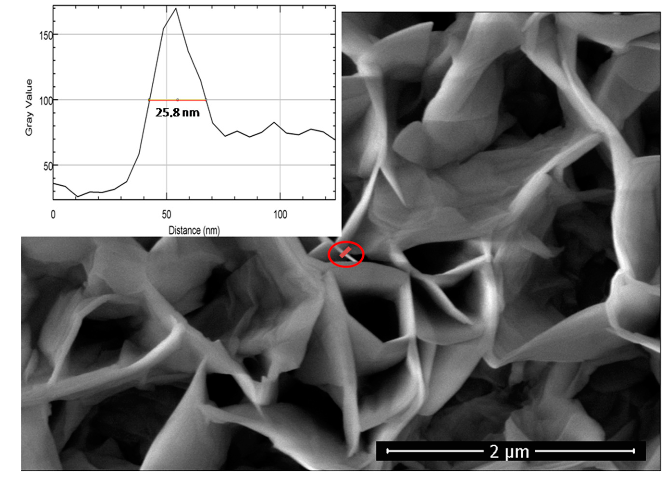
The morphological characterization of the deposited nanomaterials was made by scanning electron microscopy (SEM) by using a Gemini Field Emission SEM Carl Zeiss SUPRA™ 25 (FEG-SEM) and a dual-beam focused ion beam FEI Versa™ 3D in In-Lens and secondary electron (SE) modalities.
Only for the electrical characterizations, some nanowalls samples were synthesized on interdigitated (ID) Au contacts, as schematically shown in Figure 1a. The steps of the nanostructures synthesis on the ID contacts are schematized in Figure 1b. The catalytic thin layer of aluminum was sputtered on the ID contacts before the CBD step. During the CBD, the thin Al film was completely oxidized giving birth to the ZnO NWLs. The ZnO NWLs were thus grown everywhere, yet the measurements done with the ID contacts give us information on the electrical transport through the ZnO NWLs grown in between the ID contacts. The ID contacts have two sets each with F finger-like electrodes (length w, thickness of 80 nm) at a reciprocal distance L.
The I-V characteristics of this system was obtained by using a Keithley 4200-SCS system by positioning two conductive tips on the pads of the ID contacts.
The optical characterization of nanostructures was made by using photoluminescence spectroscopy (PL) at room temperature in air. PL measurements were performed by pumping at 1.5 mW with the 325 nm (3.81 eV) line of a He-Cd laser chopped through an acousto-optic modulator at a frequency of 55 Hz. The PL signal was analyzed by a single grating monochromator, detected with a Hamamatsu visible photomultiplier, and recorded with a lock-in amplifier using the acousto-optic modulator frequency as a reference.

3. Results

3.1. Morphological Features

In Figure 2, the SEM images in cross-view of the as-grown ZnO nanowalls deposited on SiO2/Si substrates for different times are reported. A clear increase of the nanowalls height with the growth time is observed. However, the nanowalls height does not significantly increase in growth times longer than 60 min.
In Figure 3, the plane-view SEM image of ZnO nanowalls grown for 60 min is reported. The image shows that the nanostructures form a well-developed and intertwined 2D network. Moreover, by using the Image-J software [17], it is possible to evaluate the thickness of the sheets composing the nanowalls. For example, in the inset of Figure 3, the thickness measurement relative to the wall marked with a red circle in the SEM image is reported. This procedure was repeated for all the samples, by selecting only vertically aligned sheets in order to avoid overestimation of the wall thickness. For each one of the three samples, eight sheets were selected and, therefore, an average thickness with standard deviation was calculated.
The obtained results on the thickness and height of the nanowalls are showed graphically in Figure 4 (black and blue squares for NWLs height and thickness, respectively). These results show that both the height and the thickness of the nanostructure wall increase rapidly in the first 60 min. In particular, it was observed that the height of the nanostructures increases from 1.55 to 1.93 µm, while the wall thickness increases from 9 to 24 nm by increasing the growth time from 5 to 60 min; however, a further increase of the growth time up to 120 min does not produce any significant difference in both the height and thickness of the walls.

3.2. Electrical Measurements

In Figure 5, the SEM in a tilted view of the ID contacts after the synthesis of ZnO nanowalls is shown. This mask is composed by five couples of Au fingers, 400-µm long, with thickness of 80 nm and at reciprocal distance L of 20 µm.
In Figure 6a–c the I-V curves of the samples grown for 5 min (black lines) and 60 min (red lines), and annealed at 100 °C, 200 °C and 300 °C are compared, respectively. The I-V characteristics obtained for all of the samples are characterized by a fairly linear regime. With increasing the annealing temperature, a clear decrease of the current passing through the samples is observed. Moreover, the sample grown for 5 min always shows a current greater than that of the sample grown for 60 min, for all the annealing temperatures.
The network resistance RN was calculated from the slope of I-V curves (Figure 6) in the voltage range from −4 to 4 V by means of a linear fit of the curves.
In order to compare the electrical transport on different nanowalls, we calculated from the network resistance values an effective resistivity of the nanowalls network, assuming a compact layer in between the ID contacts. The network resistivity ρN of the samples was obtained from the equation:
ρ N = R N · ( 2 F 1 ) · w · h L
where h is the nanowall height, F is the number of fingers, w is the electrode length, and L is the distance between two consecutive fingers. In particular, ( 2 F 1 ) w · h is the network cross-section area through which the current flows, while L represents the length of this network between electrodes.
Figure 7 shows the obtained network resistivity at the different annealing temperatures for the growth times of 5 (black squares) and 60 min (red squares). By increasing the annealing temperature from 100 to 300 °C, it was possible to observe an increase in the resistivity from 6.3 × 10⁶ Ω cm to 6.1 × 10⁹ Ω cm, for the sample grown for 60 min, and from 3.4 × 10⁵ Ω cm to 1.7 × 10⁷ Ω cm, for the sample grown for 5 min, respectively. Moreover, the sample grown for 60 min always showed a greater resistivity with respect to that of the sample grown for 5 min for all the annealing temperatures.
The network resistivity uncertainties have the same order of magnitude of the symbols.

3.3. Optical Measurements

Figure 8a–c shows the normalized PL spectra for the ZnO nanowalls grown for 5 (solid black line) and for 60 min (dashed red line), after annealing at the different temperatures of 100 °C, 200 °C, and 300 °C, respectively. PL emission of ZnO materials is typically composed of two clear contributions, one in the UV and the other in the visible region. Previous PL measurements on ZnO nanorods [18], synthesized by CBD and optically excited at 3.81 eV, showed a spectrum composed by a UV peak and a visible band. The first one is related to the coupling between free exciton and interstitial zinc donor state, while the later is related to deep levels into the gap mainly due to zinc and oxygen vacancies. For the ZnO nanowalls investigated in this work, both the 5 and 60 min grown samples show a UV emission peak at 385 nm eV and a tail in the visible range above 450 eV. In particular, in the case of 300 °C annealing, the sample grown for 60 min shows a broader and stronger PL peak with a more pronounced shoulder at 495 nm (see the arrow in Figure 8c).

4. Discussion

The specific characteristics and modifications of the electrical and PL properties of the samples can be explained referring to the different crystalline structure in the two cases, as schematically shown in Figure 9. Previous X-Ray diffraction (XRD) analyses [19] showed that the composition and crystal phase of the nanowalls synthesized as described in 
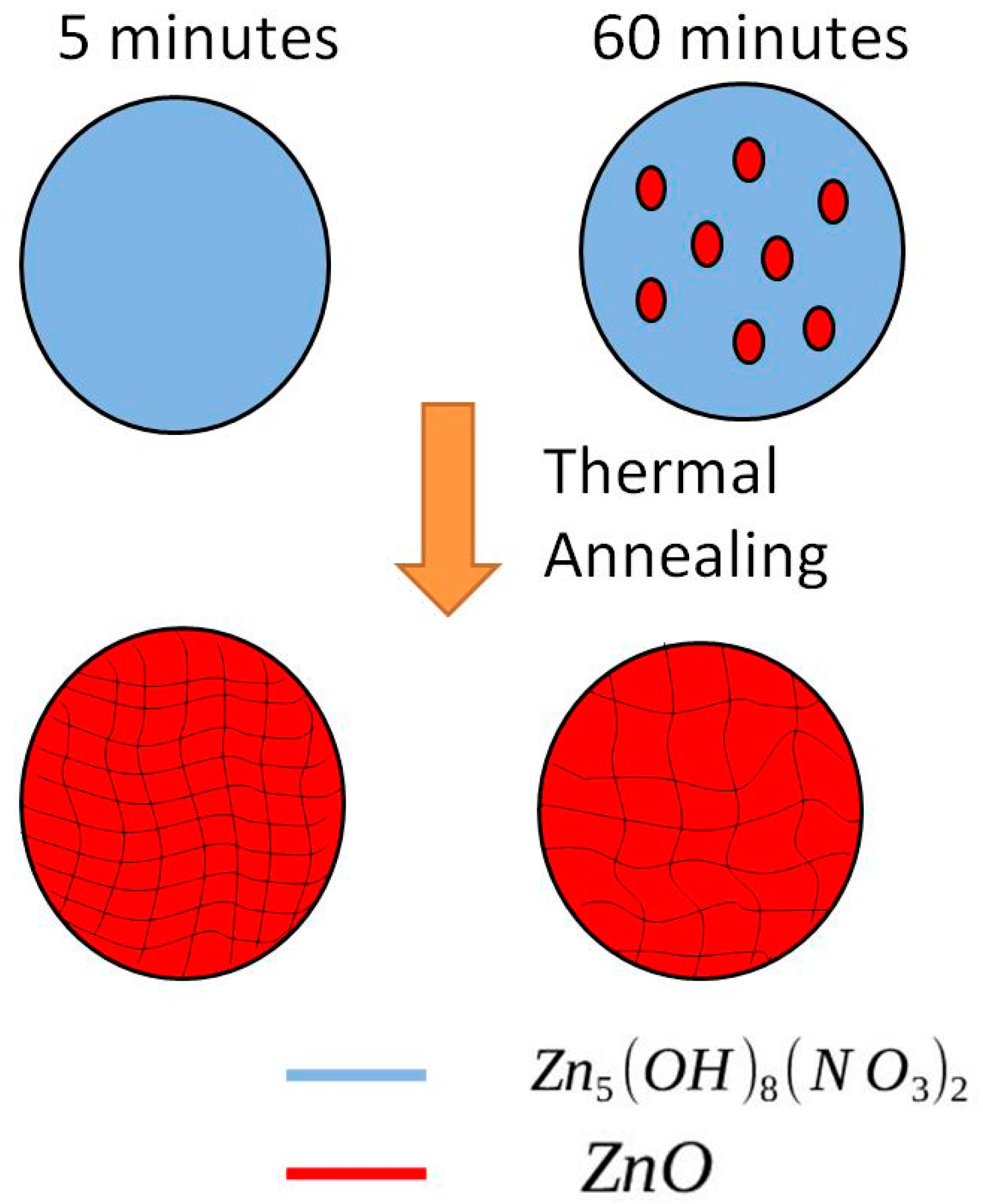
Section 2.1 depend on the growth time of the nanostructures. In particular, for a growth time of 5 min, XRD spectra revealed that the nanowalls were composed of zinc hydroxide and hydroxinitrate crystallites. For a growth time of 60 min, the nanostructures also contained ZnO crystallites. Moreover, after a thermal treatment at 300 °C in nitrogen atmosphere for 30 min, all the nanowalls were composed only by ZnO. Therefore, thermal annealing induces a transformation of the nanowalls towards pure ZnO nanowalls. Nevertheless, since the growth time has a role on the starting composition, a subsequent thermal annealing can produce different effects on the nanowalls grown for different time.
The presence of ZnO seeds in the 60 min grown samples can lead to a thermal evolution different to what occurs in the 5 min grown samples (where ZnO is not yet appeared and only zinc hydroxide and hydroxinitrate phases are present). It is known that thermal annealing up to 300 °C leads to transformation of zinc hydroxinitrate into ZnO for thermodynamic reasons [20]. Thermal annealing can induce both the nucleation and the growth of ZnO grains. In the 60-minutes growth case, where ZnO seeds already exist, the thermal annealing can directly induce the growth of ZnO grains, thus probably leading to a final structure with large ZnO crystalline domains. On the other hand, in the 5-minute grown samples the annealing has to first induce the nucleation of ZnO seeds and then their growth, probably leading to a final structure with many, but smaller, ZnO domains (Figure 9).
These final structural differences between the two samples can influence the optical and electrical properties of the ZnO nanostructures. In particular, a larger crystalline grain size can reduce the overall electrical conductance as charge transport through grain boundaries by mid-gap levels can be more effective than through a semiconducting intrinsic region. Such a hypothesis can explain the larger resistivity observed for the 60 min grown samples with respect to the 5 min ones (Figure 7). Similarly, a sample with larger grains of ZnO can induce a PL spectrum with specific features of bulk emission, since the visible photoluminescence is generated by electron-hole recombination through defect related levels placed within the gap of ZnO [18]. This can account for the shift of the PL towards lower energy for 60 min samples with respect to the 5 min ones (Figure 8).
For future realization of room temperature operating gas sensing, a higher resistivity is always preferable to enable higher sensitivity; thus, a 60 min growth seems preferable. For future realization of UV light activated gas sensors, a higher response to UV-light is desirable of course. PL signals come from radiative recombination of electron-hole pairs created by UV photon absorption. Thus, a 60-minute growth seems to be preferable with respect a 5-minute one.

5. Conclusions

In this paper, the optical and electrical properties of ZnO nanowalls synthesized by means of chemical bath deposition are investigated as a function of the growth time and annealing temperature. In particular, we assume that the initial growth time determines the successive thermal evolution of the nanostructures affecting the electrical and optical properties. We report here the results obtained for the ZnO nanowalls grown for 5 and 60 min and thermally treated at 100, 200, and 300 °C. The electric transport is favored for shorter deposition times and low annealing temperatures, while the higher resistivity is obtained for longer deposition times and higher annealing temperatures. Indeed, for longer deposition times and higher annealing temperatures, the photoluminescence spectra evidence an increased emission in the visible region with a small shoulder at 495 nm. It can be concluded that a longer deposition time, ensuring the presence of ZnO seeds just after the growth, allows to produce ZnO nanowalls with greater crystalline grains. As for gas sensing the presence of large ZnO grains is favorable for gas adsorption and electrical detection of it, a longer deposition time seems preferable for future applications in this field. Anyway, it is clear that the CBD growth time plays a key role on the synthesis of ZnO nanowalls and on their properties.

Author Contributions

Conceptualization, E.B and S.M; investigation: (1) ZnO NWLs synthesis, D.P. and E.B., (2) SEM analyses, D.P., E.B., and V.S., (3) electrical characterization, D.P. and S.M., (4) PL characterization, D.P. and G.F.; methodology: S.M., E.B., D.P.; formal analysis: D.P.; writing—original draft preparation, D.P.; writing—review and editing, E.B., G.F., S.M., V.S., project administration: E.B. and S.M.

Funding

The work has been funded by Fondi per la Ricerca di Ateneo—Piano per la Ricerca 2016/2018 (Univ. Catania, DFA). The authors also acknowledge the PON project Bio-nanotech Research and Innovation Tower (BRIT), financed by the Italian Ministry for Education, University and Research (MIUR) (Grant no. PONa3_00136).

Acknowledgments

Authors acknowledge the technical support of G. Pantè, C. Percolla and S. Tatì (CNR-IMM).

Conflicts of Interest

The authors declare no conflict of interest.

References

  1. Zhang, J.; Liu, X.; Neri, G.; Pinna, N. nanostructured Materials for Room-Temperature Gas Sensors. Adv. Mater. 2016, 28, 795–831. [Google Scholar] [CrossRef] [PubMed]
  2. Özgür, Ü.; Alivov, Y.I.; Liu, C.; Tekeb, A.; Reshchikov, M.A.; Doğanc, S.; Avrutin, V.; Cho, S.J.; Morkoç, H. A comprehensive review of ZnO materials and devices. J. Appl. Phys. 2005, 98, 041301–041404. [Google Scholar] [CrossRef]
  3. Tian, Z.R.; Voigt, J.A.; Liu, J.; Mckenzie, B.; Mcdermott, M.J.; Rodriguez, M.A.; Konishi, H.; Xu, H. Complex and oriented ZnO nanostructures. Nat. Mater. 2003, 2, 821–826. [Google Scholar] [CrossRef] [PubMed]
  4. Kumar, R.; Al-Dossary, O.; Kumar, G.; Umar, A. Zinc Oxide Nanostructures for NO2 Gas- Sensor Application; A Review. Nano-Micro Lett. 2015, 7, 97–120. [Google Scholar] [CrossRef] [PubMed]
  5. Neri, G. First fifty years of chemoresistive gas sensors. Chemosensors 2015, 3, 1–20. [Google Scholar] [CrossRef]
  6. Seiyama, T.; Kato, A. A new detector for gaseous components using semiconductor thin film. Anal. Chem. 1962, 34, 1502–1503. [Google Scholar] [CrossRef]
  7. Zhu, L.; Zeng, W. Room-temperature gas sensing of ZnO-based gas sensor: A review. Sens. Actuators A Phys. 2017, 267, 242–261. [Google Scholar] [CrossRef]
  8. Leonardi, S.G. Two-Dimensional Zinc Oxide Nanostructures for Gas Sensor Applications. Chemosensors 2017, 5, 17. [Google Scholar] [CrossRef]
  9. Xu, F.; Ho, H. Light-Activated Metal Oxide Gas Sensors: A Review. Micromachines 2017, 8, 333. [Google Scholar] [CrossRef] [PubMed]
  10. Mun, Y.; Park, S.; An, S.; Lee, C.; Kim, H.W. NO2 gas sensing properties of Au- functionalized porous ZnO nanosheets enhanced by UV irradiation. Ceram. Int. 2013, 39, 8615–8622. [Google Scholar] [CrossRef]
  11. Meng, L.; Xu, Q.; Sun, Z.; Li, G.; Bai, S.; Wang, Z.; Qin, Y. Enhancing the performance of room temperature ZnO microwire gas sensor through a combinedtechnology of surface etching and UV illumination. Mater. Lett. 2018, 212, 296–298. [Google Scholar] [CrossRef]
  12. Alenezi, M.R.; Henley, S.J.; Silva, S.R. On-chip Fabrication of High Performance Nanostructured ZnO UV Detectors. Sci. Rep. 2014, 5, 8516. [Google Scholar] [CrossRef] [PubMed]
  13. Park, S.; Kim, S.; Ko, H.; Lee, C. Light- enhanced gas sensing of ZnS- core/ ZnO-shell nanowire at room temperature. J. Electroceram. 2014, 33, 75–81. [Google Scholar] [CrossRef]
  14. Dhara, S.; Giri, P.K. Enhanced UV photosensitivity from rapid thermal annealed vertically aligned ZnO nanowire. Nanoscale Res. Lett. 2011, 6, 504–512. [Google Scholar] [CrossRef] [PubMed]
  15. Bruno, E.; Strano, V.; Mirabella, S.; Donato, N.; Leonardi, S.G.; Neri, G. Comparison of the Sensing Properties of ZnO Nanowalls-Based Sensors toward Low Concentration of CO and NO2. Chemosensors 2017, 5, 20. [Google Scholar] [CrossRef]
  16. Iwu, K.O.; Strano, V.; Di Mauro, A.; Impellizzeri, G.; Mirabella, S. Enhanced quality, growth kinetics, and photocatalysis of ZnO nanowalls prepared by chimica bath deposition. Cryst. Growth Des. 2015, 15, 4206–4212. [Google Scholar] [CrossRef]
  17. Image J. Available online: https://imagej.nih.gov/ij/docs/guide (accessed on 2 October 2012).
  18. Barbagiovanni, E.G.; Reitano, R.; Franzò, G.; Strano, V.; Terrasi, A.; Mirabella, S. Radiative mechanism and surface modification of four visible deep level defect states in ZnO nanorods. Nanoscale 2015, 8, 995–1006. [Google Scholar] [CrossRef] [PubMed]
  19. Scuderi, M.; Strano, V.; Spinella, C.; Nicotra, G.; Mirabella, S. Low-cost synthesis of pure ZnO nanowalls showing three-fold symmetry. Nanotechnology 2018, 29, 135707–135715. [Google Scholar] [CrossRef] [PubMed]
  20. Ahmadi, S.J.; Hosseinpour, M.; Javadi, F.; Tayebee, R. optimization Study on Formation and Decomposition of Zinc Hydroxynitrates to Pure Zinc Oxide Nanoparticles in Supercritical Water. Ind. Eng. Chem. Res. 2013, 52, 1448–1454. [Google Scholar] [CrossRef]
Figure 1. (a) Schematic (not to scale) representation of the interdigitated (ID) Au contacts and (b) schematization of the various steps for the synthesis of Zinc Oxide (ZnO) nanowalls (lateral-view).
Chemosensors 07 00018 g001
Figure 2. Cross section SEM images of ZnO nanowalls grown for 5 (a), 60 (b), and 120 (c) minutes.
Chemosensors 07 00018 g002
Figure 3. Plane-view SEM image of ZnO nanowalls grown for 60 min. The inset reports the intensity of the pixels in grey scale along the red line drawn across the wall (into red circle) as a function of the distance (nm).
Chemosensors 07 00018 g003
Figure 4. Average height (black squares, left black axis) and thickness (blue squares, right blue axis) of the ZnO nanowalls as a function of the growth time.
Chemosensors 07 00018 g004
Figure 5. SEM images in a tilted-view of ID contacts after the synthesis for 5 min of ZnO nanowalls.
Chemosensors 07 00018 g005
Figure 6. I-V characteristics of ZnO nowalls grown for 5 min (black lines) and for 60 min (red lines) after thermal annealing at 100 °C (a), 200 °C (b), and 300 °C (c).
Chemosensors 07 00018 g006
Figure 7. Network resistivity as a function of the annealing temperature in the sample grown for 5 (black squares) and for 60 min (red squares).
Chemosensors 07 00018 g007
Figure 8. Normalized photoluminescence spectra of ZnO nanowalls grown for 5 (solid black line) and for 60 min (dashed red line) after thermal annealing at 100 °C (a), 200 °C (b), and 300 °C (c).
Chemosensors 07 00018 g008
Figure 9. Proposed model of different phases in the samples grown for 5 and 60 min.
Chemosensors 07 00018 g009

