
Recent Advances in Silicon FET Devices for Gas and Volatile Organic Compound Sensing

Department of Physical Electronics, School of Electrical Engineering, Tel Aviv University, Tel Aviv 69978, Israel
*
Authors to whom correspondence should be addressed.
Chemosensors 2021, 9(9), 260; https://0-doi-org.brum.beds.ac.uk/10.3390/chemosensors9090260
Submission received: 25 July 2021
/
Revised: 31 August 2021
/
Accepted: 2 September 2021
/
Published: 10 September 2021
(This article belongs to the Special Issue Organic-Inorganic Hybrid Chemo- and Bio-Sensors)
Abstract
:Highly sensitive and selective gas and volatile organic compound (VOC) sensor platforms with fast response and recovery kinetics are in high demand for environmental health monitoring, industry, and medical diagnostics. Among the various categories of gas sensors studied to date, field effect transistors (FETs) have proved to be an extremely efficient platform due to their miniaturized form factor, high sensitivity, and ultra-low power consumption. Despite the advent of various kinds of new materials, silicon (Si) still enjoys the advantages of excellent and reproducible electronic properties and compatibility with complementary metal–oxide–semiconductor (CMOS) technologies for integrated multiplexing and signal processing. This review gives an overview of the recent developments in Si FETs for gas and VOC sensing. We categorised the Si FETs into Si nanowire (NW) FETs; planar Si FETs, in which the Si channel is either a part of the silicon on insulator (SOI) or the bulk Si, as in conventional FETs; and electrostatically formed nanowire (EFN) FETs. The review begins with a brief introduction, followed by a description of the Si NW FET gas and VOC sensors. A brief description of the various fabrication strategies of Si NWs and the several functionalisation methods to improve the sensing performances of Si NWs are also provided. Although Si NW FETs have excellent sensing properties, they are far from practical realisation due to the extensive fabrication procedures involved, along with other issues that are critically assessed briefly. Then, we describe planar Si FET sensors, which are much closer to real-world implementation. Their simpler device architecture combined with excellent sensing properties enable them as an efficient platform for gas sensing. The third category, the EFN FET sensors, proved to be another potential platform for gas sensing due to their intriguing properties, which are elaborated in detail. Finally, the challenges and future opportunities for gas sensing are addressed.
1. Introduction
Application of gas and chemical sensors is ubiquitous in biomedical research, preventive healthcare, food safety, automotive and chemical industries, homeland security, environmental health and pollution monitoring [1,2,3,4,5]. Thus, there is always an urgent demand for the development of a chemical/gas sensor with a low detection limit (ideally trace-level molecule detection), high sensitivity, fast response and recovery times, minimum drift, large dynamic range and excellent selectivity to the target analyte under different ambients (dry/humid). In addition to this, with the recent boom of the Internet of Things (IoT), the need for reliable and miniaturized chip-scale gas sensors with ultra-low power consumption has become increasingly important [6,7]. Among the various categories of gas sensors (resistive, nanoelectromechanical systems, etc.) [6,8,9,10] that can meet chip-scale miniaturization and low-power operation without a compromise on the sensitivity or selectivity, sensors based on field effect transistors (FETs) [1] have shown significant promising potential. A FET is a three-terminal active device in which the conduction current in the semiconductor channel is modulated by a third terminal, called the gate electrode, apart from the usual source and drain electrodes. Signal amplification is achieved by induced electric fields due to the presence of chemical analytes, which allow signals from trace molecules to be detected. To date, different types of FET configurations have been developed to gain more control of the sensing performances [1,11]. A growing interest in FET technology has enabled various materials, such as organic semiconductors [12,13,14], inorganic semiconducting nanowires and thin films [15,16,17,18], carbon nanotubes [19], graphene [20] and transition metal dichalcogenides [21] to be integrated into this platform for sensing applications. Enhanced sensing performances in terms of sensitivity, response and recovery times have been achieved by such sensors due to the large surface-to-volume ratio of these materials, enabled by nanoscale dimensions coupled with the FET architecture. However, among these, monocrystalline Si and its derivatives still enjoy the advantages of having excellent and reproducible electronic properties and compatibility with complementary metal–oxide–semiconductor (CMOS) technologies for integrated multiplexing and signal processing [22]. Advanced growth, lithographic and nanofabrication techniques can produce nanostructured Si elements for improved performance in sensing devices. Further, surface modification or chemical functionalisation of these devices allow them to achieve a desired selectivity to a specific analyte.
This review article highlights the recent advances in the development of Si FET devices for sensing gas and VOC for various applications. The article is divided into several sections. In the next section, a wide description of Si NW-based FET sensors is presented and discussed. In the third section, sensors based on planar Si FETs fabricated out of SOI or bulk Si are reviewed; this approach overcomes some of the limitations observed with Si NW-based FETs. In the fourth section, EFN FET sensors are discussed. Recent works over the past decade are highlighted in each section. In some cases, wherever relevant, details about the device architecture, functionalisation and sensing principles are discussed for the benefit of readers. The final section provides a brief overview of the challenges and opportunities for research associated with this field, and some perspectives on future developments. Most of the studies related to Si sensors are limited to sensing and monitoring chemical and biological species in aqueous solutions using Si NW sensors. To the best of our knowledge, only two reviews on Si NWs for gas sensing have been published in the recent past [5,23], but other types of Si FET gas sensors have not been reviewed in a comprehensive manner until now. We believe that this article will give a broad outlook to readers on the recent technological advancements in Si FET-based sensors for gas and VOC sensing and pave the way for future developments of gas and VOC sensors.
2. Si NW FETs for Gas Sensing
Figure 1 depicts the various kinds of Si FETs used for gas and VOC sensing. These are: (a) Si NW FETs; (b) planar Si FETs and (c) EFN FETs. Among these, Si NW FETs were demonstrated in the last two decades as highly sensitive and selective chemical sensors operating at room temperature [5,17,22,23]. Si NWs were first introduced by Leiber’s group in 2001 [17] as a promising platform for detection of various chemical and biological species. They modified the surface of Si NWs with amine and oxide functionalisation to function as a nanoscale pH sensor, which exhibited pH-dependent conductance with linearity over a large dynamic range. The protonation and deprotonation of species while sensing caused a variation in surface charge that would result in a positive or negative gating effect and cause accumulation or depletion of charge carriers, thus resulting in conductance modulation. Likewise, they also modified Si NWs with biotin or antigen for detection of streptavidin or antibody binding, respectively. Following this demonstration, Si NWs became a booming topic of interest for the past decade for various gas and chemical detection applications, with much of the focus on the synthesis methods and various functionalisation procedures to improve sensor performance metrics [5,23].
2.1. Fabrication of Si NWs
The synthesis of a highly oriented array of crystalline Si NWs over a large area is extremely desirable to minimize contact resistances and develop high-performance devices. In addition, it is also important to control the size, density and dopant concentration in order to tune the electronic properties for sensing applications. Si NWs are fabricated either by a top-down or bottom-up approach [28]. In the top-down approach, Si is shaped into a nanowire by etching the parent Si wafer, whereas in the bottom-up approach the Si NW is grown via gathering of Si atoms in a sequence. Both approaches have been adopted for the development of gas sensors [5,23]. A brief description of both fabrication methods is provided below. Interested readers are further recommended to read intensive reviews on the growth of Si nanowires in other literatures [28,29].
2.1.1. Bottom-Up Approach
The bottom-up approach is one of the oldest methods of fabrication of Si NWs. The most commonly prevalent techniques for Si NW fabrication using the bottom-up approach are thermal evaporation, molecular beam epitaxy, pulsed laser deposition and chemical vapor deposition via the vapor–liquid–solid (VLS) mechanism. Though this approach may produce high-quality NWs with small sizes, down to 10 nm [5,28,30], but control of the size, orientation and positioning of the NWs remains a persistent problem with this approach. Due to the VLS growth procedure, metal contamination due to the catalysts is a major drawback of this process that might degrade device performance. The inability to integrate with CMOS technology using this growth approach presents another limiting factor.
2.1.2. Top-Down Approach
The top-down approach for fabrication of Si NWs is CMOS-compatible and has advantages in terms of precise control of the dimensions (with a possibility of scaling down to 3 nm and below) and alignment of the NWs. This approach creates Si NW/Si nanoribbon sensors from SOI substrates or bulk wafers using advanced semiconductor process flows like lithography, deposition, etching, cleaning, passivation, etc. [5]. Si NWs can be either grown and then transferred onto an electrode substrate for sensing, or they can be directly grown on the electrodes. The latter approach allows more flexibility, as it does not require any transfer media, which might damage the Si NW surface and prove detrimental for gas sensing [31]. Recent advances in fabrication and lithography techniques have enabled the construction of a single-nanowire FET that, by virtue of its increased surface-to-volume ratio, has more adsorption sites and contributes to increased sensitivity. With advanced techniques, it has also been possible to minimise contact resistances; however, scalability and increased cost remain an issue with such devices and pose a practical challenge for real-world applications. To circumvent this problem, vertically aligned Si NW FETs have been designed for gas-sensing applications [31].
2.2. Functionalisation of Si NWs
Bare Si NWs have been used widely both in resistive and FET configurations for detection of various gases and vapours. However, to achieve selectivity, it is essential to modify the surfaces of these NWs through different approaches to create hybrid structures offering enhanced sensor performance metrics.
2.2.1. Decoration by Metal Nanoparticles (NPs)
Decorating Si NWs with metal NPs is a promising strategy for selective detection of various gas molecules. The NPs act as catalyst, thereby reducing the activation energy for adsorption of molecules and facilitating enhanced adsorption with fast reaction kinetics [32]. In this regard, NPs of palladium (Pd), platinum (Pt), gold (Au), and silver (Ag), have been utilised effectively for detection of gases such as hydrogen (H2), nitrogen dioxide (NO2) and ammonia (NH3) [32,33,34,35,36]. For example, H2 can be selectively detected by Si NW FETs by decorating it with Pd NPs [33,34]. Ahn et al. [34] fabricated a Si NW FET using the top-down approach, and decorated it with Pd NPs by electron beam evaporation for H2 detection. Their Si NW FET architecture comprised local side gates apart from a global bottom gate (Figure 2i), and the device was operated in the subthreshold regime in order to obtain maximum sensitivity. The local side gates further allowed individual addressing of the sensor in an array format. An equal biasing on the two side gates (as confirmed from simulations shown in Figure 2ii) maximized the current response due to the electrostatic interaction with the H2 molecule adsorbed on the top surface due to symmetrical channel formation at the two bottom corners of the Si NW. The side gates further modulated the electron concentration in the channel, which in turn influenced the sensitivity. Following the Pd NP decoration (1 nm thick film of discontinuous islands), the Id-Vg curve shifted to the right with an increase in the threshold voltage and a decrease in the drain current (Figure 2iii). This was attributed to the depletion of electrons in the n-type channel due to decoration with metallic Pd NPs with a high work function of 5.1 eV. They detected H2 in the range of 0.1 to 1% with a sensor response of ~3500% at 1% H2 exposure. An increase in current was observed upon H2 exposure, and the device exhibited reversible sensing behaviour for all concentrations (Figure 2iv). An increased change in current was observed in the subthreshold regime rather than in the linear regime. The H2 atoms dissociated on the surface of the Pd NPs and diffused through the Pd layer, and were absorbed onto the Pd–SiO2 interface on top of the Si NW. Then, these hydrogen atoms were polarized and gave rise to a positive dipole layer, which increased the drain current by attracting electrons flowing through the Si NW (Figure 2v).
Kim et al. [36] studied the effect of decoration of Au NPs on Si NW FETs (fabricated using the top-down technique), and evaluated the sensitivity, linearity and long-term stability of the devices upon exposure to NH3. They also found that operating the device in the subthreshold regime contributed to higher sensitivity, lower power consumption and sufficient linearity. In addition, a negligible variation was observed in the sensitivity even after 120 days, thus proving its long-term efficacy. Here also, the sensing mechanism could be explained by the work function modulation of the Au NPs on NH3 exposure, which in turn determined the carrier concentration in the channel. Sainato et al. [35] further developed a CMOS-compatible procedure to integrate the metal–Si nanostructures into chemitransistors with a high fabrication yield. Utilising metal-assisted etching with Au NPs, they integrated composite porous Si/Au nanostructures into solid-state junction FETs for detection of NO2. The sensors exhibited room-temperature operation with a fast and reliable response to NO2 in the range of 100–500 ppb, showing negligible baseline drift or variation in response time, and a sensitivity value over 48 h. This CMOS-compatible technique paved the way for efficient integration of other Si/metal nanostructures in chemitransistors on the same Si chip to develop an efficient e-nose for selective detection of gases.
2.2.2. Modification with Chemically Sensitive Inorganic and Organic Materials
Si NWs have also been modified with various chemically sensitive inorganic and organic materials for selective determination of gases and vapours. In 2015, Han et al. [37] fabricated a chemically gated FET (CGFET) in which inorganic semiconductor tin oxide (SnO2) and a Si NW (fabricated in a honeycomb structure) served as the floating gate and the conduction channel, respectively (Figure 3i,ii). The CGFET differed from conventional nanowire FETs in this case in that the sensing medium and the conduction channel were electrically decoupled, which protected the sensing layer from additional electrical stress, apart from the usual unavoidable chemical stress arising due to adsorption and desorption cycles of the target analyte. This imparted more reliability to the sensor, as the electrical stress generated at the oxide–electrode interface due to continuous current flow resulted in cracks in the oxide, metal–oxide interdiffusion and exfoliation of the electrode [37]. In addition, electromigration and Joule heating due to continuous voltage drive or current consumption proved detrimental. Another foremost reason to use this CGFET is the requirement of very low power supply or drive voltage, since the decoupling feature of the sensing and current conduction medium allows it to operate at a driving voltage of 1 V or below, making it vastly suitable for battery-operated sensors and wearable sensors. The sensing principle of this type of sensor is as follows: a pseudo potential is generated in the electrically floating sensing medium on adsorption/desorption of molecules of target analyte, and this causes a gating effect in the silicon channel underneath, thus modulating the current conduction. The device can be operated in the normally off mode, so that power is consumed only during sensing, thus drastically reducing power consumption. Moreover, operating the device in off mode (with complementary doping in the channel compared to source and drain), results in intrinsic discrimination between the oxidising and reducing gases, as depicted in Figure 3iii(a,b); this is unlike chemiresistors or the normally ON configuration of the transistor. In such devices, the current conduction occurs in both the cases, with the direction changing with the type of gas. In the CGFET (with p-type Si NW and n-channel) with SnO2 as the top film, exposure to oxidising gases such as O2 and NO causes depletion of electrons and creates a pseudo-positive gate potential, thus increasing the current conduction in the CGFET, unlike an SnO2 (n-type) based chemiresistor, in which depletion of electrons due to O2 exposure will decrease the conductance. This type of CGFET paves the way for sensing applications with low power consumption.
Haick’s group has worked extensively on Si NWs and their modification with various organic materials [26,38,39,40] in order to impart sensitivity to various VOCs, both polar and nonpolar. Paska et al. [26,41] utilised Si NWs to demonstrate selectivity towards nonpolar VOCs by modifying the Si NWs’ surface with a silane monolayer such as hydrophobic organic hexyltrichlorosilane (HTS), which otherwise has limited sensitivity towards the nonpolar VOCs. This limited sensitivity to the nonpolar VOCs can be attributed to weak adsorption of nonpolar VOCs in molecule-free sites and lack of suitable nonpolar organic functionalities, which facilitates more energy transfer from nonpolar gases (9.2 kJ/mol) compared to polar functional groups [42]. In addition, a high density of surface states at the SiO2/Si interface interferes with the molecular gating, and the high density of trap states at the air/SiO2 interface in the form of SiO− attracts water molecules and degrades the device performance [26]. The device was exposed to a number of polar (ethanol, butanol, and hexanol) and nonpolar molecules (hexane, octane, and decane), along with humidity. Figure 4i shows the schematic of the Si NW FET device that was modified with the 0% cross-linked HTS monolayer. Figure 4ii shows the conductivity change of the device for all the molecules tested. It can be seen that all polar VOCs exhibited a nonzero positive conductivity change at high negative voltages. In contrast, the water molecules showed a nonzero negative conductivity change at high negative voltages. The sensitivity of the HTS–Si NW FET sensor towards nonpolar VOCs exceeded the sensitivity towards polar molecules at approximately the same concentrations. This could be attributed to the formation of a dense HTS monolayer that successfully detected the nonpolar VOCs and prevented polar VOCs from reaching the Si NW surface. This can be explained in terms of an indirect sensor–VOC interaction, whereby the nonpolar VOC molecules induce conformational changes in the organic monolayer, affecting (i) the dielectric constant and/or effective dipole moment of the organic monolayer, and/or (ii) the density of charged surface states at the SiO2/monolayer interface, which in turn modulate the conductivity of the Si NW. In comparison, a direct electrostatic interaction between the Si NW and polar VOCs possibly changes the Si NW charge carrier concentration [26,41].
Hysteresis, which results from a lag in the response in the forward and the backward electrical characteristics of IDS vs. VBG, plays an important role in determining the stability of the electrical characteristics of these Si NW FET devices used for sensing. Paska et al. [38] further explored suitable organic modification of these devices to determine the “hysteresis phenomenon” in evaluating the quality of these Si NW FET gas sensors. The hysteresis is attributed to the surface hydroxyl sites (Si-OH). An efficient, cost-effective way to remove these trap states is to coat the Si NW surface with a monolayer of tricholorosilane (TS) molecules, which facilitates the formation of Si-O-Si bonds [41,43,44]. In this regard, it is believed that a longer chain length of the TS molecules or higher molecular density or hydrophobicity of the TS monolayers would contribute to reduced hysteresis [38,45]. However, through a series of experiments, the authors determined that the concentration of the unpassivated Si-OH groups was critical in evaluating the sensing performances of the Si NWs. The hysteresis effect, which further influenced the FET parameters, could be reduced through elimination of the free (unreacted) Si−OH groups on the Si NW surface by functionalisation with TS monolayers obtained through a two-step amine-promoted reaction (TSAPR), which is different from the direct self-assembly procedure [38]. Such chemical passivation procedures enable stable and reproducible results when using Si NW FET gas sensors in real-world humid conditions. In addition, a variety of termination groups can be obtained by further modification or reaction of the TS monolayer with desired chemical functionalities. This would in turn create a platform to discriminate the polar and nonpolar species while preserving the passivation of the surface, and subsequently the FET characteristics.
Wang et al. of Haick’s group [40] further explored the effect of the end functional group of the molecular layer with the same backbone on the sensing properties of VOCs. Threshold voltage (Vth) and hole mobility (μh) served as the sensing parameters for various VOCs. Changes in Vth (∆Vth) and μh (∆μh) showed a dependence on the VOC concentration. However, the direction of the Vth shift depended on the end group of the molecular layer. They developed a model based on dipole sensing to explain the sensing mechanism and classified the interaction between the molecular layers and VOCs into three different categories: (1) dipole−dipole interaction between the molecular layer and the polar VOCs; (2) induced dipole−dipole interaction between the molecular layers and the nonpolar VOCs; and (3) molecule tilt as a result of VOC diffusion between the chains of the molecular layer. VOC adsorption on molecular layers could occur in two ways: they could either be adsorbed on the surface of the molecule, and/or they could diffuse between the chains of the molecular layers. The dipole moment orientation of the adsorbed VOCs were determined by the electron-donating or -withdrawing nature of the end functional group, and this in turn determined the direction of the shift in Vth. On the contrary, the type and density of the functional groups played a crucial role in determining the diffusion process of the VOCs between the chain of the molecular layers, and contributed mainly to ∆μh responses. This finding could be extremely useful in designing Si NW FET sensors with molecular layers to selectively detect nonpolar VOCs that otherwise do not participate in charge transfer with the molecular layers.
Wang et al. [39] further studied the effect of chain length in the organic monolayers on the sensing performance to both polar and nonpolar VOCs. To demonstrate this, they fabricated Si NW FETs functionalised with organic layers that had a similar end group (methyl) and amide bridge bond, but differed in the alkyl chain length. Changes in the threshold voltage (ΔVth) and relative hole mobility (∆μh/μh-a) were observed to have a direct correlation with the exposed VOC concentration. ∆μh is the change in mean hole mobility due to VOC exposure, and μh-a is the mean hole mobility in air before VOC exposure. Interestingly, when exposed to a specific VOC concentration, the response in ΔVth increased with the chain length of the organic molecule, whereas Δμh/μh-a did not show any dependence on the same. An electrostatic model was developed to explain the results, which suggested that the sensor response in ΔVth was determined by the VOC concentration, VOC vapor pressure, VOC–molecular layer binding energy, and VOC adsorption-induced dipole moment changes of the molecular layer. In addition, a longer chain length of the molecular layer and relative low second-layer amide-reaction ratio enabled a large intermolecular space of the long-chain molecular layer that facilitated adsorption of more VOC molecules compared to short chain molecular layer, thus contributing to the increased ΔVth response to VOCs. The diffusion process of VOCs between the chain of molecular layers that contribute to μh responses was not so dominantly affected by the alkyl chain length, thus explaining the absence of a systematic relationship between the Δμh/μh-a and the chain length of the molecular layer.
Such modification of Si NW FETs with organic molecule receptors (different functional groups and chain lengths) further enabled an e-nose approach when combined with artificial intelligence models such as artificial neural networks [25,46,47]. In fact, Haick’s group very intelligently used multiple independent device parameters of a specific molecularly modified Si NW FET device (such as threshold voltage, hole mobility, and subthreshold swing) as input training sets for the artificial neural networks to selectively determine VOCs (in both single- and multi-component mixtures), and concentration was also determined with the least possible error [25]. This approach reduced the complex hardware, circuitry, power consumption, and tedious computational power involved with data acquisition, signal processing, and pattern-recognition analysis of signals from multiple sensors. In addition, this approach finds an excellent application in successful detection and discrimination between various diseases among patients, such as gastric cancer, lung cancer, asthma and chronic obstructive pulmonary disease, through exhaled breath [25,47].
3. Planar Si FETs for Gas Sensing
Although Si NW-based FETs have proved to be a promising platform for gas sensing, it is not feasible to implement them using large-scale conventional fabrication processes. Despite tremendous advances in the field of Si NWbased sensors, many challenges still inhibit a widespread technical and commercial use of these sensors, and limited them to academic research only. An alternative that is compatible with mass production is the use of the planar Si-based FETs fabricated out of SOI or bulk Si.
3.1. Planar Si FET Gas Sensor Based on SOI
In 2017, Fahad et al. [6] fabricated chemically sensitive FETs (CS-FETs) (using a top-down, CMOS-compatible fabrication process) based on a 3.5 nm thin Si channel on an insulator (Figure 5i). These ultrathin Si channels functioned as fully depleted transistors and formed the driving force of low-power digital electronics. Instead of an electrically active gate layer, these FETs had an electrically nonconductive, chemically sensitive layer that on interaction with the target analyte, caused a chemical gating effect and modulated the conduction current in the Si channel, and shifted the channel threshold voltage. This CSFET could act as a generic sensing platform, and by appropriate choice of chemically sensitive layers (deposited through multiple processing steps) could detect a wide range of gases. In their work, they demonstrated sensing of H2S, H2 and NO2 using Pd0.3nmAu1nm, Ni0.3nmPd1nm, and Ni1nm, respectively. Figure 5ii shows the cross sectional transmission electron microscopy (TEM) image of the Pd–Au CSFET. These CS-FETs operated as junction-less n-channel transistors in which the channel doping (degenerate doping) level was identical to the source and the drain. The charge carriers in the 3.5 nm Si channel could be fully depleted on gas exposure, thus modulating the output current by orders of magnitude. The sensing principle was based on the work function modulation of the chemically sensitive layer, causing a band realignment that shifted the threshold voltage (Figure 5iii). The interaction of the gas analyte determined the nature of the sensing response. For example, reducing gases (like H2S) (as depicted in Figure 5iv) caused a negative threshold voltage shift and current increase in n-channel devices, while a current decrease and positive threshold voltage shift took place following exposure to oxidizing gases (e.g., NO2).
The CSFETs were integrated with microheaters, which help in quick recovery of the baseline current upon withdrawal of the gas. The heaters did not play a role in the sensing mechanism of the CSFETs, thus power consumption occurred only during pulsed heating. To demonstrate the proof of concept of single-chip gas sensing, such three transistors were integrated in an array to enable multiplexed gas sensing (Figure 5v). A sequence of eight gas pulses were introduced into the chamber (Figure 5vi). Initially, three 10 ppm H2S pulses were introduced, which was successfully detected by the Pd–Au-based H2S CSFET. The H2 and NO2 sensors were unaffected due to the Ni content in their sensing layer, which inhibited any H2S interaction. For the next three pulses of 0.5% H2, the Ni–Pd CSFET showed a significant response, whereas the H2S and NO2 CSFET showed nominal responses. To further assess the selectivity between the three CSFETs, the response to a mixture of H2S and H2 gases was measured for 10 min. In the first 5 min, exposure of 10 ppm of H2S resulted in the response of only the H2S CSFET. In the next sequence, 0.5% H2 was introduced to the H2S ambient, and both the H2S and H2 CSFETs responded to their respective target gases. The NO2 CSFET in these two sequences gave a minimal response. A 100 ppm NO2 pulse was then injected for 5 min at the end that was successfully detected by the Ni-based NO2 CSFET. At the end of each sensing event, the local microheaters were turned on simultaneously to recover to the initial baseline. Thus, multiple sensors were successfully integrated in a single chip in order to detect more than three gases, enabling an efficient electronic nose. Further, the low power consumption by virtue of the 3.5 nm thin Si transistor also made it possible to integrate such a device with mobile wireless electronics.
3.2. Planar Si FET Gas Sensor Based on Bulk Si
Using a different approach, Fahad et al. [24] developed CS-FETs based on bulk Si wafers using proper device architecture and operating voltage conditions. They utilised sub-5 nm thin charge inversion layers, the conductance of which was electrostatically modulated by the work function change of the sensing layer following exposure to the analyte. The CS-FETs functioned as n-type transistors with light p-body doping (~8 × 10¹⁴ boron atoms cm−3) (Figure 6i) A sufficiently low Vt created an inversion layer of electrons at the Si/SiO2 interface, the electron density and thickness of which could be further modulated by applying a reverse bias (VSUB) to the Si substrate. Systematic TCAD simulations were performed by Fahad et al. using TCAD to understand the key parameters to control the charge inversion layer for optimal performance of the CS-FET gas sensor. To test the functional efficacy of this CS-FET platform, Ni (0.3 nm) and Pd (1 nm) were used as the sensing layer, and hydrogen-sensing characteristics of the device were tested for different concentrations ranging from 0.05% and 0.5% (diluted in dry air) at different body biases.
They observed that with increasing VSUB (from 0 to −2 V), the sensor response to 0.5% H2 increased from 291% to 1383%, as indicated in Figure 6ii,iii. Sensor linearity and sensitivity (defined as the slope of the % sensor response per ppm of H2 gas) also improved with increasing reverse bias. Moreover, the sensor platform hardly suffered from hysteresis and long-term drift. However, the applied reverse bias did not have any significant effect on the response time (Figure 6iv), as it was primarily dependent on the rate at which H2 diffused and adsorbed on the Ni–Pd sensing layer. However, larger reverse biases enabled shorter recovery times (t10) (Figure 6v). The total power consumption in all these devices did not exceed 50 µW, thus proving the efficacy of the bulk silicon CS-FETs as a low-power gas-sensing platform.
It is a challenge to detect accurate concentrations of gas in ambient with dynamically changing relative humidity and temperature, and these are the major limiting factors for air-quality monitoring and medical diagnosis. Most of the active sensing materials are responsive to slight environmental changes, which consequently change the sensor signal and make it difficult to determine the actual gas concentration in real conditions. Thus, it is of utmost importance to design gas sensors that are selective to a desired analyte for a wide range of temperatures and humidity. Various computational methods (involving signal processing utilising advanced machine-learning techniques) and experimental techniques have been found to circumvent this problem, but most of them focused on either sensor response to gas at different RH conditions or response to various humidity levels, and did not consider them as a coupled problem. The conventional metal–oxide sensors operate at a high temperature > 200 °C through use of integrated heaters that also help in removal of water molecules, but suffer from high power consumption. The CS-FETs developed by Javey’s group [48] made an attempt to overcome this problem through the use of integrated localon-chip microheaters around the sensors (Figure 7i(a,b)) and operate them at a slightly higher temperature than room temperature. In order to prove selectivity against humidity, they considered platinum NPs on trichloro (1H, 1H, 2H, 2H-perfluorooctyl) silane (FOTS) as the active sensing material for the detection of H2 gas. Figure 7i(c) depicts a top-view TEM image of Pt/FOTS on SiO2 grids. Previous studies confirmed the strong interaction between Pt and H2 gas, and increased sensor performance metrics with FOTS underneath Pt. Detection of low concentration (in ppm levels) was demonstrated, but was highly sensitive to RH change, thus making it a suitable candidate for testing this technique. Capillary condensation was expected to occur between the NPs (Figure 7i(d)), and the approximate RH level that marked the onset of this phenomenon was calculated to be 59%. They observed that with increasing microheater power (which had a linear relation with temperature), the sensor response to RH change from 50 to 90% decreased exponentially (Figure 7ii). A negligible sensor response of 11.6% was observed at a power of 372 mW corresponding to a chip temperature of 37 ± 3 °C. This was because with an increase of surface temperature, the evaporation rate of any condensed water increases; consequently the probability of water molecules adhering to the sensing material also decreases with increasing chip temperature, according to Le Chatelier’s principle [49]. A relatively low chip temperature (<100 °C) was sufficient enough to eliminate humidity, as water molecules could be evaporated instead of being boiled off. In addition, the high surface-to-volume ratio of the NPs allowed a high evaporation rate, unlike thick films in MOS sensors and other FET-based gas sensors. The sensitivity to H2 (250 ppm and 1000 ppm) hardly changed at RH levels of 50 and 90%, as depicted in Figure 7iii. The CS-FET also exhibited good selectivity against other gases like methane, carbon dioxide, ammonia, nitrogen dioxide, and sulphur dioxide, except for hydrogen sulphide, which is known for its poisoning action on catalysts like Pt [50,51,52]. Apart from the use of the microheaters to eliminate the effect of humidity on the sensor response, they also helped to maintain constant sensitivity with changing ambient temperature, as depicted in Figure 7iv,v. This further simplified the calibration process and promised low-concentration-level detection even at lower ambient temperatures for practical usage. In addition, with continuous microheater operation for 10 days at a chip temperature of 51 ± 6 °C, a negligible drift was observed, which ensured no material degradation of either the active material (Pt-FOTS) or the silane layer. The use of integrated microheaters to eliminate the response to humidity was further extended to CS-FETS with InOx thin film (~1.5 nm) as the electrically active gate material for NO2 sensing. The group further intends to improve upon the heating power needed to reach the chip temperature levels in order to eliminate humidity levels by working on various aspects of the microheater material selection and design. Further systematic studies with a library of sensing materials are required to see their long-term sustainability to the emitted heat from the microheaters. Nonetheless, the study provided a platform to reduce the practical challenges associated with sensing in ambient conditions with different humidity and temperature levels.
Yuan et al. of the same group demonstrated multiplexed gas detection at room temperature associated with food spoilage through the use of an integrated CS-FET array [53]. NH3 and H2S acted as marker gases for spoilt high-protein foods like eggs, diary, and meat and hence served as indicators for freshness of these foods. Sensors should be able to detect these gases at very low concentrations (less than 100 ppb) to suggest the possible onset of spoilage at an early stage. In addition, humidity plays an important role in affecting food storage and spoilage, and hence should be simultaneously monitored along with NH3 and H2S. N-doped bulk CS-FETs were developed with electrically floating thin films of ruthenium (Ru), Ag, and SiOx to selectively detect NH3, H2S and humidity respectively, through a chemical gating effect. These materials were chosen for the following reasons: Ru is known to show catalytic effects towards NH3 [53,54,55]; Ag is known to bind strongly to sulphur-containing compounds [56]; and the abundant oxygen vacancies formed due to rapid deposition of SiOx react strongly with humidity [57]. Figure 8i depicts the device structure of such CS-FETs. For practical food-spoilage monitoring, egg and pork belly were chosen as representative samples. Prior to that, each sensor in the array was tested at various concentrations of NH3, H2S, and humidity to determine sensitivity and selectivity, as depicted in Figure 8ii. The limit of detection achieved was 10 ppb for both gases, which was well below the desired limit, as stated previously. They attributed the origin of the sensor signal to work-function variation of the electrically floating gate materials. The sensitivity obtained with NH3 and H2S FETs was superior to recently published results. The authors also checked for stability, hysteresis and long-term performance of these sensors. All the sensors exhibited good stability both at low and high concentrations, with slight drift in the baseline signal between cycles. Low hysteresis was also observed, and sensor performance was also retained after a month. The inorganic sensing layers allowed more robustness and retention of sensor performances beyond a long period of time. The multi-CS-FET array was also tested for selectivity towards other interfering common air pollutant gases such as CO, SO2, HCHO and NO2, and the sensors exhibited negligible responses to these gases, thus proving its strong potential application in food spoilage and waste monitoring. The CSFET array was then integrated with a custom printed circuit board and circuitry to perform controlled measurements of food spoilage. With suitable choice of functional materials, the platform can further serve as a portable system to detect various gaseous markers of lung or gastrointestinal diseases at ppb levels present in exhaled breath, or to monitor toxic gas leaks in industrial plants.
4. EFN FET Devices for Gas Sensing
4.1. Introduction to the EFN FET Sensor
Another class of Si-channel-based FET gas sensors are the SOI-based EFN gas sensors, which utilise multigate sensing technology. As the name suggests, the NW-like conducting channel in these sensors is not created physically, but by electrostatic control of the conduction channel through appropriate biasing of various junction and back gates, as will be explained below. The EFN gas sensor was first introduced as a specific, real-time, label-free biosensor for detection of protein–protein interactions at femtomolar concentrations [58]. The schematic of an n-type accumulation-type EFN device is shown in Figure 9i. As depicted, the n-doped conducting channel forms two back-to-back junctions with two p+-doped regions on its sides that serve as junction gates. The p-type substrate below the buried oxide layer (BOX) forms the back gate. The EFN gas sensor resembles the G4 field-effect transistor developed in 2002 [59,60,61], with the exception that the top metal gate is replaced by the top molecular gate provided by the target analyte molecules [27]. A negative bias on the back gate (VBG) depletes the SOI of majority carriers (electrons), and the accumulated channel is confined to the top of the SOI (Figure 9ii). Thus, the “height” of the channel is determined by the back gate potential in the bulk SOI. A negative bias on the junction gates (VJG) operates the p+-n junctions in reverse mode, thus increasing the depletion regions on both sides of the metallurgical junctions. A higher reverse bias on both sides will eventually create larger depletion regions and confine the conducting channel to narrower dimensions (also see Figure 9ii). Thus, the width of the channel in the bulk SOI is predominantly controlled by the applied junction gate voltages. Figure 9iii depicts an elongated channel with VBG = 0 V and negative VJGs. Thus, appropriate biasing of the various gate voltages allow tuning of the width and height, and hence the shape of the conducting channel. An application of an asymmetric bias to the VJGs (VJG1 not equal to VJG2) controls the lateral position of the conducting channel (see Figure 9iv, where VJG1 is not equal to VJG2, and VBG is negative). An equal bias on the two junction gates (VJG1 = VJG2) will position the EFN in the middle. A gradient of dopant concentration will also allow the EFN channel to be located in the middle and the bottom of the bulk SOI, such that concentrations are maximised in the middle and bottom of the SOI, respectively (see Figure 9v,vi, respectively). However, it should be noted that reverse biasing of the p-n junctions is limited by the junction breakdown voltage determined by the dopant concentration (donors) of the bulk SOI. A smaller dopant concentration will enable a higher reverse bias, but can result in the absence of carriers for the formation of the channel.
Thus, a SOI-based EFN is inherently different from the conventional top-down or bottom-up synthesized Si NWs. In the case of Si NWs, a single recipe of fabrication will create a NW of desired dimensions and electrical properties, thus limiting its flexibility and sensing properties. However, in the case of the EFN, the nanowire dimensions and location can be suitably tuned electrostatically post-fabrication by application of various gates voltages. This in turn also controls the channel-conducting properties and the sensing performance metrics of the EFN, which can be tailored with regard to specific target analytes. In addition, since the EFN is based on SOI technology, it provides high bulk mobility, high signal-to-noise ratio, crystallinity, and homogeneous dopant distribution [27]. Moreover, the EFN sensors are fabricated by standard state-of-the-art CMOS-compatible fabrication techniques, which enables EFN to be a scalable, low-cost, robust platform for gas sensing [27]. Another advantage of the EFN over conventional Si NWs fabricated by the bottom-up synthesis method is that it does not suffer from inhomogeneous dopant distribution and the presence of metal catalysts. Moreover, in e case of Si NWs, suitable functionalisation is required to achieve selectivity based on the electronic nose principle. As will be shown in more detail below, it was demonstrated that when using a single unmodified EFN device, selectivity was achieved for various VOCs through a combination of applied junction and back gates [63]. However, surface modification can be very efficient in the case of the EFN, as we have recently shown for detection of hydrogen [64]. The modified surface can attract more gas molecules, resulting in greater charge transfer/dipole layers, etc., causing stronger modulation of the conducting channel. In the case of a surface-modified Si NW, the NW itself forms both the sensing and conducting channel between the source and drain, and its constant exposure to current might generate electrical stress apart from the usual chemical stress, and thus degrade the electronic properties. However, since in an EFN, the channel is electrostatically coupled to the surface, which acts as a molecular gate, chances of degradation in electronic properties of the channel due to multiple uses is not a problem, which provides a greater lifetime and stability for the devices [27].
4.2. EFN Sensor for Sensing Polar and Nonpolar VOCs
Most of the gas and VOC sensors based on Si NWs and other nanostructured materials [65,66] reported have achieved a high sensor response, low limit of detection and fast sensor kinetics. However, it is also important to address the dynamic range (total spectrum of concentration) for a target gas or an analyte, particularly at room temperature. The dynamic range of a sensor in the case of nanostructured-material-based gas sensors is limited by the number of adsorption sites, and the upper threshold is controlled by saturation in response to high concentrations, beyond which the sensor is not able to discriminate properly each concentration. It is also desirable that increased dynamic range will be achieved, along with a high sensor response and low limit of detection. In the case of the EFN, all these parameters could be successfully achieved by appropriate tuning of the size and shape of the nanowire conducting channel in the SOI [67]. A broad dynamic range was reported for ethanol (~26–2030 ppm) and acetone (~40–2800 ppm), with a reasonably high sensor response (>20%) throughout the whole range [67]. This is depicted in Figure 10i–vi, in which the device response for a wide range of EFN diameters and shapes corresponding to different VJG and VBG following exposure to varying concentrations of ethanol and acetone are shown. Figure 10i,ii depict the sensor response to ethanol and acetone, respectively, at various VJG and a constant VBG of −3 V. The corresponding effective diameter of the EFN for the different VJG at VBG = −3 V ranged from 29 nm (VJG = −0.8 V) up to 52 nm (VJG = −0.2 V). Due to the increased EFN diameter at more positive VJG, a wider channel existed, due to which the response decreased. At a given concentration, ethanol showed more sensitivity than acetone, which the authors attributed to the hydroxyl group of ethanol, which is more likely to undergo stronger interactions with the Si-OH surface sites than acetone, and the additional weak bond of ethanol interacting with the Si-O-Si sites [68,69]. Figure 10iii,iv illustrate the response to ethanol and acetone, respectively, at various VBGs and a constant VJG of −0.7 V. Figure 10v,vi clearly demonstrate the different optimum gate biases to be applied to the EFN device to span the proposed dynamic range.
As can be observed in Figure 10, a smaller EFN corresponding to more negative VJG and VBG was highly sensitive to lower concentrations, and saturation in response occurred early, thus contributing to a lower dynamic range. On the contrary, a wider EFN corresponding to a less negative VJG and VBG had a higher detection limit (estimated from the signal-to-noise ratio); the sensor response varied linearly even in the higher concentration regime, and had a higher upper threshold of concentration detection. It should be noted that surface potential changed rapidly with a small change in VJG; however, the influence of the VBG change was not very much. Thus, the shape and size of the EFN nanowire was controlled electrostatically, which resulted in tunable sensor response and large dynamic range using a single device [67].
While detecting polar VOCs is comparatively simpler due to their intrinsic dipole moments, it is more challenging to sense nonpolar VOCs. Nonpolar VOCs were detected by Si NWs through modification of the dielectric constant and/or effective dipole moment of the organic layer functionalised on the Si NW surface by inducing conformational changes in the monolayer [26,39,40,41]. A change in the density of charged surface states at the SiO2/monolayer interface is also possible. However, if nonpolar molecules could be detected through an unmodified Si device, it would eliminate the need for a tedious search for a specific coating to selectively detect a target nonpolar analyte. The EFN sensor proved to be a promising platform for addressing this challenge as well. Nandhini et al. [70] demonstrated successful detection of nonpolar n-alkanes along with polar n-alcohols through an unmodified EFN. They also found the effect of increasing alkyl chain length on the sensing properties of EFN for both the groups of molecules, with a longer alkyl chain length contributing to a greater response. Figure 11i demonstrates the dynamic sensor response of the EFN to various alcohols (ethanol, butanol, and hexanol) and alkanes (hexane, octane, and decane). The sensor exhibited significant responses only for higher concentrations of alkanes compared to polar alcohols due to their nonpolar nature. As evident from the figure, a longer alkyl chain length contributed to a higher response. Figure 11ii demonstrates the shift in the threshold voltages (both back and junction gates) with respect to different concentrations of alcohols and alkanes. A higher positive shift was observed in the case of higher alkyl chain lengths. Moreover, a positive shift indicated a negative gating effect due to induced negative charges on the EFN surface depleting the EFN channel and reducing the current, consistent with the observed dynamic sensor responses.
Several potential influencing factors were determined by the authors that might contribute to the sensing mechanism, such as interaction of molecules with the EFN SiO2 surface, intermolecular interaction strength (and other molecular properties) and the surface-induced electric field on the EFN surface [70]. The dipole moments of the various tested alcohols varied (1.55–1.69 D) compared to the nonpolar alkanes, which contributed to the relatively weak sensor responses of the alkanes at equivalent concentrations. However, the dipole moments of the tested alcohols being largely similar could not solely explain the increased response due to the increasing chain length. The authors attributed this to the increased probability for intermolecular interactions arising due to more potential interaction sites due to more CHx groups on longer alkyl chain lengths. This contributed to a more compact, ordered and stabilised adsorption layer on the EFN surface, resulting in enhanced surface coverage [71]. Similar to alkanes, with increasing alkane chain length, adsorption energy increases, and an increased tendency to layer formation occurs, contributing to a more ordered and strongly interacting multilayer alkane structure on the EFN surface with better surface coverage. It also is shown in Figure 11iii that a fringing electric field was induced by the p+-n regions on the EFN surface, which might also have played a crucial role in the sensing. As the reverse bias on the junction gates was increased on either side of the channel, it increased the induced electric field in the space charge region. This induced electric field was of the order of 106 V/cm for the applied junction gate bias in the range of 0–2 V. As observed in Figure 11iv, as the negative bias on the junction gate was increased, the sensor response also increased. A narrow channel corresponding to a more negative junction gate also was a contributing factor to the increased sensor response, as a small channel was more sensitive to minute changes in surface potential induced by the adsorption of analytes. In addition, this surface electric field might contribute to induced dipole moments in the polarizable alkane molecules, which can contribute to their sensor response at higher concentrations. In addition, polarizability of molecules is known to increase with molecule size, and decreased vapour pressure due to an increase in chain length. This might be another contributing factor to increased sensor response with higher alkanes. Thus, the authors offered a very good discussion of several contributing factors for the sensing mechanism [70].
Henning et al. further explored the effect of the surface fringing field of the EFN to control surface–analyte interaction in order to display selective detection of ethanol and n-butylamine at room temperature using a single unmodified EFN [72]. Usually, organic linker molecules are used to functionalise the SiO2 dielectric surface in order to render selectivity to different VOCs [39,40,41]. However, this complicates the device fabrication process and hampers the long-term stability of the devices, especially after prolonged and repetitive exposure to the analyte and ambient air [72]. As such, fringing-field-controlled chemical sensing promises an innovative approach to demonstrate selectivity without the need for external surface modifications.
The authors simulated the fringing field strength to be in the range of 0.5 × 10⁵ to 2.5 × 10⁵ V/cm when the junction gate bias was varied from 0.5 to −2.5 V. Beyond 0.5 V, significant p-n junction diffusion leakage currents arose, which marked the upper threshold limit. Below −2 V, the n-Si channel was fully depleted of electrons and marked the lower threshold limit. As seen in Figure 12i,ii, the electric field in the case of negative junction gate penetrated into the ambient at the top of the dielectric and could influence the adsorption of VOC analytes. It should be mentioned that a change in doping profile of the n channel would allow a different range of junction gate biases. The fringing field was strongest above the p-n junction and then decreased exponentially in the ambient. Figure 12iii depicts the shift in back gate threshold voltages due to ethanol exposure at specific positive and negative junction gates. Figure 12iv shows the sensor response of the EFN to 2000 ppm of ethanol at various junction gates. The sensor response correlated with the simulated fringing field strength (red). Figure 12v depicts the EFN sensor responses to equal concentrations of ethanol (top) and n-butylamine (below). Figure 12vi depicts how the surface electric field could selectively detect ethanol and butylamine. A suitable choice of the working point (VJG = 0.2 V and VD = 0.4 V) facilitated discrimination between the molecules (Figure 12vi, solid lines). Thus, efficient tuning of the intrinsic sensor response is shown, with the variation of the fringing field strength controlled by the applied junction gate biases.
4.3. A Single Unmodified EFN Sensor as a Platform for Obtaining Electrostatic Selectivity towards VOCs
Niharendu et al. [63] further extended this concept of electrostatic selectivity towards highly selective detection (~90%) of homologous and different functional groups containing VOCs. The homologous alcohols such as hexanol, butanol, propanol and ethanol were tested to study the effect of the chain length of VOCs on the sensing selectivity. Ketone (acetone) and carboxylic acid (acetic acid) were selected, as they possess the same chain lengths as propanol and ethanol, respectively, and facilitated evaluating the effect of functional (head) groups of VOCs in the sensing process. Conventional e-noses require an array of sensors coated with analyte specific organic or inorganic layers to achieve selectivity. However, the authors here very intelligently used multiple sensing parameters of the EFN (threshold voltage, Vth and the drain-source on current, Ion for both junction and back gates) as input for the training of the machine-learning-based classifier in order to achieve selective detection of the targeted VOCs. Different concentrations of the various analytes were chosen such that identical sensor responses (~0.95) were obtained in order to obtain concentration-independent selectivity. The back gate parameters, Vth (BG) and Ion (BG), of the EFN sensor were extracted from IDS vs. VBG measurements at different VJG and VDS. Similarly, the junction gate parameters, Vth (JG) and Ion (JG), of the EFN sensor were extracted from the IDS vs. VJG measurements at different VBG and VDS. Measurements were carried out before and after exposure to the analyte, and ∆Vth and ∆Ion were calculated for all VOCs. Each VOC produced a different pattern of ∆Vth and ∆Ion as a function of the drain-source and back and junction gate potentials. This served as a ‘fingerprint’ corresponding to each VOC, which ultimately enabled the sensor to achieve selectivity between them. Figure 13 demonstrates the ∆Vth (BG) at various VJG for the different groups of molecules (top row), and linear discriminant analysis (LDA) as a tool to visualise the separability between the measured changes in sensor parameters for different VOCs (bottom row). Different machine-learning-based classifiers, like support vector machines, Adaboost, decision tree and random forest were further utilised to selectively detect targeted VOCs. The average accuracy in each case was close to 90%. LDA poorly discriminated between the homologous alcohols, but various machine-learning classifiers were used to successfully discriminate them. Thus, a single unmodified EFN was capable of successfully differentiating the targeted VOCs using appropriate biasing of the various gate voltages.
5. Conclusions and Future Perspectives
High-performance gas sensors are always in demand for employment in environmental health monitoring, industries and medical diagnostics. As such, gas sensors based on FET technology provide a potential platform due to their high sensitivity, possibility of chip-scale miniaturization and ultralow power consumption. Among the plethora of gas-sensing materials available to date, Si still enjoys the benefits of excellent and reproducible electronic properties. Moreover, being a CMOS-compatible material, it allows scalability of the sensors. The current review presented the recent developments in Si FETs for gas and VOC sensing. Specifically, advancements in three different categories of Si FET-based sensors have been covered, namely Si NW-based FET sensors, planar Si FET sensors and EFN FET sensors. Sensors from each category have both advantages and disadvantages, which have been described. An attempt also was made to delve into the different organic and inorganic functionalisations in each category of sensors to obtain selectivity. Further, sensing mechanisms, which are necessary to understand each category of sensors, were also discussed. The Si NW FET sensors show excellent sensing capability due to their large surface-to-volume ratio, but large-scale commercialisation of these sensors is still far from realization due to extensive lithographic techniques and complicated fabrication procedures, troubles with alignment procedures, and homogeneous doping issues. The planar Si FETs made from SOI or bulk Si enjoy much simpler fabrication procedures and also provide high sensitivity towards numerous gases; this make them more feasible for real-world applications. Lastly, the EFN gas sensors that resemble the G4 transistors, with their top metal gate replaced by molecular gating induced by analytes, were first presented in 2013. Over the past decade, through numerous developments, this type of sensor has proved to be a promising platform for gas sensing. The most intriguing feature of the EFN FET sensors is the post-fabrication formation of a virtual nanowire electrostatically, which forms the conducting channel by application of suitable gate biases. We discussed how a small change in surface potential due to analyte adsorption would drastically modulate the current in the conducting channel, which eventually leads to a huge shift in threshold voltages. Further, the shape and size of the nanowire could be suitably tuned by appropriate biasing of the various gates. This leads to several degrees of freedom or parameters whose measured changes due to analyte exposure can serve as inputs to machine-learning classifiers and pattern-recognition algorithms for selective determination of gases. A selectivity against various VOCs has been achieved with a single unmodified device. This terminated the tedious need to search for a suitable functionalisation material for selective gas sensing. Nonetheless, proper surface modification would contribute to enhanced sensing performances. In a future direction, an array of EFN sensors on a single chip could be developed to mimic the e-nose with much improved sensitivity and selectivity without complex functionalisation procedures, but with different devices with different gate biases. With improved microelectronics, the goal of the development of electronic circuits compatible with the different biasing concepts (individual addressing of the devices through various gate biases) can be met in the near future. Currently, desorption of gases with this technology is achieved through ex-situ heating, so an advanced design with in situ heater membranes would provide a better choice. Since it is already being produced at a large scale at a commercial fabrication facility, we tend to believe that the EFN technology will have a significant impact on the gas-sensing industry in the coming years, though more rigorous experiments at an academic scale are required. In addition, EFN has proved to be an efficient temperature-sensing platform. Thus, an integrated platform with gas, temperature and humidity sensors would be versatile and suitable for implementation in the IoT era.
We hope that this work will lead to improved FET-based sensors and ultimately lead to reliable and selective commercial gas-sensing devices for the benefit of humanity.
Funding
A.M. and Y.R. would like to acknowledge the grant from the Office of Naval Research, USA (ONR grant number N000141912010).
Conflicts of Interest
The authors declare no conflict of interest.
References
- Hong, S.; Wu, M.; Hong, Y.; Jeong, Y.; Jung, G.; Shin, W.; Park, J.; Kim, D.; Jang, D.; Lee, J.H. FET-type gas sensors: A review. Sens. Actuators B Chem. 2021, 330, 129240. [Google Scholar] [CrossRef]
- Dai, J.; Ogbeide, O.; Macadam, N.; Sun, Q.; Yu, W.; Li, Y.; Su, B.L.; Hasan, T.; Huang, X.; Huang, W. Printed gas sensors. Chem. Soc. Rev. 2020, 49, 1756–1789. [Google Scholar] [CrossRef] [PubMed]
- Majhi, S.M.; Mirzaei, A.; Kim, H.W.; Kim, S.S.; Kim, T.W. Recent advances in energy-saving chemiresistive gas sensors: A review. Nano Energy 2021, 79, 105369. [Google Scholar] [CrossRef] [PubMed]
- Bag, A.; Lee, N.E. Gas sensing with heterostructures based on two-dimensional nanostructured materials: A review. J. Mater. Chem. C 2019, 7, 13367–13383. [Google Scholar] [CrossRef]
- Akbari-Saatlu, M.; Procek, M.; Mattsson, C.; Thungström, G.; Nilsson, H.E.; Xiong, W.; Xu, B.; Li, Y.; Radamson, H.H. Silicon nanowires for gas sensing: A review. Nanomaterials 2020, 10, 2215. [Google Scholar] [CrossRef] [PubMed]
- Fahad, H.M.; Shiraki, H.; Amani, M.; Zhang, C.; Hebbar, V.S.; Gao, W.; Ota, H.; Hettick, M.; Kiriya, D.; Chen, Y.Z.; et al. Room temperature multiplexed gas sensing using chemical-sensitive 3.5-nm-thin silicon transistors. Sci. Adv. 2017, 3, e1602557. [Google Scholar] [CrossRef] [PubMed] [Green Version]
- Banerjee, A.; Khan, S.U.H.; Broadbent, S.; Bulbul, A.; Kim, K.H.; Noh, S.; Looper, R.; Mastrangelo, C.H.; Kim, H. Molecular bridge-mediated ultralow-power gas sensing. Microsyst. Nanoeng. 2021, 7, 1–11. [Google Scholar] [CrossRef]
- Li, M.; Tang, H.X.; Roukes, M.L. Ultra-sensitive NEMS-based cantilevers for sensing, scanned probe and very high-frequency applications. Nat. Nanotechnol. 2007, 2, 114–120. [Google Scholar] [CrossRef] [PubMed]
- Hung, C.M.; Le, D.T.T.; Van Hieu, N. On-chip growth of semiconductor metal oxide nanowires for gas sensors: A review. J. Sci. Adv. Mater. Devices 2017, 2, 263–285. [Google Scholar] [CrossRef]
- Suh, J.H.; Cho, I.; Kang, K.; Kweon, S.J.; Lee, M.; Yoo, H.J.; Park, I. Fully integrated and portable semiconductor-type multi-gas sensing module for IoT applications. Sens. Actuators B Chem. 2018, 265, 660–667. [Google Scholar] [CrossRef]
- Sheibani, S.; Capua, L.; Kamaei, S.; Akbari, S.S.A.; Zhang, J.; Guerin, H.; Ionescu, A.M. Extended gate field-effect-transistor for sensing cortisol stress hormone. Commun. Mater. 2021, 2, 1–10. [Google Scholar] [CrossRef]
- Pfattner, R.; Foudeh, A.M.; Chen, S.; Niu, W.; Matthews, J.R.; He, M.; Bao, Z. Dual-gate organic field-effect transistor for pH sensors with tunable sensitivity. Adv. Electron. Mater. 2019, 5, 1–9. [Google Scholar] [CrossRef] [Green Version]
- Borges-González, J.; Kousseff, C.J.; Nielsen, C.B. Organic semiconductors for biological sensing. J. Mater. Chem. C 2019, 7, 1111–1130. [Google Scholar] [CrossRef]
- Wu, M.; Hou, S.; Yu, X.; Yu, J. Recent progress in chemical gas sensors based on organic thin film transistors. J. Mater. Chem. C 2020, 8, 13482–13500. [Google Scholar] [CrossRef]
- Knopfmacher, O.; Tarasov, A.; Fu, W.; Wipf, M.; Niesen, B.; Calame, M.; Schönenberger, C. Nernst limit in dual-gated Si-nanowire FET sensors. Nano Lett. 2010, 10, 2268–2274. [Google Scholar] [CrossRef]
- Tseng, C.W.; Wen, C.; Huang, D.C.; Lai, C.H.; Chen, S.; Hu, Q.; Chen, X.; Xu, X.; Zhang, S.L.; Tao, Y.T.; et al. Synergy of ionic and dipolar effects by molecular design for pH sensing beyond the Nernstian limit. Adv. Sci. 2020, 7, 290. [Google Scholar] [CrossRef]
- Cui, Y.; Wei, Q.; Park, H.; Lieber, C.M. Nanowire nanosensors for highly sensitive and selective detection of biological and chemical species. Science 2001, 293, 1289–1292. [Google Scholar] [CrossRef]
- Feng, P.; Shao, F.; Shi, Y.; Wan, Q. Gas sensors based on semiconducting nanowire field-effect transistors. Sensors 2014, 14, 17406–17429. [Google Scholar] [CrossRef] [Green Version]
- Bondavalli, P.; Legagneux, P.; Pribat, D. Carbon nanotubes based transistors as gas sensors: State of the art and critical review. Sens. Actuators B Chem. 2009, 140, 304–318. [Google Scholar] [CrossRef]
- Zhan, B.; Li, C.; Yang, J.; Jenkins, G.; Huang, W.; Dong, X. Graphene field-effect transistor and its application for electronic sensing. Small 2014, 10, 4042–4065. [Google Scholar] [CrossRef]
- Cao, J.; Chen, Q.; Wang, X.; Zhang, Q.; Yu, H.-D.; Huang, X.; Huang, W. Recent development of gas sensing platforms based on 2D atomic crystals. Research 2021, 2021, 9863038. [Google Scholar] [CrossRef]
- Li, J.; Rogers, J.A. Interface engineering of Si hybrid nanostructures for chemical and biological sensing. Adv. Mater. Technol. 2020, 5, 2000380. [Google Scholar] [CrossRef]
- Cao, A.; Sudhölter, E.J.R.; de Smet, L.C.P.M. Silicon nanowire-based devices for gas-phase sensing. Sensors 2013, 14, 245–271. [Google Scholar] [CrossRef]
- Fahad, H.M.; Gupta, N.; Han, R.; Desai, S.B.; Javey, A. Highly sensitive bulk silicon chemical sensors with sub-5 nm thin charge inversion layers. ACS Nano 2018, 12, 2948–2954. [Google Scholar] [CrossRef]
- Shehada, N.; Brönstrup, G.; Funka, K.; Christiansen, S.; Leja, M.; Haick, H. Ultrasensitive silicon nanowire for real-world gas sensing: Noninvasive diagnosis of cancer from breath volatolome. Nano Lett. 2015, 15, 1288–1295. [Google Scholar] [CrossRef] [PubMed]
- Paska, Y.; Stelzner, T.; Christiansen, S.; Haick, H. Enhanced sensing of nonpolar volatile organic compounds by silicon nanowire field effect transistors. ACS Nano 2011, 5, 5620–5626. [Google Scholar] [CrossRef] [PubMed]
- Shalev, G. The electrostatically formed nanowire: A novel platform for gas-sensing applications. Sensors 2017, 17, 417. [Google Scholar] [CrossRef] [Green Version]
- Hobbs, R.G.; Petkov, N.; Holmes, J.D. Semiconductor nanowire fabrication by bottom-up and top-down paradigms. Chem. Mater. 2012, 24, 1975–1991. [Google Scholar] [CrossRef] [Green Version]
- Schmidt, V.; Wittemann, J.V.; Senz, S.; Gósele, U. Silicon nanowires: A review on aspects of their growth and their electrical properties. Adv. Mater. 2009, 21, 2681–2702. [Google Scholar] [CrossRef]
- Jia, C.; Lin, Z.; Huang, Y.; Duan, X. Nanowire electronics: From nanoscale to macroscale. Chem. Rev. 2019, 119, 9074–9135. [Google Scholar] [CrossRef] [PubMed]
- Mirzaei, A.; Kang, S.Y.; Choi, S.W.; Kwon, Y.J.; Choi, M.S.; Bang, J.H.; Kim, S.S.; Kim, H.W. Fabrication and gas sensing properties of vertically aligned Si nanowires. Appl. Surf. Sci. 2018, 427, 215–226. [Google Scholar] [CrossRef]
- Kolmakov, A.; Chen, X.; Moskovits, M. Functionalizing nanowires with catalytic nanoparticles for gas sensing application. J. Nanosci. Nanotechnol. 2008, 8, 111–121. [Google Scholar] [CrossRef]
- Choi, B.; Ahn, J.H.; Lee, J.; Yoon, J.; Lee, J.; Jeon, M.; Kim, D.M.; Kim, D.H.; Park, I.; Choi, S.J. A bottom-gate silicon nanowire field-effect transistor with functionalized palladium nanoparticles for hydrogen gas sensors. Solid State Electron. 2015, 114, 76–79. [Google Scholar] [CrossRef]
- Ahn, J.H.; Yun, J.; Choi, Y.K.; Park, I. Palladium nanoparticle decorated silicon nanowire field-effect transistor with side-gates for hydrogen gas detection. Appl. Phys. Lett. 2014, 104, 083701. [Google Scholar] [CrossRef]
- Sainato, M.; Strambini, L.M.; Rella, S.; Mazzotta, E.; Barillaro, G. Sub-parts per million NO2 chemi-transistor sensors based on composite porous silicon/gold nanostructures prepared by metal-assisted etching. ACS Appl. Mater. Interfaces 2015, 7, 7136–7145. [Google Scholar] [CrossRef] [PubMed]
- Fet, A.S.N.; Kim, D.; Park, C.; Choi, W.; Shin, S.; Jin, B.; Baek, R.; Lee, J.; Member, S. Improved long-term responses of sensor for NH3 detection. IEEE Sens. J. 2020, 20, 2270–2277. [Google Scholar]
- Han, J.W.; Rim, T.; Baek, C.K.; Meyyappan, M. Chemical gated field effect transistor by hybrid integration of one-dimensional silicon nanowire and two-dimensional tin oxide thin film for low power gas sensor. ACS Appl. Mater. Interfaces 2015, 7, 21263–21269. [Google Scholar] [CrossRef]
- Paska, Y.; Haick, H. Interactive effect of hysteresis and surface chemistry on gated silicon nanowire gas sensors. ACS Appl. Mater. Interfaces 2012, 4, 2604–2617. [Google Scholar] [CrossRef]
- Wang, B.; Haick, H. Effect of chain length on the sensing of volatile organic compounds by means of silicon nanowires. ACS Appl. Mater. Interfaces 2013, 5, 5748–5756. [Google Scholar] [CrossRef] [PubMed]
- Wang, B.; Haick, H. Effect of functional groups on the sensing properties of silicon nanowires toward volatile compounds. ACS Appl. Mater. Interfaces 2013, 5, 2289–2299. [Google Scholar] [CrossRef]
- Paska, Y.; Stelzner, T.; Assad, O.; Tisch, U.; Christiansen, S.; Haick, H. Molecular gating of silicon nanowire field-effect transistors with nonpolar analytes. ACS Nano 2012, 6, 335–345. [Google Scholar] [CrossRef] [PubMed]
- Bennett, M.E.; Alexander, W.A.; Lu, J.W.; Troya, D.; Morris, J.R. Collisions of polar and nonpolar gases with hydrogen bonding and hydrocarbon self-assembled monolayers. J. Phys. Chem. C 2008, 112, 17272–17280. [Google Scholar] [CrossRef]
- Mcalpine, M.C.; Ahmad, H.; Wang, D.; Heath, J.R. Highly ordered nanowire arrays on plastic substrates for ultrasensitive flexible chemical sensors. Nat. Mater. 2007, 6, 379–384. [Google Scholar] [CrossRef] [PubMed]
- Ohtake, T.; Mino, N.; Ogawa, K. Effect of hydrocarbon chain length on arrangement of chemically adsorbed monolayers. Langmuir 1992, 8, 2081–2083. [Google Scholar] [CrossRef]
- Tripp, C.P.; Hair, M.L. Chemical attachment of chlorosilanes to silica: A two-step amine-promoted reaction. J. Phys. Chem. 1993, 97, 5693–5698. [Google Scholar] [CrossRef]
- Wang, B.; Cancilla, J.C.; Torrecilla, J.S.; Haick, H. Artificial sensing intelligence with silicon nanowires for ultraselective detection in the gas phase. Nano Lett. 2014, 14, 933–938. [Google Scholar] [CrossRef] [PubMed]
- Shehada, N.; Cancilla, J.C.; Torrecilla, J.S.; Pariente, E.S.; Brönstrup, G.; Christiansen, S.; Johnson, D.W.; Leja, M.; Davies, M.P.A.; Liran, O.; et al. Silicon nanowire sensors enable diagnosis of patients via exhaled breath. ACS Nano 2016, 10, 7047–7057. [Google Scholar] [CrossRef] [Green Version]
- Gupta, N.; Fahad, H.M.; Amani, M.; Song, X.; Scott, M.; Javey, A. Elimination of response to relative humidity changes in chemical-sensitive field-effect transistors. ACS Sens. 2019, 4, 1857–1863. [Google Scholar] [CrossRef] [PubMed]
- Chatelier, H. Le Recherches Expérimentales et Théoriques sur les Équilibres Chimiques; Kessinger: Paris, France, 1888. [Google Scholar]
- Chin, D.T.; Howard, P.D. Hydrogen sulfide poisoning of platinum anode in phosphoric acid fuel cell electrolyte. J. Electrochem. Soc. 1986, 133, 247. [Google Scholar] [CrossRef]
- Somorjai, G.A. On the mechanism of sulfur poisoning of platinum catalysts. J. Catal. 1972, 27, 453–456. [Google Scholar] [CrossRef] [Green Version]
- Oudar, J. Sulfur adsorption and poisoning of metallic catalysts. Catal. Rev. 1980, 22, 171–195. [Google Scholar] [CrossRef]
- Yuan, Z.; Bariya, M.; Fahad, H.M.; Wu, J.; Han, R.; Gupta, N.; Javey, A. Trace-level, multi-gas detection for food quality assessment based on decorated silicon transistor arrays. Adv. Mater. 2020, 32, 1908385. [Google Scholar] [CrossRef]
- Kitano, M.; Kanbara, S.; Inoue, Y.; Kuganathan, N.; Sushko, P.V.; Yokoyama, T.; Hara, M.; Hosono, H. Electride support boosts nitrogen dissociation over ruthenium catalyst and shifts the bottleneck in ammonia synthesis. Nat. Commun. 2015, 6, 6731–6739. [Google Scholar] [CrossRef] [Green Version]
- Abe, H.; Niwa, Y.; Kitano, M.; Inoue, Y.; Sasase, M.; Nakao, T.; Tada, T.; Yokoyama, T.; Hara, M.; Hosono, H. Anchoring bond between Ru and N atoms of Ru/Ca2NH catalyst: Crucial for the high ammonia synthesis activity. J. Phys. Chem. C 2017, 121, 20900–20904. [Google Scholar] [CrossRef]
- Wang, C.; Ding, Y.; Bi, X.; Luo, J.; Wang, G.; Lin, Y. Carbon quantum dots-Ag nanoparticle complex as a highly sensitive “turn-on” fluorescent probe for hydrogen sulfide: A DFT/TD-DFT study of electronic transitions and mechanism of sensing. Sens. Actuators B Chem. 2018, 264, 404–409. [Google Scholar] [CrossRef]
- Mehonic, A.; Shluger, A.L.; Gao, D.; Valov, I.; Miranda, E.; Ielmini, D.; Bricalli, A.; Ambrosi, E.; Li, C.; Yang, J.J.; et al. Silicon Oxide (SiOx): A promising material for resistance switching? Adv. Mater. 2018, 30, 1801187. [Google Scholar] [CrossRef] [PubMed] [Green Version]
- Shalev, G.; Landman, G.; Amit, I.; Rosenwaks, Y.; Levy, I. Specific and label-free femtomolar biomarker detection with an electrostatically formed nanowire biosensor. NPG Asia Mater. 2013, 5, 41. [Google Scholar] [CrossRef] [Green Version]
- Dufrene, B.; Akarvardar, K.; Cristoloveanu, S.; Blalock, B.J.; Gentil, P.; Kolawa, E.; Mojarradi, M.M. Investigation of the four-gate action in G4-FETs. IEEE Trans. Electron. Devices 2004, 51, 1931–1935. [Google Scholar] [CrossRef]
- Akarvardar, K.; Cristoloveanu, S.; Gentil, P.; Schrimpf, R.D.; Blalock, B.J. Depletion-all-around operation of the SOI four-gate transistor. IEEE Trans. Electron. Devices 2007, 54, 323–331. [Google Scholar] [CrossRef]
- Akarvardar, K.; Cristoloveanu, S.; Gentil, P. Analytical modeling of the two-dimensional potential distribution and threshold voltage of the SOI four-gate transistor. IEEE Trans. Electron. Devices 2006, 53, 2569–2577. [Google Scholar] [CrossRef]
- Henning, A.; Swaminathan, N.; Godkin, A.; Shalev, G.; Amit, I.; Rosenwaks, Y. Tunable diameter electrostatically-formed nanowire for high sensitivity gas sensing. Nano Res. 2015, 8, 2206–2215. [Google Scholar] [CrossRef]
- Mahapatra, N.; Ben-Cohen, A.; Vaknin, Y.; Henning, A.; Hayon, J.; Shimanovich, K.; Greenspan, H.; Rosenwaks, Y. Electrostatic selectivity of volatile organic compounds using electrostatically formed nanowire sensor. ACS Sens. 2018, 3, 709–715. [Google Scholar] [CrossRef] [PubMed]
- Mukherjee, A.; Gnaim, M.; Tov, I.S.; Hargreaves, L.; Hayon, J.; Shluger, A.; Rosenwaks, Y. Ultrasensitive hydrogen detection by electrostatically formed silicon nanowire decorated by palladium nanoparticles. Sens. Actuators B Chem. 2021, 346, 130509. [Google Scholar] [CrossRef]
- Peng, G.; Tisch, U.; Adams, O.; Hakim, M.; Shehada, N.; Broza, Y.Y.; Billan, S.; Abdah-Bortnyak, R.; Kuten, A.; Haick, H. Diagnosing lung cancer in exhaled breath using gold nanoparticles. Nat. Nanotechnol. 2009, 4, 669–673. [Google Scholar] [CrossRef] [PubMed]
- Zhang, J.; Liu, X.; Neri, G.; Pinna, N. Nanostructured materials for room-temperature gas sensors. Adv. Mater. 2016, 28, 795–831. [Google Scholar] [CrossRef]
- Swaminathan, N.; Henning, A.; Vaknin, Y.; Shimanovich, K.; Godkin, A.; Shalev, G.; Rosenwaks, Y. Dynamic range enhancement using the electrostatically formed nanowire sensor. ACS Sens. 2016, 1, 688–695. [Google Scholar] [CrossRef]
- Xu, H.; Zhang, D.; Hu, J.; Tian, C.; Shen, Y.R. Structure of the submonolayer of ethanol adsorption on a vapor/fused silica interface studied with sum frequency vibrational spectroscopy. J. Phys. Chem. A 2015, 119, 4573–4580. [Google Scholar] [CrossRef] [PubMed]
- Barnette, A.L.; Asay, D.B.; Kim, D.; Guyer, B.D.; Lim, H.; Janik, M.J.; Kim, S.H. Experimental and density functional theory study of the tribochemical wear behavior of SiO2 in humid and alcohol vapor environments. Langmuir 2009, 25, 13052–13061. [Google Scholar] [CrossRef] [PubMed]
- Swaminathan, N.; Henning, A.; Jurca, T.; Hayon, J.; Shalev, G.; Rosenwaks, Y. Effect of varying chain length of n-alcohols and n-alkanes detected with electrostatically-formed nanowire sensor. Sens. Actuators B Chem. 2017, 248, 240–246. [Google Scholar] [CrossRef]
- Wang, L.; Song, Y.; Zhang, B.; Wang, E. Adsorption behaviors of methanol, ethanol, n-butanol, n-hexanol and n-octanol on mica surface studied by atomic force microscopy. Thin Solid Films 2004, 458, 197–202. [Google Scholar] [CrossRef]
- Henning, A.; Swaminathan, N.; Vaknin, Y.; Jurca, T.; Shimanovich, K.; Shalev, G.; Rosenwaks, Y. Control of the intrinsic sensor response to volatile organic compounds with fringing electric fields. ACS Sens. 2018, 3, 128–134. [Google Scholar] [CrossRef] [PubMed] [Green Version]

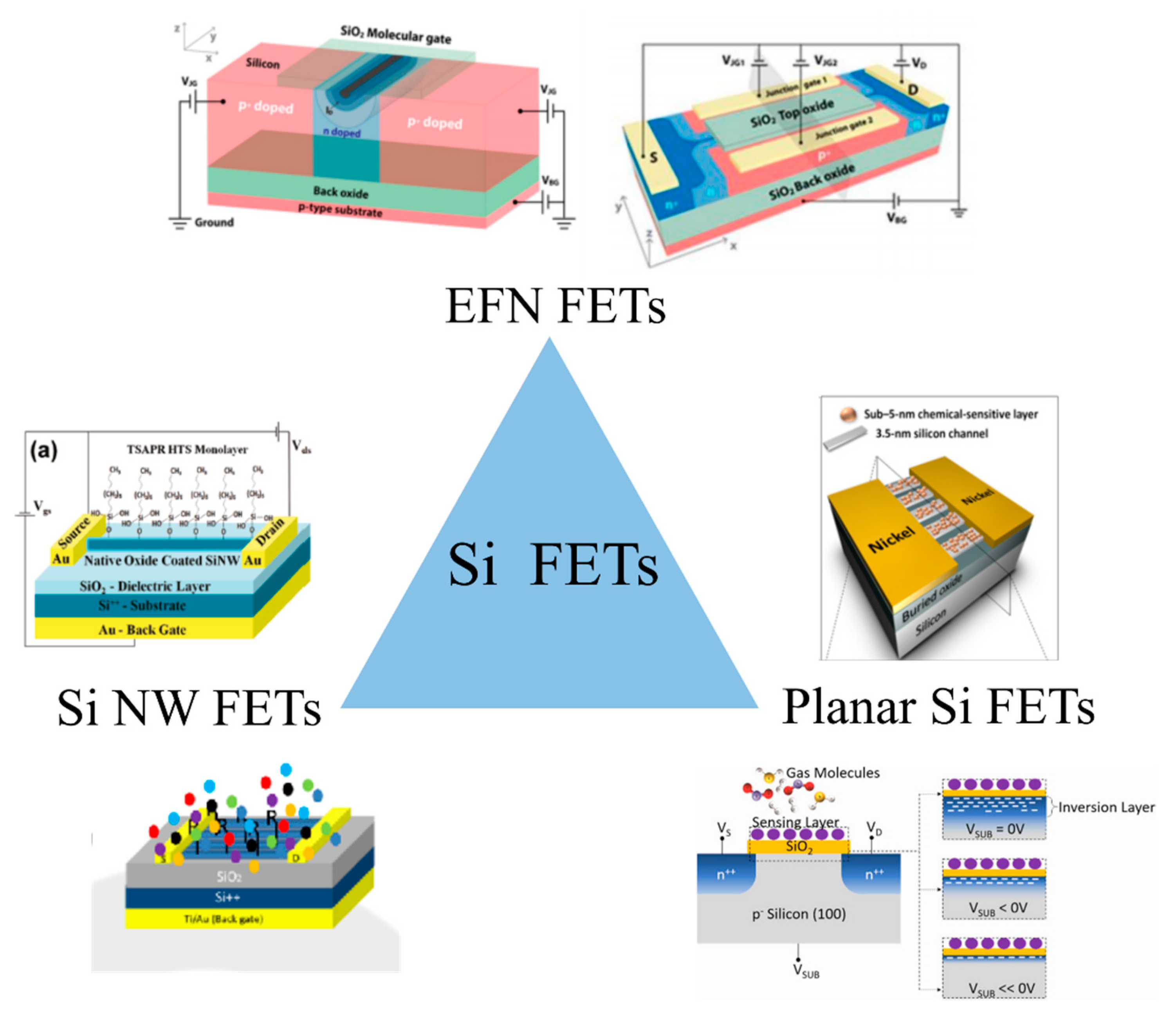
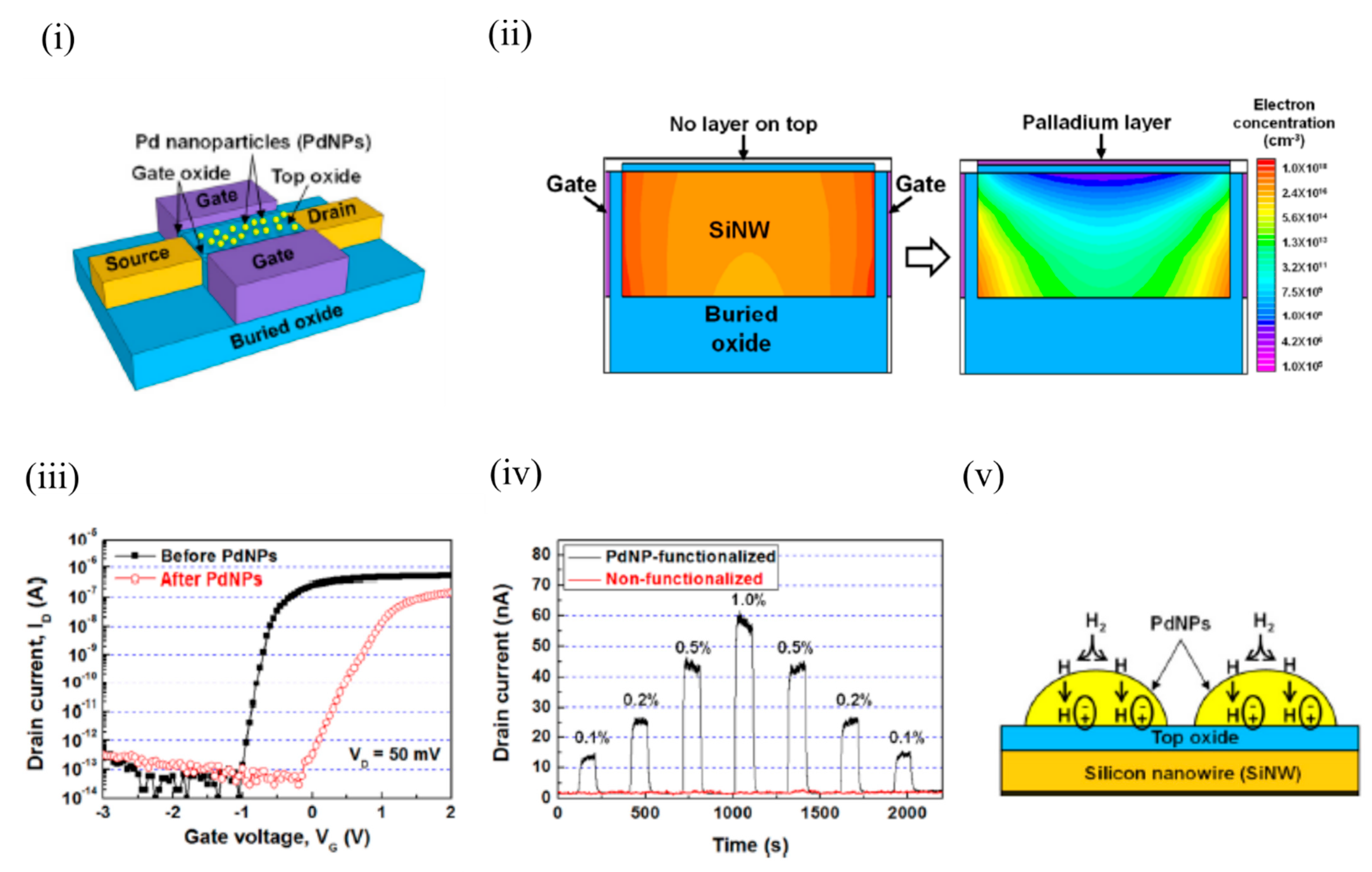
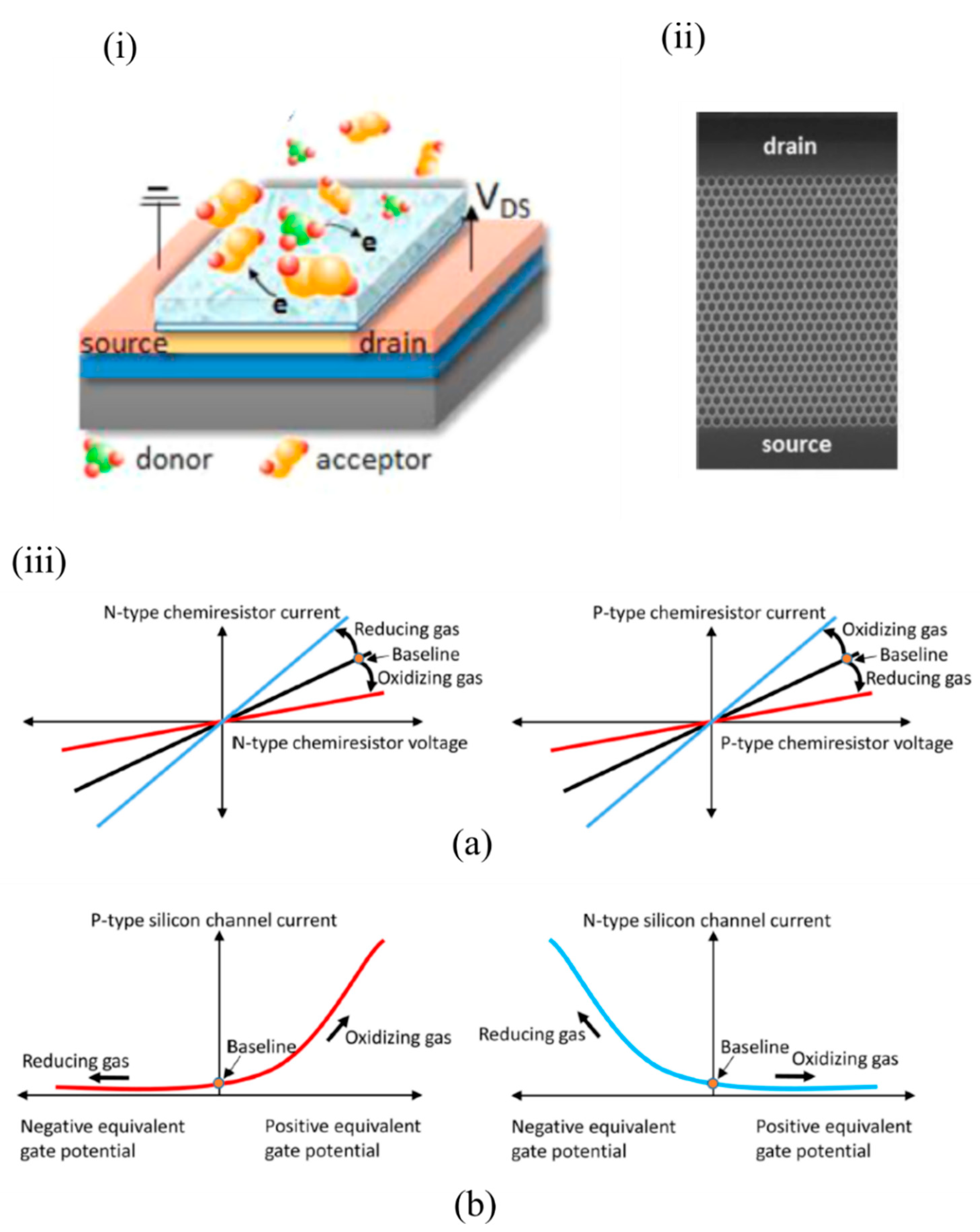
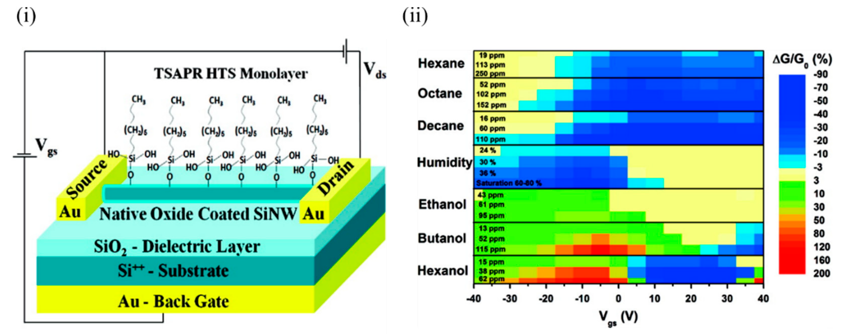
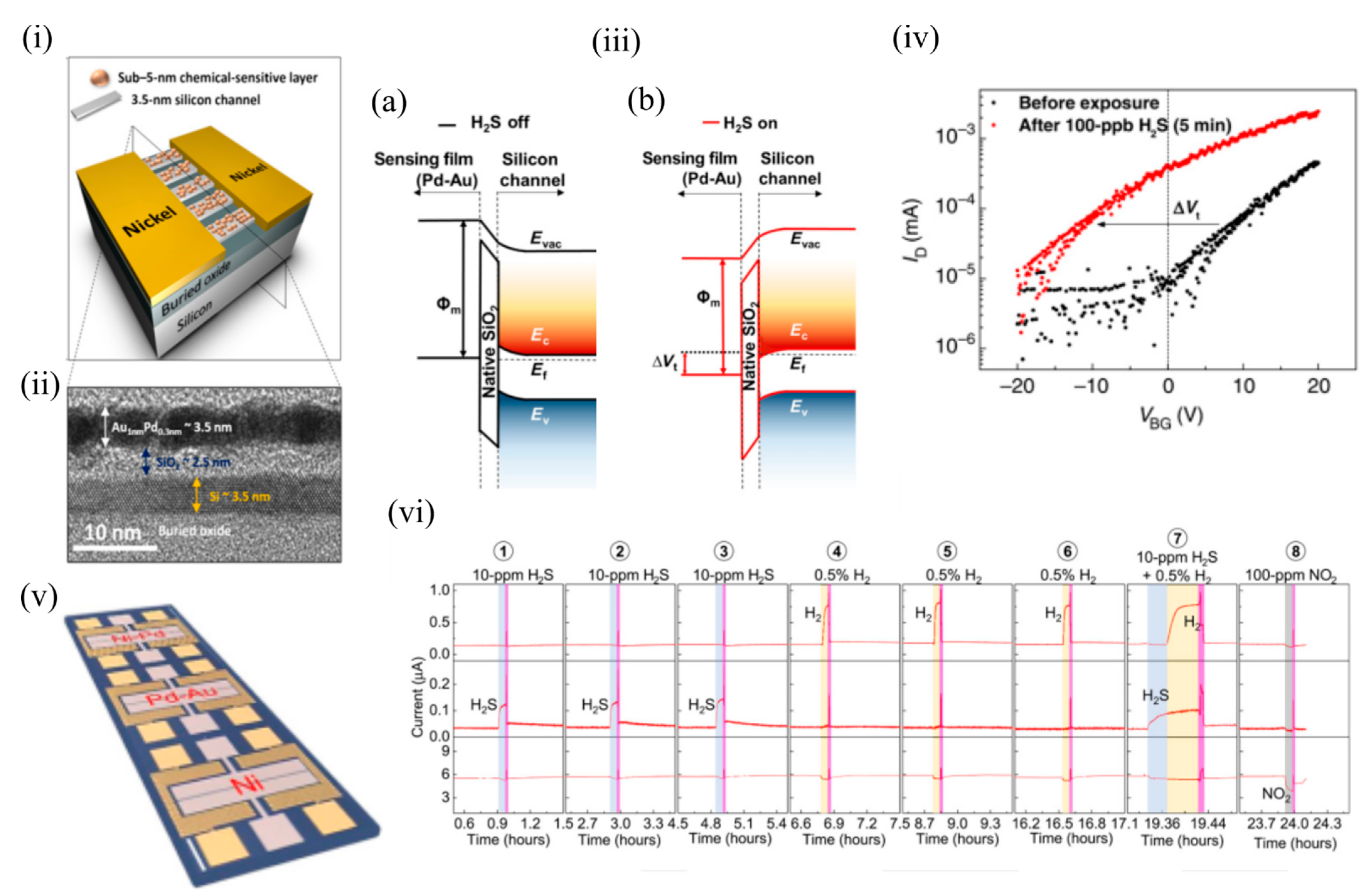
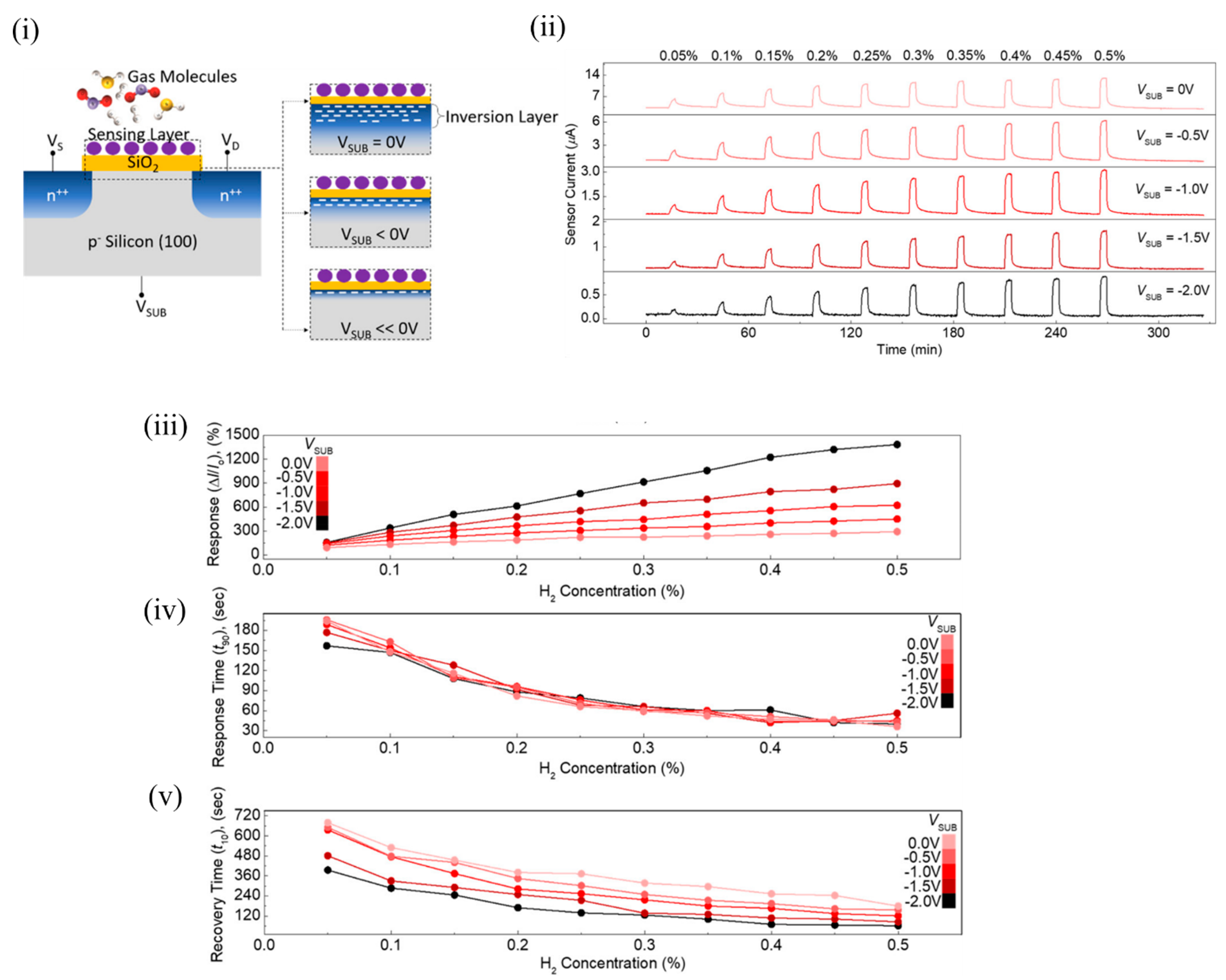
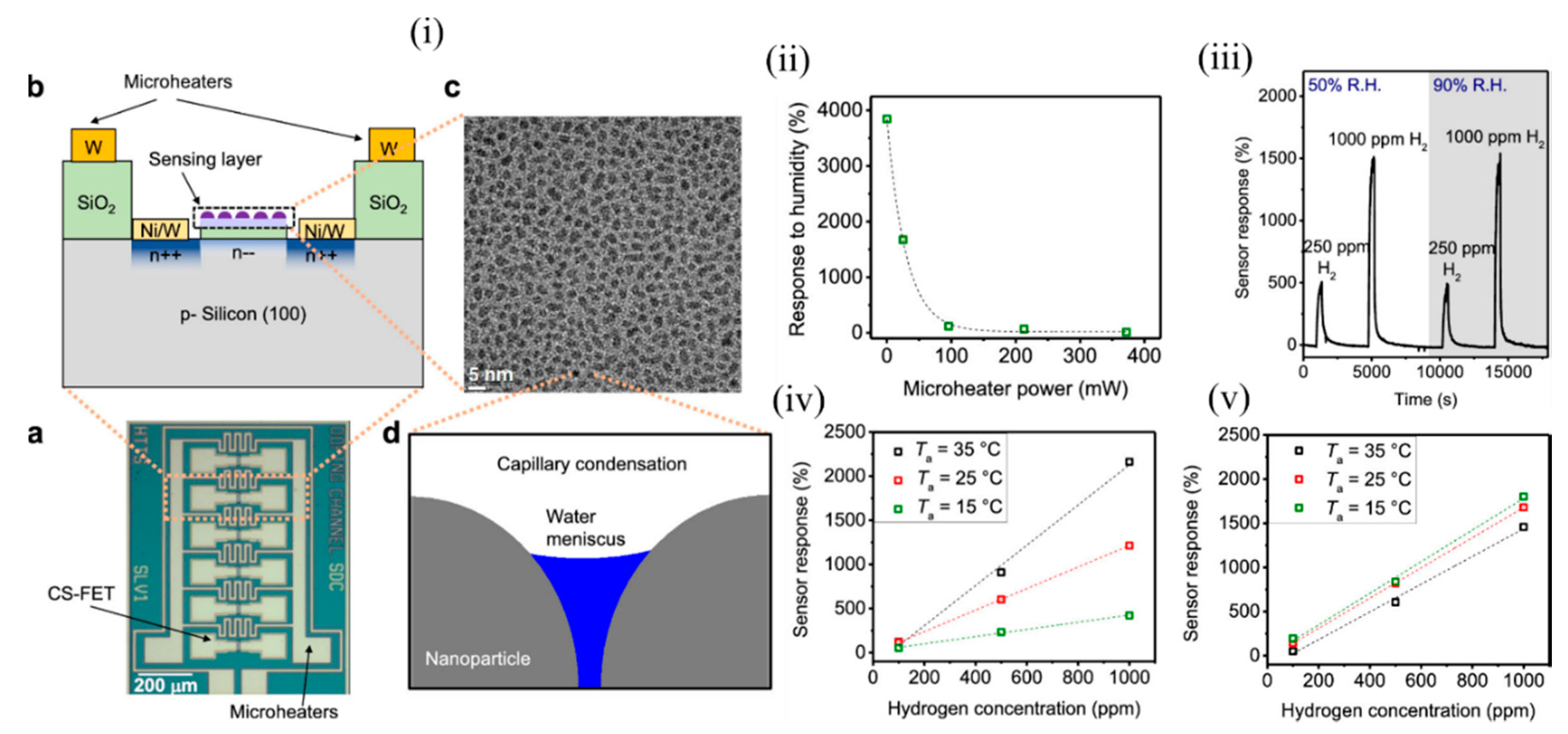
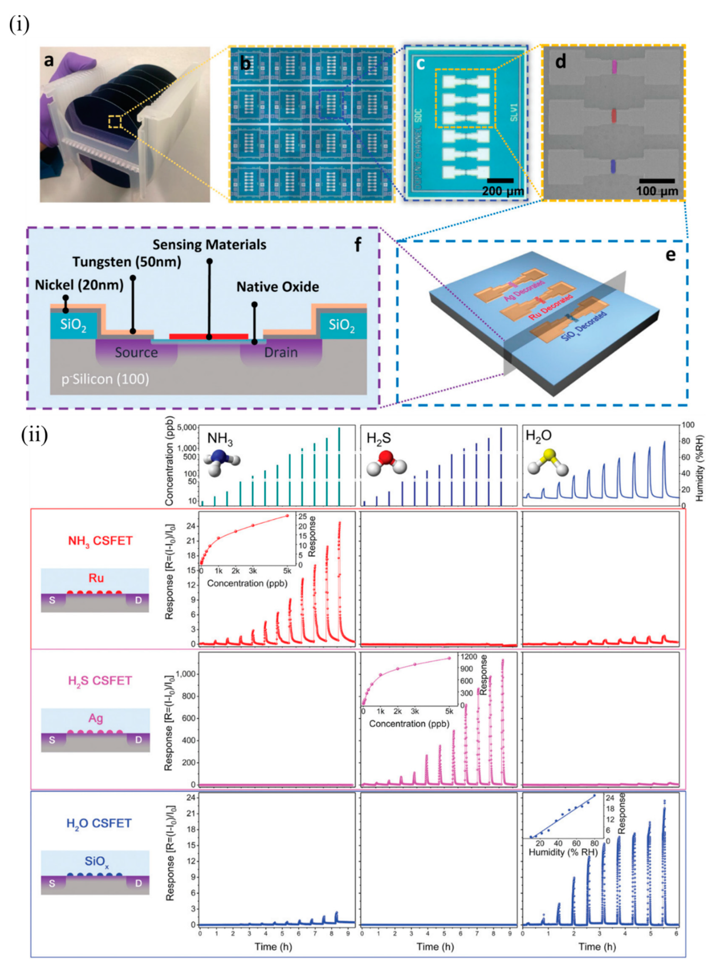
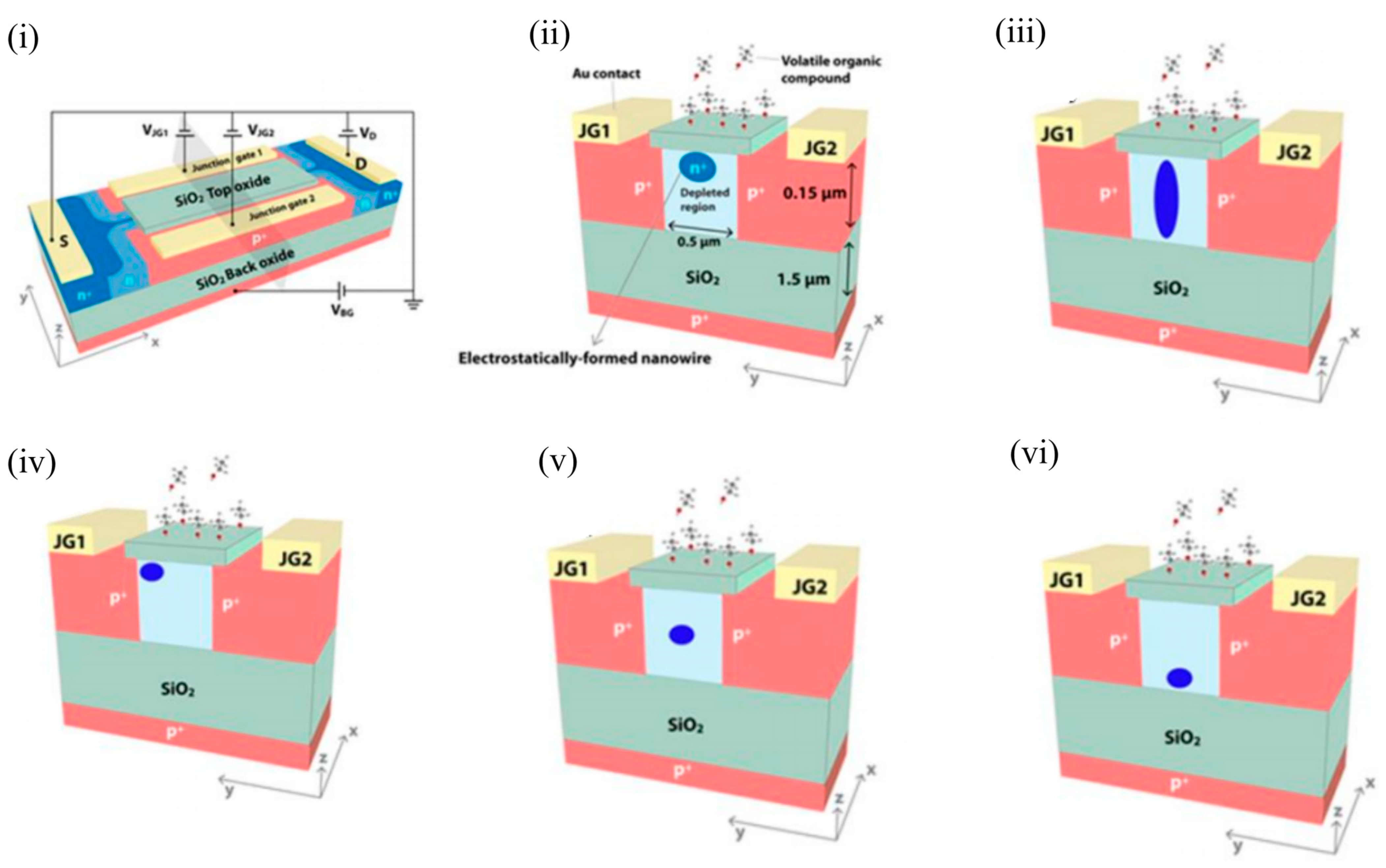
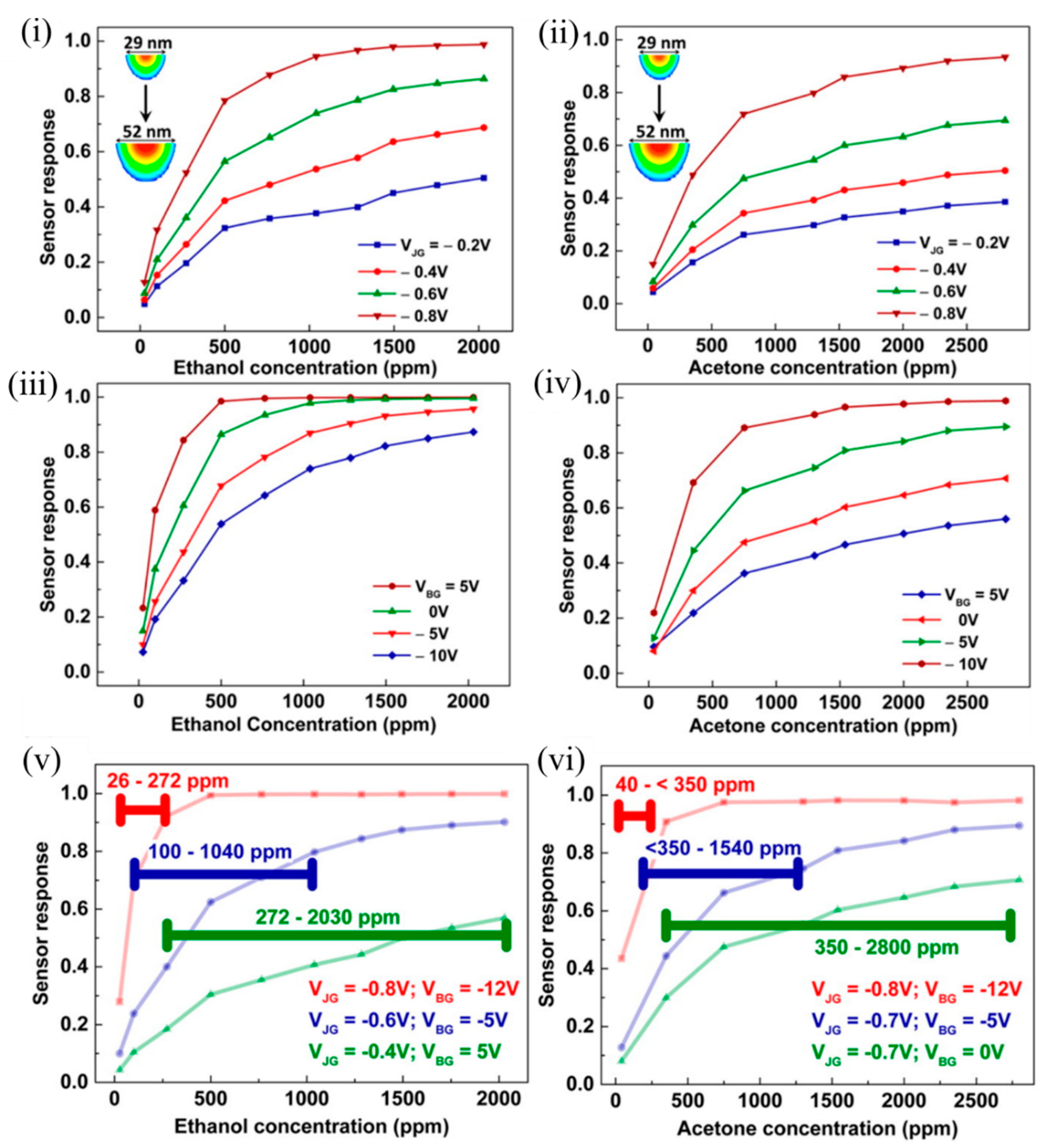
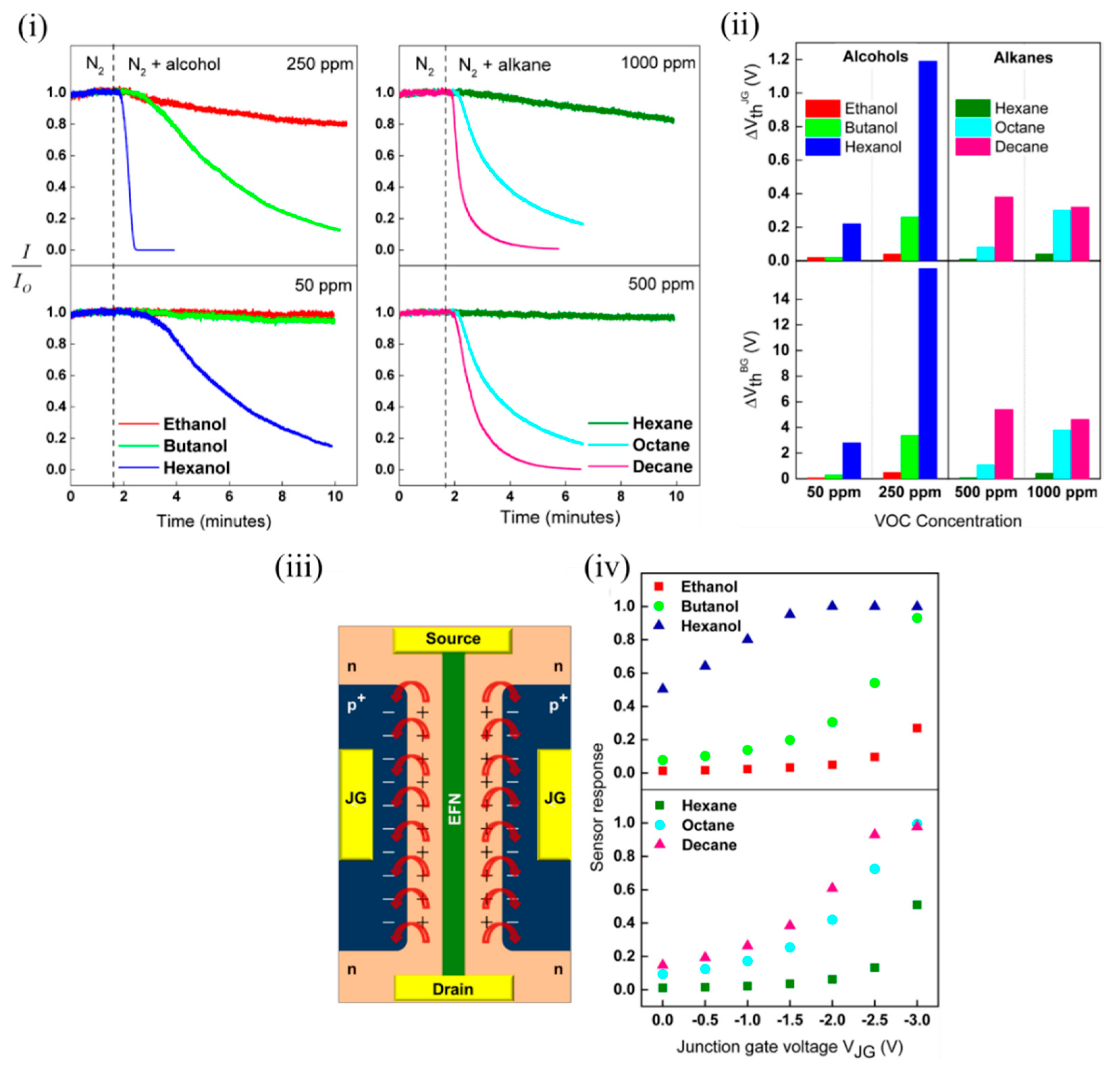
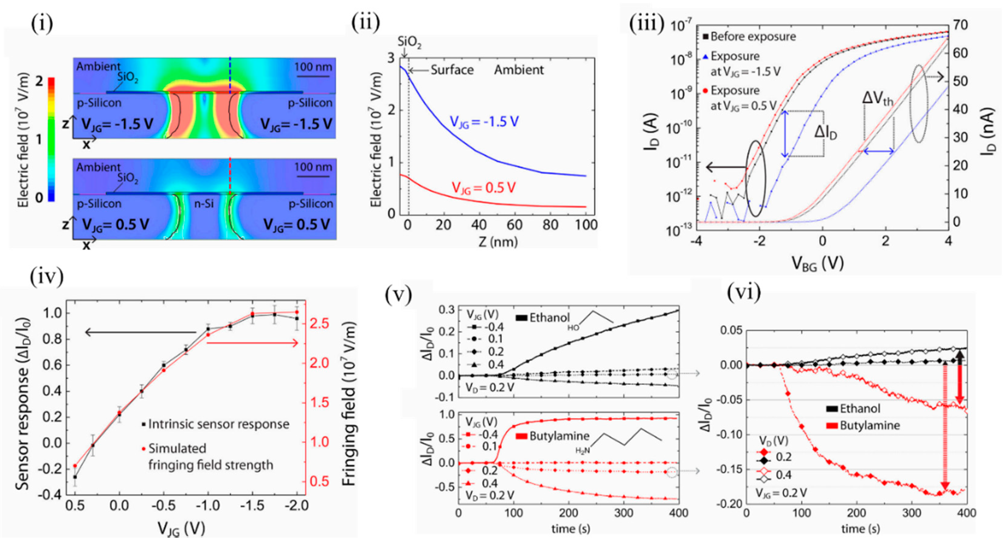
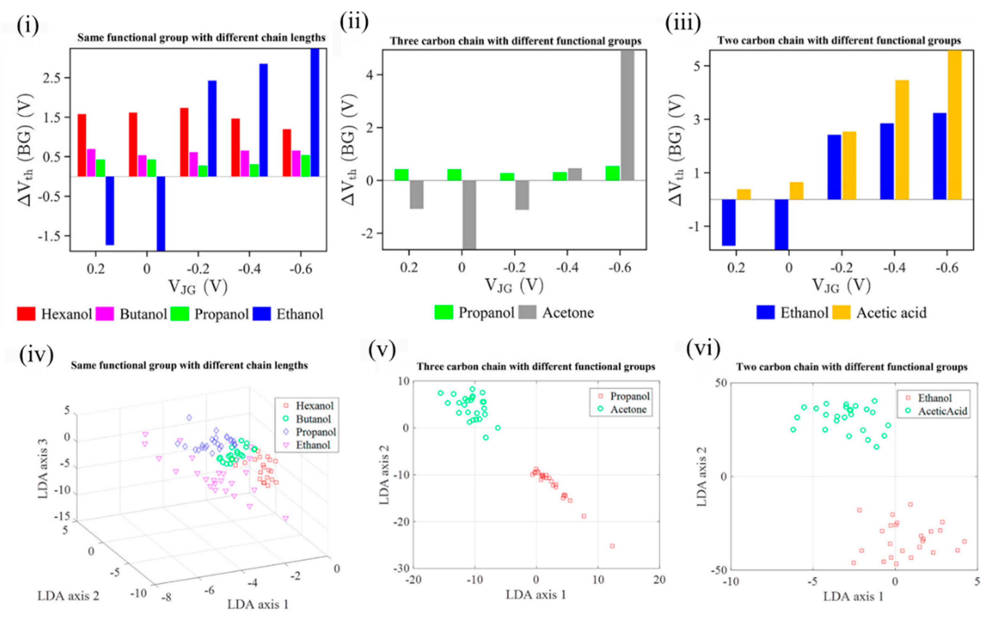
Figure 2.
Pd NP-decorated Si NW FET sensor with local side gates. (i) Schematic of the Pd NP-decorated Si NW FET (fabricated from a SOI substrate using a top-down approach for H2 sensing). The FET architecture involved two side gates apart from a global bottom gate that controlled the working regime of the device from the linear to the subthreshold regime for the sensitivity improvement. (ii) Simulated cross-sectional electron concentration under zero bias of side gates before and after setting the Pd layer (top gate) with a work function of 5 eV on the top surface. (iii) Transfer (ID-VG) characteristics of the device before and after Pd NPs decoration. (iv) Variation in the drain current upon exposure to different concentrations of H2 at various gate voltages. (v) Schematic of the H2 sensing mechanism in the Pd-decorated Si NW FET. The Pd NPs dissociated H2 into hydrogen atoms, which diffused into the Pd NPs and generated hydrogen-induced dipole layers at the interface between the Pd NPs and the top oxide of the Si NW. The positive dipole layers modulated the current flowing through Si NW. Adapted and reprinted from [34] with the permission of AIP Publishing.

Figure 3.
Schematic illustration of (i) metal–oxide (SnO2) floating-gate CGFET. (ii) Scanning electron microscope image of the fabricated SnO2 CGFET. (iii) Representative illustration of the response of (a) the chemiresistor and (b) the CGFET to oxidizing and reducing gases. The monotonic function of the chemiresistor resulted in a response to both oxidizing and reducing gases. The nonlinearity of the normally off CGFET selectively responded to the corresponding type of gas. Adapted and reprinted with permission from [37]. Copyright (2015) American Chemical Society.

Figure 4.
(i) Schematic of a back-gated Si NW FET configuration coated with a 0% cross-linked HTS monolayer. (ii) Counter map of the relative conductivity change of the device at various gate voltages for the polar and nonpolar VOCs at different concentrations. In the case of hexanol, the gate voltage shifted to a lower value, and the relative conductivity change became positive. Adapted and reprinted with permission from [26]. Copyright (2011) American Chemical Society.

Figure 5.
The CS-FET gas sensor. (i) Schematic illustration of a single CS-FET device decorated with NPs. (ii) Cross-sectional TEM image taken across the ultrathin silicon channel as shown in (i). (iii) Schematic illustration of the band edge alignment across the Pd–Au sensing layer and ultrathin Si channel in a H2S-sensitive CS-FET (a) before H2S exposure and (b) after 100 ppb of H2S exposure. Evac, vacuum energy level; Ec, bottom of the Si conduction band energy level; Ev, top of the silicon valence band energy level; Ef, silicon Fermi-level energy. (iv) FET transfer characteristics (ID-VBG) of a H2S-sensitive CS-FET demonstrating Vt shift due to 100-ppb H2S (in air) exposure (VDS = 10 mV). (v) Optical microscopy image of a single CS-FET array chip. Scale bar = 200 μm. (vi) Real-time multiplexed sensing data for different gases (VDS = 25 mV; VBG = 0 V; relative humidity, ~40%; T ≈ 25 °C). Adapted and reprinted from [6] under the Creative Commons Attribution-NonCommercial license.

Figure 6.
The bulk Si-based CS-FET gas sensor. (i) Cross-sectional schematic of a bulk Si CS-FET with electrostatic confinement of the charge inversion layer to achieve high sensitivity. (ii) Variation in sensor current of a Ni–Pd CS-FET when exposed to different H2 concentrations at different body biases (VDS = 3 V, RH < 10%). (iii) Sensor response (ΔI/I0) vs. H2 concentrations, (iv) response time (t90) vs. concentration, and (v) recovery time (t10) vs. concentration from panel (ii) at different VSUB. Reprinted with permission from [24]. Copyright (2018) American Chemical Society.

Figure 7.
The CS-FET gas senor with integrated microheaters. (i) (a) Optical micrograph of the CS-FET chip with the microheaters, and (b) schematic of the cross section. (c) Top-down TEM image of Pt/FOTS on SiO2 grids. (d) Schematic of capillary condensation of water occurring in the cavity between decorated NPs. (ii) Sensor response of the CS-FET to a relative humidity change from 50 to 90% vs. microheater power. (iii) Sensor response to 250 and 1000 ppm of H2 at relative humidity levels (R.H.) of 50 and 90% with VD = 0.65 V, at a chip temperature of 64 ± 8 °C. (iv) Sensor response vs. H2 concentration in different ambient temperatures (Ta) at VD = 0.6 V with microheaters off, and (v) with microheaters on at 372 mW. Adapted and reprinted with permission from [48]. Copyright (2019) American Chemical Society.

Figure 8.
The multi-CS-FET array. (i) Device structure of CS-FETs: (a) photograph of 4 in wafers from which CS-FET arrays were fabricated, and (b) a magnified image of multiple arrays on a single wafer; (c) optical microscope image of a multimaterial-decorated CS-FET array, and (d) a corresponding SEM image with the location of different sensing materials marked in false color; (e) 3D schematic of the multi-CS-FET array, and (f) cross-sectional schematic of the device. (ii) Sensing performance of various NP-decorated CS-FETs. Response of each CS-FET towards different gases with varying concentration (at VDS = 1 V, Vsub = 0 V). Each row in the same color depicts the response curves of the CS-FET indicated on the left (NH3, H2S, and H2O CS-FET, from top to bottom). Each column indicates the response curves towards varying concentrations of the gas indicated at the top (NH3, H2S, and humidity, from left to right). Reproduced with permission from [53]. Copyright (2020) WILEY-VCH.

Figure 9.
Design and various modes of operation of an EFN gas sensor. (i) EFN gas sensor in an electrical biasing configuration. (ii) Small EFN at the top of the bulk SOI: VJG1 = VJG2 < 0 V and VBG < 0 V. (iii) Elongated EFN: VJG1 = VJG2 < 0 V and VBG = 0 V. (iv) Asymmetric biasing configuration—small EFN near to JG1: VJG1 = 0 V, VJG2 < 0 V, and VBG < 0 V. (v) Small EFN in the middle: VJG1 = VJG2 < 0 V and VBG = 0 V. A gradient of donor concentration with a peak at the center of the SOI is required to position the EFN in the middle of the bulk SOI. (vi) Small EFN at the bottom: VJG1 = VJG2 < 0 V and VBG = 0 V. A gradient of donor concentration with a peak at the bottom of the SOI is required to position the EFN in the bottom of the bulk SOI. (i) and (ii) are reprinted from [62], with permission of Tsinghua University Press and Springer-Verlag Berlin Heidelberg, 2015. (iii–vi) are reprinted from [27] with permission to use under the Creative Commons license.

Figure 10.
Sensor responses of the EFN to varying concentrations of ethanol and acetone. Sensor response as a function of VOC concentration measured at (i,ii) different VJG values at VBG = −3 V and (iii,iv) different VBG values at VJG = −0.7 V, for ethanol and acetone, respectively. Sensor response of the EFN device operated at different optimum gate biases to span the proposed dynamic range of (v) ~26–2030 ppm for ethanol, and (vi) ~40–2800 ppm for acetone. The horizontal lines indicate the calculated dynamic range for the particular EFN configuration such that the sensor response was ≥0.2 throughout. Reprinted with permission from [67]. Copyright (2016) American Chemical Society.

Figure 11.
EFN sensor for sensing polar alcohols and nonpolar alkanes. (i) Plot of normalized sensor response of the EFN vs. time for alcohols (left) and alkanes (right). (ii) Plot of shift in threshold voltage of the EFN sensor with respect to the junction gate (top) and back gate (below) at two different concentrations of alcohols (50 and 250 ppm) (left) and alkanes (500 and 1000 ppm) (right). (iii) Schematic top view of the EFN sensor depicting the two back-to-back p-n regions on either side of the channel marked with ‘+’ and ‘−’ (the top oxide is not shown for clarity). The red arrows indicate the fringing fields due to the induced electric fields in the space charge region. (iv) Plot of sensor response to alcohols (top) and alkanes (bottom) vs. the applied junction gate voltage of the EFN. Adapted and reprinted with permission from [70]. Copyright (2017) Elsevier.

Figure 12.
Induced fringing electric field on the surface of the EFN as a tool for selectivity between VOCs. (i) The electric field distributions at the cross sections (x–z planes) of the 3D-modeled EFN device at VJG = −1.5 V (top) and VJG = 0.5 V (bottom) with other electrodes as grounded. (ii) Decaying of the simulated electric field strength with the distance from the sensor surface (Z-axis) above the p–n junction of the EFN device, indicated by the dashed lines in (i). (iii) ID–VBG characteristics in nitrogen before ethanol exposure (black) and after ethanol exposure at VJG = −1.5 V (blue), and VJG = 0.5 V (red) after saturation in sensing had been reached. (iv) Plots of the sensor response: ΔID/I0, (black) and the simulated fringing field maxima (red) as a function of VJG. (v) Plot of sensor response vs. time for exposure to 1500 ppm concentrations of ethanol (top) and n-butylamine (bottom) vapors at four different VJGs, and at constant VD = 0.2 V and VBG = −20 V. (vi) Comparison of the sensor responses between ethanol and n-butylamine at VD = 0.2 V and VD = 0.4 V, at constant VJG = 0.2 V and VBG = −20 V, indicating selectivity at definite working voltages. Reprinted with permission from [72]. Copyright (2018) American Chemical Society.

Figure 13.
EFN as a versatile platform for obtaining electrostatic selectivity against targeted VOCs. Changes in Vth (BG) at different VJG of the EFN sensor at a fixed VDS = 0.4 V, upon exposure to (i) four homologous alcohols (hexanol, butanol, propanol, and ethanol), (ii) propanol and acetone, and (iii) ethanol and acetic acid. The concentrations used for hexanol, butanol, propanol, ethanol, acetone, and acetic acid were 200 ppm (8.8 μM), 1000 ppm (44 μM), 1700 ppm (74 μM), 1800 ppm (79 μM), 3000 ppm (132 μM), and 8800 ppm (387 μM), respectively. The first three LDA axes of observations were taken from (iv) four homologous alcohols (hexanol, butanol, propanol, and ethanol). The first two LDA axes of observations were taken from (v) propanol and acetone and (vi) ethanol and acetic acid. The homologous alcohols showed poor separability in the LDA analysis, and various machine-learning classifiers were employed to distinguish them. Adapted and reprinted with permission from [63]. Copyright (2018) American Chemical Society.

Publisher’s Note: MDPI stays neutral with regard to jurisdictional claims in published maps and institutional affiliations. |
© 2021 by the authors. Licensee MDPI, Basel, Switzerland. This article is an open access article distributed under the terms and conditions of the Creative Commons Attribution (CC BY) license (https://creativecommons.org/licenses/by/4.0/).
Share and Cite
MDPI and ACS Style
Mukherjee, A.; Rosenwaks, Y. Recent Advances in Silicon FET Devices for Gas and Volatile Organic Compound Sensing. Chemosensors 2021, 9, 260. https://0-doi-org.brum.beds.ac.uk/10.3390/chemosensors9090260
AMA Style
Mukherjee A, Rosenwaks Y. Recent Advances in Silicon FET Devices for Gas and Volatile Organic Compound Sensing. Chemosensors. 2021; 9(9):260. https://0-doi-org.brum.beds.ac.uk/10.3390/chemosensors9090260
Chicago/Turabian StyleMukherjee, Anwesha, and Yossi Rosenwaks. 2021. "Recent Advances in Silicon FET Devices for Gas and Volatile Organic Compound Sensing" Chemosensors 9, no. 9: 260. https://0-doi-org.brum.beds.ac.uk/10.3390/chemosensors9090260
Note that from the first issue of 2016, this journal uses article numbers instead of page numbers. See further details here.