Single-Objective Optimization of a CMOS VCO Considering PVT and Monte Carlo Simulations


Abstract
:1. Introduction
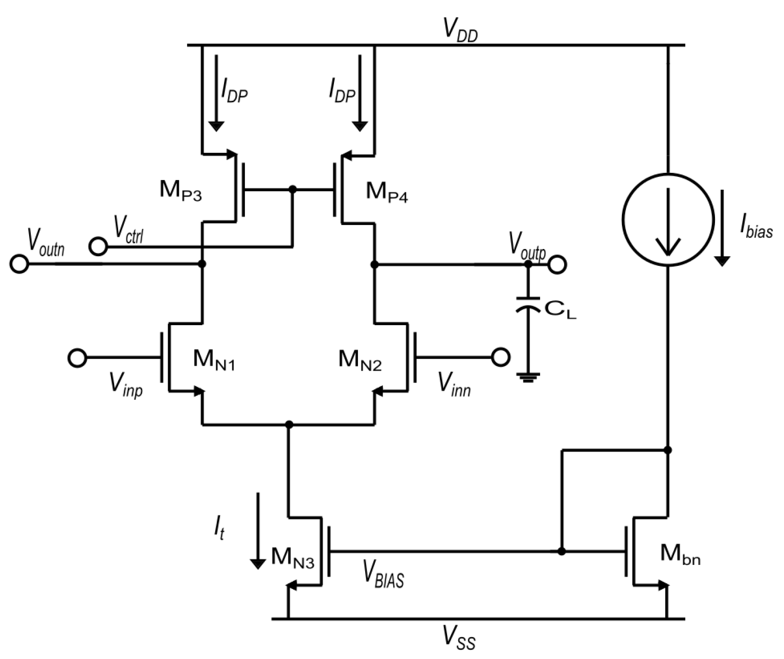
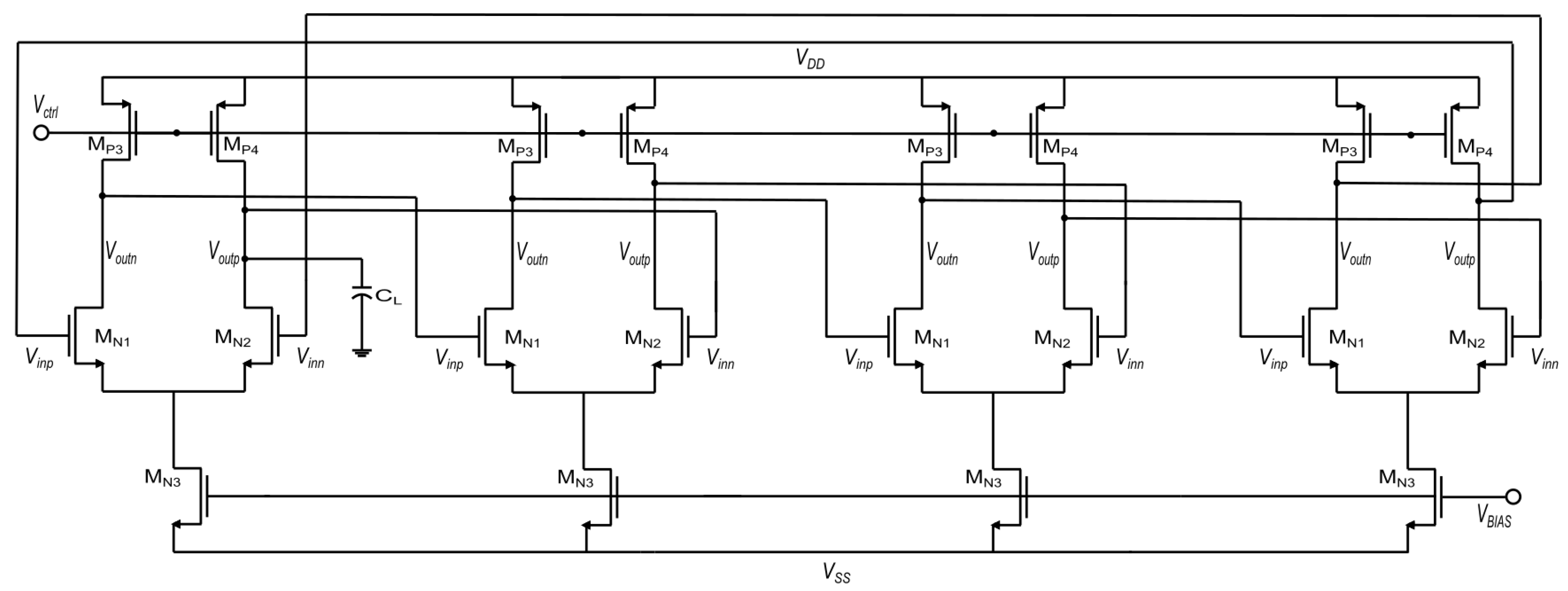
2. Ring VCO-Based on CMOS Differential Stages
3. VCO Optimization Methods
4. Problem Formulation for the Optimization of the VCO by Applying DE
| Algorithm 1 DE pseudocode. |
|
5. Optimizing the CMOS VCO by Applying DE Algorithm
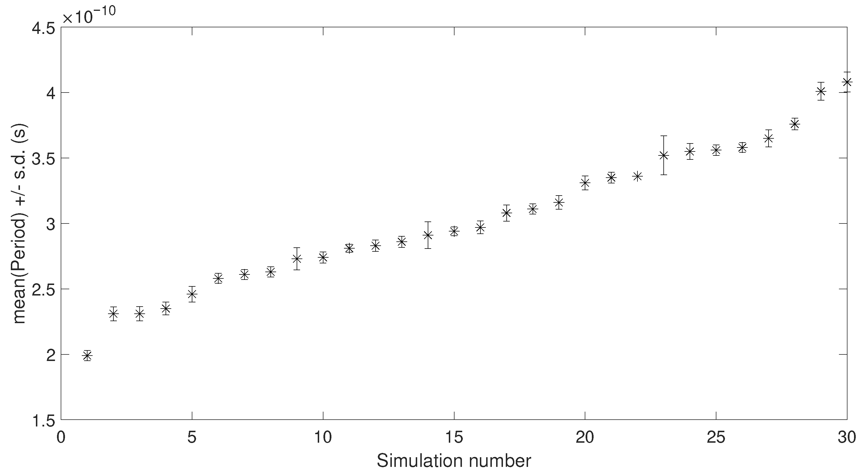
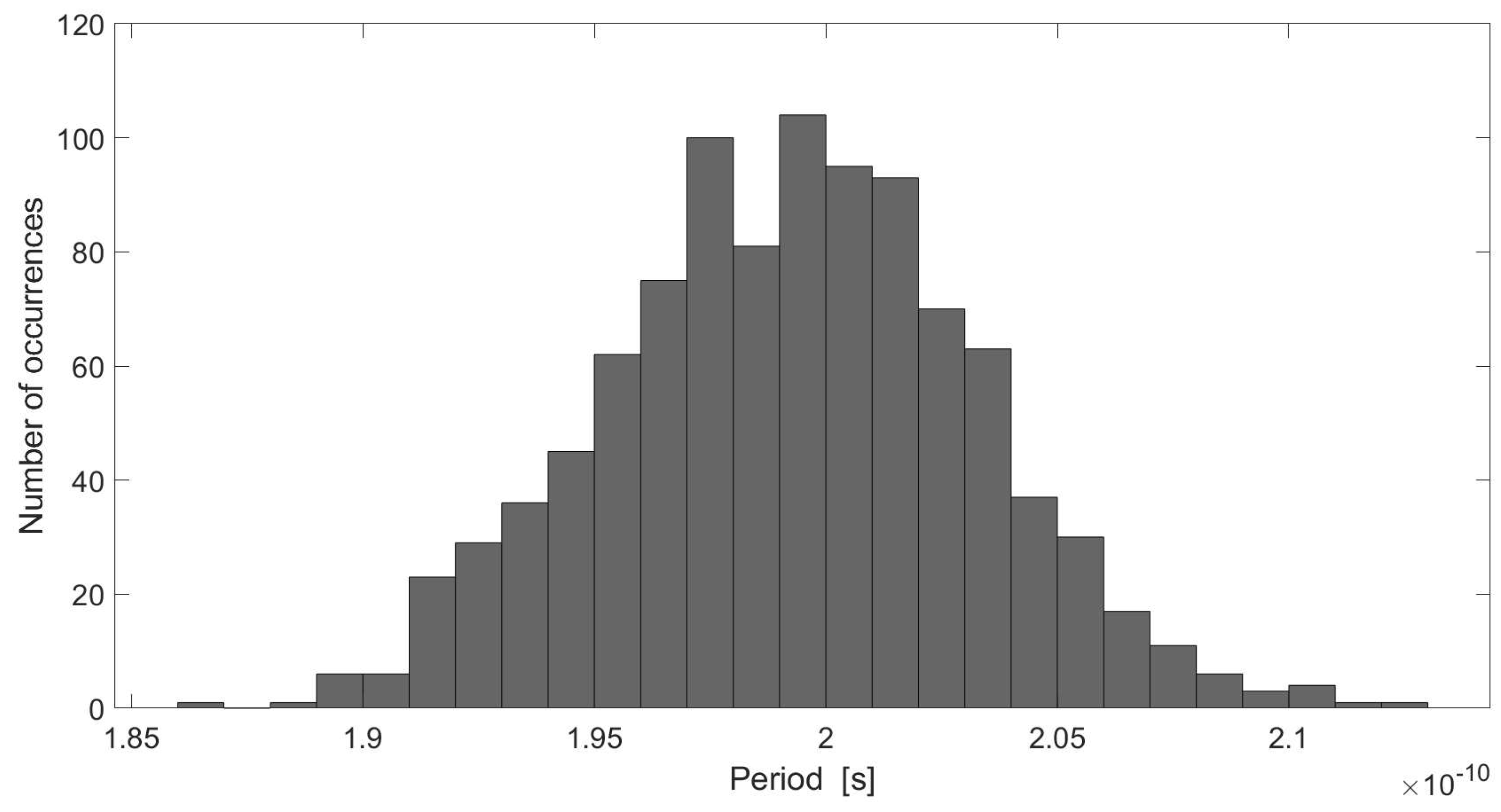
6. Discussion
7. Conclusions
Author Contributions
Funding
Conflicts of Interest
References
- Al-Tamimi, K.M.; El-Sankary, K.; Fouzar, Y. VCO-Based ADC With Built-In Supply Noise Immunity Using Injection-Locked Ring Oscillators. IEEE Trans. Circuits Syst. Express Briefs 2019, 66, 1089–1093. [Google Scholar] [CrossRef]
- Ding, Z.; Zhou, X.; Li, Q. A 0.5-1.1-V Adaptive Bypassing SAR ADC Utilizing the Oscillation-Cycle Information of a VCO-Based Comparator. IEEE J. Solid State Circuits 2019, 54, 968–977. [Google Scholar] [CrossRef]
- Danesh, M.; Sanyal, A. 0.13 pW/Hz Ring VCO-Based Continuous-Time Read-Out ADC for Bio-Impedance Measurement. IEEE Trans. Circuits Syst. II Express Briefs 2020. [Google Scholar] [CrossRef]
- Sharma, J.; Krishnaswamy, H. A 2.4-GHz Reference-Sampling Phase-Locked Loop That Simultaneously Achieves Low-Noise and Low-Spur Performance. IEEE J. Solid State Circuits 2019, 54, 1407–1424. [Google Scholar] [CrossRef]
- Tlelo-Cuautle, E.; Castañeda-Aviña, P.R.; Trejo-Guerra, R.; Carbajal-Gómez, V.H. Design of a Wide-Band Voltage-Controlled Ring Oscillator Implemented in 180 nm CMOS Technology. Electronics 2019, 8, 1156. [Google Scholar] [CrossRef] [Green Version]
- Lee, I.Y.; Im, D. Low phase noise ring VCO employing input-coupled dynamic current source. Electron. Lett. 2019, 56, 76–78. [Google Scholar] [CrossRef]
- Panda, M.; Patnaik, S.K.; Mal, A.K. Performance enhancement of a VCO using symbolic modelling and optimisation. IET Circuits Devices Syst. 2017, 12, 196–202. [Google Scholar] [CrossRef]
- Gui, X.; Tang, R.; Zhang, Y.; Li, D.; Geng, L. A Voltage-Controlled Ring Oscillator With VCO-Gain Variation Compensation. IEEE Microw. Wirel. Components Lett. 2020, 30, 288–291. [Google Scholar] [CrossRef]
- Jung, O.Y.; Seok, H.G.; Dissanayake, A.; Lee, S.G. A 45-μ W, 162.1-dBc/Hz FoM, 490-MHz Two-Stage Differential Ring VCO Without a Cross-Coupled Latch. IEEE Trans. Circuits Syst. II Express Briefs 2017, 65, 1579–1583. [Google Scholar] [CrossRef]
- Jiang, T.; Yin, J.; Mak, P.I.; Martins, R.P. A 0.5-V 0.4-to-1.6-GHz 8-phase bootstrap ring-VCO using inherent non-overlapping clocks achieving a 162.2-dBc/Hz FoM. IEEE Trans. Circuits Syst. II Express Briefs 2018, 66, 157–161. [Google Scholar] [CrossRef]
- Sun, I.F.; Yin, J.; Mak, P.I.; Martins, R.P. A Comparative Study of 8-Phase Feedforward-Coupling Ring VCOs. IEEE Trans. Circuits Syst. II Express Briefs 2019, 66, 527–531. [Google Scholar] [CrossRef]
- Abidi, A.A. Phase noise and jitter in CMOS ring oscillators. IEEE J. Solid State Circuits 2006, 41, 1803–1816. [Google Scholar] [CrossRef]
- Gui, X.; Green, M.M. Design of CML ring oscillators with low supply sensitivity. IEEE Trans. Circuits Syst. Regul. Pap. 2013, 60, 1753–1763. [Google Scholar] [CrossRef]
- Zhang, Z.; Chen, L.; Djahanshahi, H. A SEE Insensitive CML Voltage Controlled Oscillator in 65 nm CMOS. In Proceedings of the 2018 IEEE Canadian Conference on Electrical & Computer Engineering (CCECE), Quebec City, QC, Canada, 13–16 May 2018; pp. 1–4. [Google Scholar] [CrossRef]
- Amaya, A.; Villota, F.; Espinosa, G. A robust to PVT fully-differential amplifier in 45 nm SOI-CMOS technology. In Proceedings of the 2013 IEEE 4th Latin American Symposium on Circuits and Systems (LASCAS), Cusco, Peru, 27 February–1 March 2013; pp. 1–4. [Google Scholar]
- Hsieh, J.Y.; Lin, K.Y. A 0.7-mW LC Voltage-Controlled Oscillator Leveraging Switched Biasing Technique for Low Phase Noise. IEEE Trans. Circuits Syst. II Express Briefs 2019, 66, 1307–1310. [Google Scholar] [CrossRef]
- Basaligheh, A.; Saffari, P.; Winkler, W.; Moez, K. A Wide Tuning Range, Low Phase Noise, and Area Efficient Dual-Band Millimeter-Wave CMOS VCO Based on Switching Cores. IEEE Trans. Circuits Syst. I Regul. Pap. 2019, 66, 2888–2897. [Google Scholar] [CrossRef]
- Poor, M.A.; Esmaeeli, O.; Sheikhaei, S. A low phase noise quadrature VCO using superharmonic injection, current reuse, and negative resistance techniques in CMOS technology. Analog. Integr. Circuits Signal Process. 2019, 99, 633–644. [Google Scholar] [CrossRef]
- Ghorbel, I.; Haddad, F.; Rahajandraibe, W.; Loulou, M. Design Methodology of Ultra-Low-Power LC-VCOs for IoT Applications. J. Circuits Syst. Comput. 2019, 28. [Google Scholar] [CrossRef]
- De Melo, J.L.; Pereira, N.; Leitão, P.V.; Paulino, N.; Goes, J. A Systematic Design Methodology for Optimization of Sigma-Delta Modulators Based on an Evolutionary Algorithm. IEEE Trans. Circuits Syst. I Regul. Pap. 2019, 66, 3544–3556. [Google Scholar] [CrossRef]
- Vural, R.A.; Yildirim, T.; Kadioglu, T.; Basargan, A. Performance evaluation of evolutionary algorithms for optimal filter design. IEEE Trans. Evol. Comput. 2011, 16, 135–147. [Google Scholar] [CrossRef]
- Panda, M.; Patnaik, S.K.; Mal, A.K.; Ghosh, S. Fast and optimised design of a differential VCO using symbolic technique and multi objective algorithms. IET Circuits Devices Syst. 2019, 13, 1187–1195. [Google Scholar] [CrossRef]
- Heydari, P.; Mohanavelu, R. Design of ultrahigh-speed low-voltage CMOS CML buffers and latches. IEEE Trans. Very Large Scale Integr. (VLSI) Syst. 2004, 12, 1081–1093. [Google Scholar] [CrossRef] [Green Version]
- Kumar, M. Design of Linear Low-Power Voltage-Controlled Oscillator with I-MOS Varactor and Back-Gate Tuning. Circuits Syst. Signal Process. 2018, 1–17. [Google Scholar] [CrossRef]
- Sedra, A.S.; Smith, K.C. Microelectronic Circuits; Holt, Rinehart and Winston: New York, NY, USA, 1982. [Google Scholar]
- Jyotsna, K.; Kumar, P.S.; Madhavi, B. Implementation of 8 Bit Microprocessor Using Current Mode Logic (CML) Approach. In Proceedings of the 2018 3rd International Conference for Convergence in Technology (I2CT), Pune, India, 6–8 April 2018; pp. 1–6. [Google Scholar] [CrossRef]
- Palumbo, G.; Pennisi, S. Feedback Amplifiers: Theory and Design; Springer: Berlin/Heisenberg, Germany, 2002. [Google Scholar]
- Maloberti, F. Analog Design for CMOS VLSI Systems; Springer: Berlin/Heisenberg, Germany, 2006; Volume 646. [Google Scholar] [CrossRef] [Green Version]
- Afacan, E.; Dündar, G. A mixed domain sizing approach for RF circuit synthesis. In Proceedings of the 2016 IEEE 19th International Symposium on Design and Diagnostics of Electronic Circuits & Systems (DDECS), Kosice, Slovakia, 20–22 April 2016; pp. 1–4. [Google Scholar]
- Póvoa, R.; Lourenço, R.; Lourenço, N.; Canelas, A.; Martins, R.; Horta, N. LC-VCO automatic synthesis using multi-objective evolutionary techniques. In Proceedings of the 2014 IEEE International Symposium on Circuits and Systems (ISCAS), Victoria, Australia, 1–5 June 2014; pp. 293–296. [Google Scholar]
- Passos, F.; Martins, R.; Lourenço, N.; Roca, E.; Povoa, R.; Canelas, A.; Castro-López, R.; Horta, N.; Fernández, F.V. Enhanced systematic design of a voltage controlled oscillator using a two-step optimization methodology. Integration 2018, 63, 351–361. [Google Scholar] [CrossRef] [Green Version]
- Yang, X.S. Engineering Optimization: An Introduction with Metaheuristic Applications; John Wiley & Sons: Hoboken, NJ, USA, 2010. [Google Scholar] [CrossRef]
- Talbi, E.G. Metaheuristics: From Design to Implementation; John Wiley & Sons: Hoboken, NJ, USA, 2009; Volume 74. [Google Scholar] [CrossRef]
- Dasgupta, D.; Michalewicz, Z. Evolutionary algorithms—An overview. In Evolutionary Algorithms in Engineering Applications; Springer: Berlin/Heisenberg, Germany, 1997; pp. 3–28. [Google Scholar] [CrossRef]
- Coello, C.A.C. An introduction to evolutionary algorithms and their applications. In International Symposium and School on Advancex Distributed Systems; Springer: Berlin/Heisenberg, Germany, 2005; pp. 425–442. [Google Scholar] [CrossRef]
- Woldesenbet, Y.G.; Yen, G.G.; Tessema, B.G. Constraint handling in multiobjective evolutionary optimization. IEEE Trans. Evol. Comput. 2009, 13, 514–525. [Google Scholar] [CrossRef]
- Yu, X.; Gen, M. Introduction to Evolutionary Algorithms; Springer: Berlin/Heisenberg, Germany, 2010. [Google Scholar] [CrossRef]
- Elhajjami, I.; Benhala, B.; Bouyghf, H. Optimal Design of RF Integrated Inductors via Differential Evolution Algorithm. In Proceedings of the 2020 1st International Conference on Innovative Research in Applied Science, Engineering and Technology (IRASET), Meknes, Morocco, 16–19 April 2020; pp. 1–6. [Google Scholar] [CrossRef]
- Li, J.; Zeng, Y.; Wu, H.; Li, R.; Zhang, J.; Tan, H.Z. Performance optimization for LDO regulator based on the differential evolution. In Proceedings of the 2019 IEEE 13th International Conference on ASIC (ASICON), Chongqing, China, 29 October–1 November 2019; pp. 1–4. [Google Scholar] [CrossRef]
- Barik, C.K.; Baksi, R.; Shekhar, H.; Kuanr, B.R.; Lata, M. Effect of parameter tuning of differential evolution on PID controller for automatic generation control of a hybrid power system in deregulated environment. In Proceedings of the 2016 International Conference on Circuit, Power and Computing Technologies (ICCPCT), Nagercoil, India, 18–19 March 2016; pp. 1–6. [Google Scholar] [CrossRef]
- Chen, P.; Cheng, H.C.; Widodo, A.; Tsai, W.X. A PVT insensitive field programmable gate array time-to-digital converter. In Proceedings of the 2013 IEEE Nordic-Mediterranean Workshop on Time-to-Digital Converters (NoMe TDC), Perugia, Italy, 3 October 2013; pp. 1–4. [Google Scholar] [CrossRef]


| Solution | Minimum (ns) | Maximum (ns) | Mean (ns) | Variance | Standard Deviation |
|---|---|---|---|---|---|
| 1 | 0.187 | 0.213 | 0.199 | ||
| 2 | 0.214 | 0.248 | 0.231 | ||
| 3 | 0.214 | 0.249 | 0.231 | ||
| 4 | 0.219 | 0.251 | 0.235 | ||
| 5 | 0.226 | 0.265 | 0.246 |
| Solution | Period (ns) | Frequency (GHz) | |||||||
|---|---|---|---|---|---|---|---|---|---|
| 1 | 40 | 17 | 0.18 | 0.18 | −0.80 | 31.39 | 0.199 | 5.02 | 1.89 |
| 2 | 45 | 20 | 0.18 | 0.18 | −0.56 | 35.22 | 0.232 | 4.32 | 3.39 |
| 3 | 61 | 26 | 0.18 | 0.18 | −0.56 | 54.69 | 0.232 | 4.30 | 1.78 |
| 4 | 69 | 22 | 0.18 | 0.18 | −0.79 | 96.17 | 0.235 | 4.25 | 2.26 |
| 5 | 46 | 20 | 0.18 | 0.18 | −0.51 | 36.19 | 0.246 | 4.07 | 4.41 |
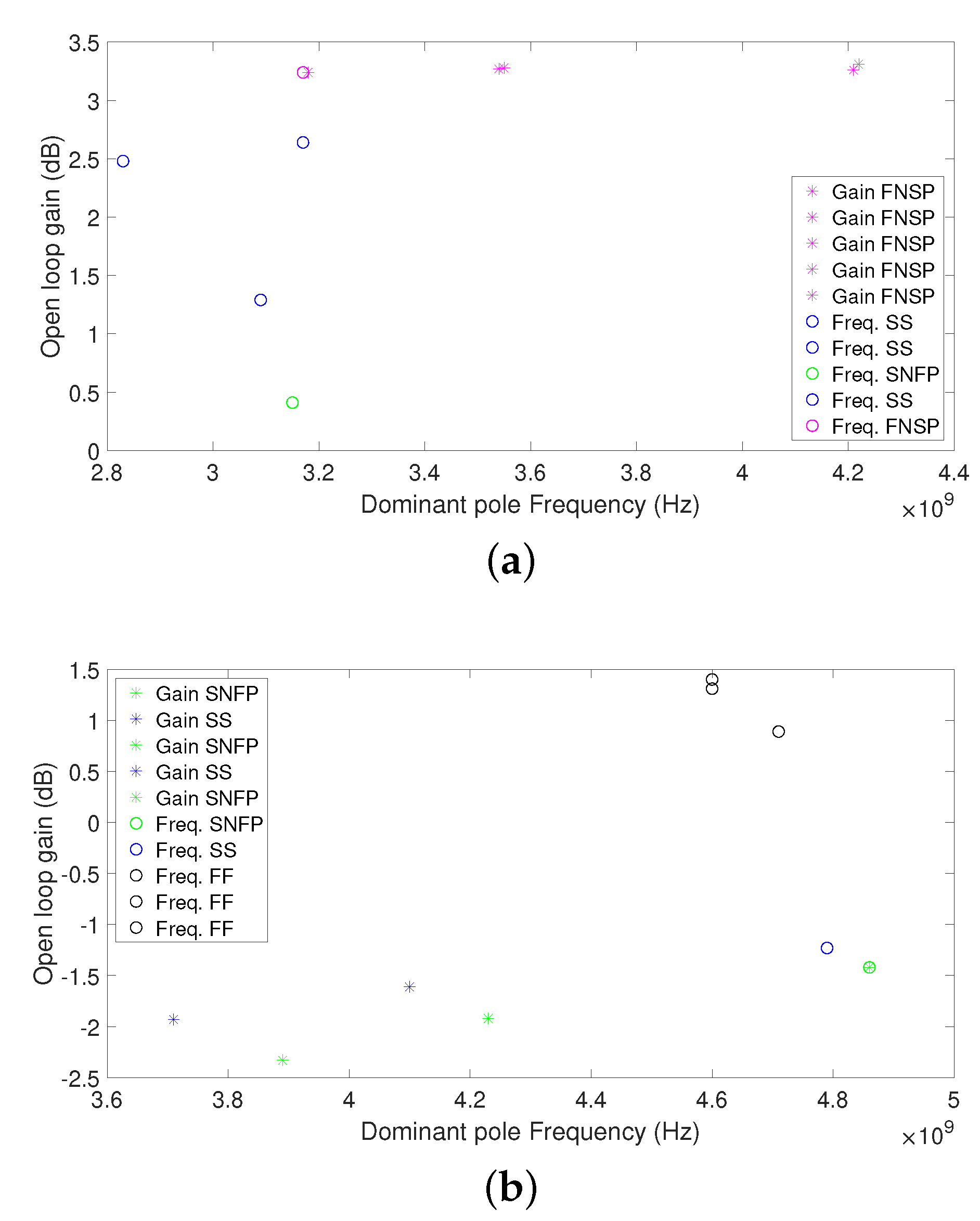
| Solution | Corners | Temperature | T− | T | T+ | ||||||
|---|---|---|---|---|---|---|---|---|---|---|---|
| Voltage | V− | V | V+ | V− | V | V+ | V− | V | V+ | ||
| 1 | TT | (dB) | 0.82 | 1.88 | 2.06 | 0.55 | 1.74 | 1.89 | 0.24 | 1.61 | 1.78 |
| (GHz) | 4.54 | 4.24 | 4.21 | 3.90 | 3.58 | 3.56 | 3.58 | 3.22 | 3.19 | ||
| SS | (dB) | −1.23 | 2.17 | 2.81 | −1.61 | 1.76 | 2.64 | −1.93 | 1.29 | 2.48 | |
| (GHz) | 4.79 | 3.92 | 3.77 | 4.10 | 3.37 | 3.17 | 3.71 | 3.09 | 2.83 | ||
| SNFP | (dB) | −1.42 | 0.51 | 0.88 | −1.92 | 0.20 | 0.60 | −2.33 | −0.085 | 0.41 | |
| (GHz) | 4.86 | 4.25 | 4.16 | 4.23 | 3.61 | 3.52 | 3.89 | 3.28 | 3.15 | ||
| FNSP | (dB) | 2.66 | 3.26 | 3.31 | 2.64 | 3.27 | 3.28 | 2.49 | 3.24 | 3.24 | |
| (GHz) | 4.35 | 4.21 | 4.22 | 3.68 | 3.54 | 3.55 | 3.34 | 3.17 | 3.18 | ||
| FF | (dB) | 0.89 | 1.31 | 1.40 | 0.77 | 1.15 | 1.20 | 0.64 | 1.05 | 1.08 | |
| (GHz) | 4.71 | 4.60 | 4.60 | 4.00 | 3.91 | 3.91 | 3.63 | 3.52 | 3.53 | ||
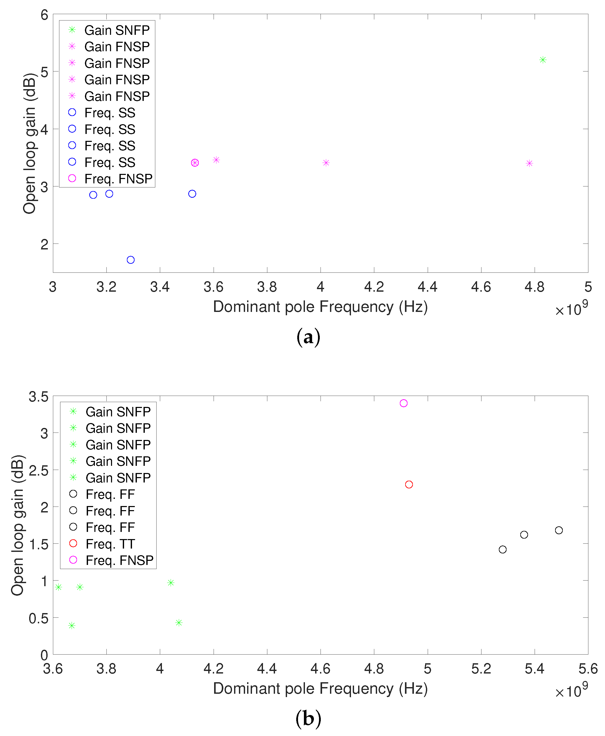
| 2 | TT | (dB) | 2.75 | 3.22 | 3.02 | 2.77 | 3.31 | 3.06 | 2.61 | 3.3 | 3.07 |
| (GHz) | 4.21 | 4.1 | 4.17 | 3.51 | 3.43 | 3.49 | 3.23 | 3.06 | 3.12 | ||
| SS | (dB) | 1.62 | 4.23 | 4.25 | 1.49 | 4.24 | 4.38 | 1.21 | 4.01 | 4.4 | |
| (GHz) | 4.16 | 3.62 | 3.63 | 3.53 | 3.04 | 3.01 | 3.21 | 2.75 | 2.67 | ||
| SNFP | (dB) | 0.42 | 1.67 | 1.68 | 0.16 | 1.57 | 1.57 | −0.16 | 1.43 | 1.49 | |
| (GHz) | 4.51 | 4.16 | 4.17 | 3.86 | 3.5 | 3.5 | 3.53 | 3.15 | 3.13 | ||
| FNSP | (dB) | 4.93 | 4.91 | 4.51 | 5.27 | 5.21 | 4.74 | 5.29 | 5.34 | 4.86 | |
| (GHz) | 3.97 | 3.99 | 4.11 | 3.3 | 3.31 | 3.42 | 2.96 | 2.94 | 3.04 | ||
| FF | (dB) | 2.23 | 2.27 | 2.08 | 2.29 | 2.28 | 2.05 | 2.26 | 2.28 | 2.03 | |
| (GHz) | 4.55 | 4.56 | 4.64 | 3.84 | 3.85 | 3.92 | 3.45 | 3.45 | 3.52 | ||
| 3 | TT | (dB) | 1.57 | 1.7 | 1.52 | 1.63 | 1.69 | 1.45 | 1.64 | 1.7 | 1.43 |
| (GHz) | 4.6 | 4.66 | 4.8 | 3.85 | 3.91 | 4.04 | 3.47 | 3.51 | 3.62 | ||
| SS | (dB) | 1.52 | 2.65 | 2.5 | 1.5 | 2.65 | 2.47 | 1.36 | 2.62 | 2.45 | |
| (GHz) | 4.22 | 4.06 | 4.17 | 3.54 | 3.38 | 3.47 | 3.2 | 3.02 | 3.09 | ||
| SNFP | (dB) | −0.1 | 0.42 | 0.35 | −0.18 | 0.3 | 0.18 | −0.28 | 0.24 | 0.1 | |
| (GHz) | 4.73 | 4.68 | 4.78 | 3.99 | 3.93 | 4.02 | 3.61 | 3.52 | 3.61 | ||
| FNSP | (dB) | 3.19 | 3.07 | 2.77 | 3.39 | 3.18 | 2.82 | 3.49 | 3.26 | 2.87 | |
| (GHz) | 4.45 | 4.58 | 4.76 | 3.72 | 3.84 | 3.99 | 3.33 | 3.44 | 3.58 | ||
| FF | (dB) | 0.89 | 0.87 | 0.72 | 0.91 | 0.81 | 0.61 | 0.93 | 0.82 | 0.59 | |
| (GHz) | 5.11 | 5.22 | 5.37 | 4.32 | 4.43 | 4.55 | 3.9 | 3.99 | 4.11 | ||
| 4 | TT | (dB) | 1.9 | 2.25 | 2.3 | 1.91 | 2.16 | 2.13 | 1.94 | 2.15 | 2.08 |
| (GHz) | 4.77 | 4.81 | 4.93 | 4 | 4.05 | 4.16 | 3.6 | 3.64 | 3.74 | ||
| SS | (dB) | 1.82 | 2.94 | 3.06 | 1.79 | 2.87 | 2.92 | 1.72 | 2.85 | 2.87 | |
| (GHz) | 4.37 | 4.23 | 4.31 | 3.66 | 3.52 | 3.6 | 3.29 | 3.15 | 3.21 | ||
| SNFP | (dB) | 5.2 | 1.15 | 1.27 | 0.43 | 0.97 | 1.02 | 0.39 | 0.91 | 0.91 | |
| (GHz) | 4.83 | 4.79 | 4.88 | 4.07 | 4.04 | 4.12 | 3.67 | 3.62 | 3.7 | ||
| FNSP | (dB) | 3.21 | 3.4 | 3.4 | 3.32 | 3.41 | 3.32 | 3.41 | 3.46 | 3.33 | |
| (GHz) | 4.69 | 4.78 | 4.91 | 3.93 | 4.02 | 4.14 | 3.53 | 3.61 | 3.73 | ||
| FF | (dB) | 1.42 | 1.62 | 1.68 | 1.37 | 1.48 | 1.47 | 1.4 | 1.47 | 1.41 | |
| (GHz) | 5.28 | 5.36 | 5.49 | 4.47 | 4.56 | 4.67 | 4.04 | 4.12 | 4.23 | ||
| 5 | TT | (dB) | 3.89 | 4.17 | 3.82 | 4 | 4.34 | 3.94 | 3.86 | 4.38 | 3.98 |
| (GHz) | 4.02 | 3.96 | 4.07 | 3.38 | 3.3 | 3.39 | 3.06 | 2.94 | 3.02 | ||
| SS | (dB) | 3.05 | 5.53 | 5.3 | 3.04 | 5.71 | 5.57 | 2.77 | 5.55 | 5.67 | |
| (GHz) | 3.89 | 3.44 | 3.49 | 3.29 | 2.85 | 2.87 | 3 | 2.57 | 2.53 | ||
| SNFP | (dB) | 1.39 | 2.5 | 2.38 | 1.19 | 2.45 | 2.33 | 0.88 | 2.34 | 2.28 | |
| (GHz) | 4.34 | 4.05 | 4.09 | 3.7 | 3.4 | 3.43 | 3.38 | 3.05 | 3.06 | ||
| FNSP | (dB) | 6.37 | 6.07 | 5.45 | 6.9 | 6.53 | 5.8 | 6.94 | 6.72 | 5.98 | |
| (GHz) | 3.73 | 3.81 | 3.97 | 3.06 | 3.13 | 3.28 | 2.73 | 2.76 | 2.9 | ||
| FF | (dB) | 3.14 | 3.04 | 2.74 | 3.25 | 3.11 | 2.76 | 3.24 | 3.12 | 2.77 | |
| (GHz) | 4.41 | 4.45 | 4.56 | 3.7 | 3.74 | 3.84 | 3.33 | 3.35 | 3.44 | ||
| Solution | Parameter | Measured Oscillation Frequency and Power Dissipation | ||||||||
|---|---|---|---|---|---|---|---|---|---|---|
| 1 | (V) | −0.53 | −0.55 | −0.6 | −0.65 | −0.7 | −0.75 | −0.8 | −0.85 | −0.9 |
| (GHz) | 4.03 | 4.08 | 4.27 | 4.48 | 4.69 | 4.83 | 5 | 5.15 | 5.32 | |
| (mW) | 30.6 | 31 | 32.1 | 33.1 | 33.9 | 34.6 | 35.3 | 35.8 | 36.3 | |
| 2 | (V) | −0.41 | −0.5 | −0.6 | −0.65 | −0.7 | −0.75 | −0.8 | −0.85 | −0.9 |
| (GHz) | 3.56 | 4.02 | 4.46 | 4.65 | 4.83 | 5 | 5.18 | 5.29 | 5.35 | |
| (mW) | 30.8 | 33.1 | 35.1 | 35.9 | 36.6 | 37.2 | 37.7 | 38.1 | 38.4 | |
| 3 | (V) | −0.27 | −0.3 | −0.4 | −0.5 | −0.56 | −0.6 | −0.7 | −0.8 | −0.9 |
| (GHz) | 2.91 | 3.07 | 3.61 | 4.05 | 4.3 | 4.37 | 4.78 | 5.1 | 5.38 | |
| (mW) | 31.9 | 33 | 35.9 | 38 | 38.9 | 39.4 | 40.3 | 40.9 | 41.2 | |
| 4 | (V) | −0.36 | −0.4 | −0.5 | −0.6 | −0.7 | −0.75 | −0.8 | −0.85 | −0.9 |
| (GHz) | 2.72 | 2.88 | 3.25 | 3.6 | 3.98 | 4.08 | 4.26 | 4.33 | 4.44 | |
| (mW) | 32 | 33.2 | 35.7 | 37.5 | 38.9 | 39.4 | 39.8 | 40.2 | 40.5 | |
| 5 | (V) | −0.41 | −0.5 | −0.6 | −0.65 | −0.7 | −0.75 | −0.8 | −0.85 | −0.9 |
| (GHz) | 3.56 | 3.97 | 4.39 | 4.57 | 4.74 | 4.93 | 5.1 | 5.21 | 5.38 | |
| (mW) | 30.8 | 33.1 | 35.2 | 36 | 36.7 | 37.2 | 37.7 | 38.1 | 38.5 | |
Publisher’s Note: MDPI stays neutral with regard to jurisdictional claims in published maps and institutional affiliations. |
© 2020 by the authors. Licensee MDPI, Basel, Switzerland. This article is an open access article distributed under the terms and conditions of the Creative Commons Attribution (CC BY) license (http://creativecommons.org/licenses/by/4.0/).
Share and Cite
Castañeda-Aviña, P.R.; Tlelo-Cuautle, E.; de la Fraga, L.G. Single-Objective Optimization of a CMOS VCO Considering PVT and Monte Carlo Simulations. Math. Comput. Appl. 2020, 25, 76. https://0-doi-org.brum.beds.ac.uk/10.3390/mca25040076
Castañeda-Aviña PR, Tlelo-Cuautle E, de la Fraga LG. Single-Objective Optimization of a CMOS VCO Considering PVT and Monte Carlo Simulations. Mathematical and Computational Applications. 2020; 25(4):76. https://0-doi-org.brum.beds.ac.uk/10.3390/mca25040076
Chicago/Turabian StyleCastañeda-Aviña, Perla Rubi, Esteban Tlelo-Cuautle, and Luis Gerardo de la Fraga. 2020. "Single-Objective Optimization of a CMOS VCO Considering PVT and Monte Carlo Simulations" Mathematical and Computational Applications 25, no. 4: 76. https://0-doi-org.brum.beds.ac.uk/10.3390/mca25040076