Recent Progress in Photonic Crystal Devices and Their Applications: A Review


1
Department of Physics, Rajdhani College, University of Delhi, M. G. Marg, Raja Garden, New Delhi 110015, India
2
Center for Smart Structures and Materials, Department of Mechanical Engineering, Northwestern University, Evanston, IL 60208, USA
3
Shandong Key Laboratory of Optical Communication Science and Technology, School of Physics Science and Information Technology, Liaocheng University, Liaocheng 252059, China
*
Authors to whom correspondence should be addressed.
Photonics 2023, 10(11), 1199; https://0-doi-org.brum.beds.ac.uk/10.3390/photonics10111199
Submission received: 5 October 2023
/
Revised: 22 October 2023
/
Accepted: 26 October 2023
/
Published: 27 October 2023
(This article belongs to the Special Issue Editorial Board Members’ Collection Series: Photonics Sensors)
Abstract
:The research field of photonic crystals (PhCs) remains active on a global scale. PhCs, which are periodic optical nanostructures with the characteristics of excellent light field confinement and numerous varying degrees of freedom, provide a solid foundation for controlling the movement of light. Periodic variation of the index of refraction in two or three spatial dimensions with a substantial high-to-low ratio generates a number of intriguing phenomena and enables a variety of potential functionalities. Recently, intriguing devices based on PhCs, such as Y-branches, small-diameter bent waveguides, and miniature resonator cavities, have been proposed and extensively utilized. PhC waveguides are considered ideal candidates for a variety of applications, such as in power splitters, logic gates, sensing and communication fields, etc. These exceptional characteristics may facilitate the development of a dense integrated circuit. However, PhC technology is still relatively new and therefore requires additional effort to fully exploit it. This paper reviews the most popular and essential optical components based on PhCs, including power splitters, modulators, polarization maintaining devices, sensors, and lasers, to summarize the most recent developments relating this hot topic. These devices have superior performance and a smaller footprint compared to conventional photonic devices.
1. Introduction
Photonic crystals (PhCs) were discovered in 1987 and were first reported by Yablonovitch [1] and John [2]. Within PhCs, electromagnetic waves scatter. For some wavelengths, destructive interference occurs, resulting in the formation of a photonic bandgap (PBG), which is similar to the energy bandgap of electron waves in a semiconductor. It may be able to influence the propagation of light due to the likelihood of producing a PBG. PhCs are used in a number of notable applications, including self-collimation [3], negative refraction [4], optical diodes [5], and light bending [6].
One-dimensional (1D), two-dimensional (2D), and three-dimensional (3D) photonic crystals represent distinct dimensions of periodic structures designed to control the flow of light. In 1D photonic crystals, refractive index variations occur along a single direction, enabling precise control over light in that dimension. Two-dimensional photonic crystals expand this control to two dimensions, offering more complex light manipulation and enabling the creation of planar structures with applications in waveguides and microcavities. In contrast, 3D photonic crystals extend refractive index variations across all three spatial dimensions, granting comprehensive control over light propagation in volumetric structures. These dimensionality differences lead to variations in band gap properties, complexity of design and fabrication, and suitability for diverse applications, making each type of photonic crystal well-suited for specific optical and photonic device requirements. Although the development of 3D PhCs first attracted a lot of attention, planar 2D PhC devices are now favored because of their comparatively simple production procedure. Many 3D structural traits are present in 2D PhC structures. These factors have sparked an increase in research and development for sub-micrometer and micrometer-sized active and passive photonic elements like logic gates, polarizers, polarization maintaining waveguides (WGs), lasers, and solar absorbers, among others.
PhCs are a good example of a resolution that encourages great performance in sensing applications. PhCs provide strong optical confinement to a very tiny volume, enabling the identification of chemical species classified according to their nanoscale size. The use of PhC WG elements in microfluidic [7] and biochemical sensing [8] has lately come under investigation. In sensing applications, a number of photonic structure designs based on various platforms have been extensively researched and used [9,10,11].
A 1D PhC consists of a periodic variation of the refractive index in the direction of light propagation. However, it provides a homogeneous medium in the other two directions [12]. The refractive index varies in two directions for 2D PhCs, but not in the third direction. This can be realized just by introducing a hole in a high-refractive-index material, e.g., silicon [13]. Three-dimensional PhCs can be fabricated by varying the refractive index of the material in all three directions, such as the stack of spheres made of some dielectric material kept in air [14]. The propagation of light in a periodic structure can be studied by the periodic arrangement of atoms, such as the propagation of electrons. PhCs are frequently mentioned in theories like energy bands, the Bloch theorem, and Brillouin zones. One-dimensional PhCs, also known as multilayers, lack a complete PBG, while 3D PhC fabrication is difficult because of their narrow lattice constant. However, 2D PhCs comprise a full PBG and a simpler fabrication step compared to 3D PhCs, making them more appealing to researchers. A 2D PhC is composed of an air pore arranged in a dielectric substrate or a cylindrical rod made of dielectric material submerged in air. The PBG of a PhC can be tuned by altering the radius of the rod, the lattice constant, and the refractive index of the dielectric. The resonant cavities are considered one of the potential candidates in order to create a tunable optical filter for dense wavelength–division multiplexing (DWDM) systems [15,16,17]. For DWDM systems, the resonant cavities with a high quality factor (Q-factor) filter the desired wavelengths with a suitable bandwidth. The adjustable filters can also be formed by introducing composition improvements to these cavities. In 2010, Rostami et al. utilized this technique to develop a demultiplexer [18]. The advantages of PhC cavities for optical interconnects can be summed up in one number: the resonator’s interference order. The free spectral range (FSR), and thus the capacitance, increase by reducing this number. The conceptual limit of this theory is a PhC resonator, which often serves as the fundamental cavity mode. Due to their wide FSR, single-mode (SM) PhC cavities with various cavity resonances can be constructed in large arrays. When the PhC interacts with the incoming light, it gets reflected from each interface. A high reflection is witnessed for the particular wavelength of light when this condition is fulfilled.
Two dimensional PhCs, which are periodic in two directions and have a photonic band gap for light propagating in the plane of periodicity, are extensively used in a diverse range of applications, such as high Q-cavity devices for efficient light confinement [19], slow light optical waveguide devices [20], and optical waveguides with sharp bands and low losses for photonic integration [21]. Photonic crystal waveguides (PCWs), a class of 2-D PhC-based devices, offer an intriguing framework for making use of slow light effects. The large group index, which is a result of in-plane back-and-forth scattering at optical frequencies at the boundaries of photonic transmission bands, is where the slow light effects in PCWs arise [22].
This review is organized in the following manner: Section 2 contains basic ideas of the PhC structure; Section 3 describes the PhC-based polarization maintaining WGs; Section 4 covers the literature showing the role of PhC in the development of solar cells; Section 5 covers the potential of PhC in sensing; Section 6 discusses the PhC-based logic gates; and Section 7 presents an overview of the PhC-based amplifiers. Section 8 discusses the future prospects and challenges related to PhC-based devices, and finally, an overall conclusion is drawn in Section 9.
2. Photonic Crystal Structures
In the past decade, a strong effort has been made to control and manipulate light propagation. The propagation of light in a periodic material has been a burning topic of research for a large span of time. John [1] and Yablonovitch [2] separately reported the concept of PhC in 1987, utilizing the concept of semiconductor crystals along with the analogy of an electronic band gap. In general, PhCs can be defined as a periodic dielectric material with periodicity in one, two, or all three orthogonal directions; therefore, they are known as 1D PhCs, 2D PhCs, and 3D PhCs. Among these three structures, a 2D PhC combines most of the interesting optical characteristics with the availability and accessibility of fabrication, and thus has wider research applications. It took a century to discover 2D photonic band gap (PBG) materials after the identification of 1D band gaps. The 2D system shows most of the significant properties of PhCs, ranging from nontrivial Brillouin zones to topological sensitivity, even with a minimal index contrast. They hold great potential for validating the most widely favored PhC devices. Understanding 2D PhCs hinges on recognizing that the fields in two dimensions can be divided into two polarizations by virtue of their symmetry: transverse electric (TE) and transverse magnetic (TM). In the TE state, the electric field resides within the plane, while the magnetic field extends perpendicularly to it. Conversely, in the TM state, the magnetic field lies within the (xy) plane, while the electric field is perpendicular (z). Within 2D PhCs, a diverse array of configurations is possible, thanks to variations in permittivity along two directions, with the medium remaining uniform in the third direction. Utilizing PhCs with 2D periodic lattices significantly broadens the scope for engineering photonic band structures. Two-dimensional PhCs offer a broad range of configurations due to the periodic variation of dielectric materials along two directions, while the third direction remains uniform. Two-dimensional PhCs can be categorized into two types: (i) the air holes in materials of a high refractive index and (ii) the rods of materials of a high refractive index. The former type of 2D PhC can be easily fabricated just by etching holes periodically in high-dielectric materials such as gallium arsenide (GaAs), silicon (Si), germanium (Ge), etc. [3]. Because of the periodic variation of the refractive index, the PhC possesses a PBG, which is defined as a range of frequencies that is prohibited from propagating inside the crystal. This particular unique feature has been exploited widely in order to form waveguides by introducing line defects in the PhC structure. The line defect in PhC introduces a guided mode in PBG, and it can therefore be utilized to guide light from one point to another. The allowed frequencies in the PBG are guided via defect and out-of-plane confinement based on the total internal reflection (TIR) phenomenon. PhC WGs fabricated by removing holes from a PhC structure are shown in Figure 1a. The dispersion relation diagram of the PhC WG (considering 400 nm diameter holes arranged periodically in a hexagonal manner with a lattice constant of 500 nm) is calculated using the plane wave expansion method and is shown in Figure 1b. The grey-shaded region in Figure 1b represents the leaky zone, while the black lines exhibit the guided modes [4].
A silicon-on-insulator (SOI) is generally preferred for fabricating PhC WGs due to its favorable optical characteristic, which appears at 1.55 μm and complementary metal–oxide semiconductor (CMOS) fabrication compatibility for cost-effective and high-volume production. An SOI comprises a thin silicon guiding layer with a refractive index (RI) of 3.45 on a thick buried oxide cladding layer with an RI of 1.45, which provides a strong confinement of the light. The high RI of the silicon guiding layer makes the SOI an excellent choice to fabricate the PhC structure with a higher PBG, which is often required in various applications. The thickness of the guiding layer plays a crucial role in determining the properties of the PhC slab. If the guiding layer is too thin, then the PhC slab will provide weak confinement, as the guided mode will be very close to the light cone. On the other hand, the thick slab generates higher-order modes, which may destroy the PBG. The optimum thickness of the PhC slab satisfying the single-mode condition can be defined as follows [4]:
where λ0, n, n1, and n2 represent the free-space wavelength, RI of the guiding layer, and upper cladding and lower cladding, respectively. According to the above Equation (1), the maximum optimized thickness of the guiding layer for a PhC on an SOI is hmax = 273 nm, operating at a wavelength of 1550 nm. Therefore, the guiding layer thickness must be smaller than 273 nm to satisfy the single-mode condition, which will increase the transmission.
The 2D photonic crystal slab plays a crucial role among label-free optical biosensing methods. The 2D photonic crystal slab biosensing holds significant promise for the miniaturization, integration, and simultaneous detection of multiple targets when integrated with microfluidic chips. Furthermore, the slow light effect inherent in 2D PhC slabs improves light–matter interactions, while ultra-high quality (Q) factor cavities, proportional to the cavity volume (V), enable the continuous reduction in detection limits through innovative design. These characteristics collectively render the 2D PhC slab a favorable option for the fabrication of optical biosensor transducers. The 2D PhC slab biosensor generally utilizes the evanescent field, which is confined within the waveguide, in order to detect the molecular interactions. This evanescent field behaves as an electromagnetic field that appears along the surface of the waveguide during total internal reflection. It has the ability to interact with nearby materials, forming an external region sensitive to changes in the refractive index. When the measurand attaches to receptors on the waveguide’s surface, the accumulation of molecules with varying refractive indexes changes the external refractive index, perturbs the evanescent field, and subsequently influences the behavior of the propagated guided light within the waveguide. The sensitivity of the devices is formally quantified as the ratio of the minimum shift in the resonance wavelength to the alteration in the refractive index, i.e., S = Δλ/Δn.
Creating a 2D PhC biosensor typically involves a two-step process. First, one must devise an appropriate lattice structure to establish the frequency position of the band gap and the desired mode type. The prevailing approach for this is the plane wave expansion (PWE) method. Second, the sensor’s design needs to incorporate a practical sensing component, which often entails the introduction of one or several defect states to capture alterations in the spectrum caused by changes in the refractive index of the slab surface due to biomolecule interactions. The finite-difference time-domain (FDTD) method is the most commonly employed technique for this purpose.
3. PhC-Based Polarization Maintaining WGs
The polarization dependency of PhC structures is one of its distinguishing properties, which has been used to develop numerous polarization-maintaining devices such as polarizers. Polarizers are very helpful in optical systems because they filter out undesirable polarized light for specialized applications. The polarizer’s operation is based on the polarization-dependent propagation of a PhC waveguide (WG), which differs from standard polarizers. It is founded on the specific features of two-dimensional (2D) PBG materials. Unpolarized light may be split into two components: transverse electric (TE), which have an E-field parallel to the periodic plane; and transverse magnetic (TM), which have a magnetic field parallel to the periodic plane. In 2D PBG materials, TE and TM polarized light propagations can occur independently of one another. It is important to note that the band structures and PBGs of the TE and TM polarizations are distinct. Both passive and active PBGs are possible. The Maxwell equations may be used to completely explain how passive or active PBGs interact with light. Similar to how Bragg reflection and diffraction gratings interact with and confine light, PBGs use multiple scattering and diffraction to do the same. The local EM field may be significantly impacted by PBG defects. Consequently, it has been demonstrated that these PBGs possess peculiar optical resonances, and their characteristics may be customized by picking the suitable bandgap and generating defects. The TE and TM polarizations propagate independently of one another in 2D PBG materials. In other words, the PBGs and band structures for the TE and TM polarizations are distinct. Figure 2 depicts typical band structures of a 2D PBG crystal projected in the direction of incoming light, from which some general characteristics of EM wave propagation may be suggested. The frequency of an EM wave and the band structure of the PBG crystal both affect its transmission. Both TE and TM waves can transmit in areas where the TE and TM bands overlap. Both TE and TM wave propagations are prohibited in the area where TE and TM PBGs intersect. The propagations of the TE and TM polarizations in 2D PBGs are independent of each other, or we can say that the TE and TM polarizations have their own band structures and PBGs [23].
Chun et al. proposed a PhC waveguide-based polarization-sensitive polarizer. Here, a 2D PBG crystal consisting of dielectric rods arranged in a square lattice form is designed and used to make a polarizer. A polarizer with a 40 μm long 1D PhC waveguide with a 40 dB extinction ratio has been reported by Zhao et al. [24]. Similarly, polarizers with improved extinction ratios have been designed using the 1D PhC waveguide structure [25,26,27]. Apart from this, a transverse magnetic (TM) polarizer based on the 1D PhC structure has been proposed with a high extinction ratio of 8.5 dB/μm by Kim et al. [28]. Recently, Pandey et al. presented a brief report on the tunable dispersion characteristics of TE and TM modes in a ternary polymer PhC composed of graphene, silicon, and polymer as nanolayers. By employing a TMM, it has been investigated that the structure shows novel ideas of tunability with variations in the incident angle and polymer thickness in which the Bloch waves are affected [29]. The performance of some photonic devices using TM-polarized light is astounding [30]. Additionally, TM-polarized light is useful for sensing applications because, in contrast to TE-polarized light, its evanescent field penetrates farther into the top and bottom cladding.
Additionally, TM-polarized light is used in polarization multiplexing devices to enable the majority of the channel capacity. As a result, it is recommended that TM-polarization pass devices are essential for effectively developing photonic-integrated circuits. In order to profit from the large index contrast of silicon-to-silicon dioxide, strong structural birefringence, considerable optical nonlinearities, and well-established CMOS manufacturing capabilities, a bulk of integrated circuits is being constructed on an SOI platform [31].
Recently, Jerakani et al. proposed an ultra-compact polarizer by using the linear birefringence effect of the uniaxial anisotropic material. They proposed a 1D PhC structure having an anisotropic defect layer, which is used to break the degeneracy of the TE and TM modes of resonance [32]. Figure 3 shows the 1D PhC structure used for the polarizer which has alternating YVO4 and SiO2 layers. The TE and TM band diagrams of the proposed structure are shown in Figure 4, respectively.
There are several polarization devices presented by the researcher that are based on photonic crystals [33,34,35,36,37,38,39,40]. In [41], Kang et al. show that by tuning the relative phase of multiple inputs for coherent control, it is possible to attain coherent complete polarization conversion. They experimentally demonstrated flexible polarization control in the terahertz region using a silicon photonic crystal slab. The schematic diagram of the photonic crystal slab is shown in Figure 5.
Also, Xintao shows 2D valley photonic crystals with dual-polarization by simultaneously opening two frequency degenerate Dirac cones. The opposite-valley Chern numbers of the two band gaps with distinct polarizations are supported by opposite-phase vortex distributions of the bulk modes and the opposing Berry curvatures. Due to this circumstance, the bulk and edge modes, which are located in opposing valleys, exhibit polarization-dependent refraction. In this instance, they also illustrated topological valley transfer that is polarization-independent [42].
The fundamental parts of integrated photonics and communication systems include polarization beam splitters (PBSs) [43,44] and optical power beam splitters (BSs) [45]. While a PBS offers a distinct routing of light in the two polarization states known as the TE and TM [46,47], a BS separates the entering light into many pieces at the output [48,49]. Two-dimensional PhCs can be used as polarizing beam splitters, another important device necessary for electromagnetic wave polarization control, because their band gap profiles are polarization-dependent. Such devices were created for a number of reasons, one of which is that, unlike traditional polarizing beam splitters, they do not separate polarizations using Brewster’s angle. Since retroreflection is a possibility, the angle between the wave vectors of the transmitted and reflected beams can theoretically range from 0° to 180°. Beams produced by a high-quality polarization splitter must be almost entirely polarized. This means that the TM and TE band gaps must be separated in order for a 2D photonic crystal to act as a polarizer. In this scenario, the photonic crystal can function as a polarizer in the area of the spectrum where the waves of one polarization are totally transmitted, but the waves of the other polarization are virtually entirely reflected. Although the band gap profiles for various polarizations often do not match completely for a 2D photonic crystal due to the factors previously addressed, they may not be sufficiently separated to create highly polarized beams. Because of this, some crystals might not possess the required efficiency and/or practical bandwidth to be employed as polarizing beam splitters. Because of their diminutive size, PBSs built on PhCs are very appealing [50,51]. Light passing through a PhC could come into contact with a refractive index that is negative or positive. The three factors of refractive index contrast, angle of incidence, and slab thickness interact to produce the two refraction situations. By effectively utilizing these qualities, simple and effective optical modules to steer the light are likely to be realized. As an illustration, a passive optical device that acts as a PBS is shown, with the polarization of the TM and TE waves twisted in the opposite positive and negative directions.
In 2003, Solli et al. experimentally demonstrated PhC-based polarizers and polarizing beam splitters. They used a hexagonal-type PhC structure and obtained the transmission and reflection characteristics of the proposed beam splitter [52]. The polarization extinction ratio (PER), a crucial indicator of merit, is used to gauge PBS efficiency. In 2021, Butt et al. proposed and examined a 2D PhC heterostructure compact design for a PBS and light steering applications. Given their small size and great attractiveness, the PER that the design provides is >30 dB [53,54]. There are several unique designs of PhC-based beam splitters that have been proposed and studied extensively [55,56,57,58].
Recently, by using a 2D heterostructured PhC, a small PBS device has been quantitatively studied. The PhC formations are made using a special method that allows PhC-1 to transport light with self-collimated TE- and TM-polarization. The design of PhC-2 creates a PBG for TE-polarized light. However, an interference-free transmission of TM-polarized light is possible. When these two unique PhC formations are merged at an angle of 45°, the self-collimated TE-polarized light interferes with the PC-2 and is reflected at a steep 90° bend, while the self-collimated TM-polarized light may flow through both forms since it does not encounter any PBG on its path. Therefore, in a small space, both polarizations are separated at a 90° angle [59]. The two optimum PC forms should be merged for the polarization division-multiplexing system so that the light with the TE and TM polarizations can divide at 90 degrees. The construction of a PBS, which may be used as an on-chip PDM system, results from the unique union of PC-1 and PC-2. As seen in Figure 6, both structures are united at a 45-degree angle. The normalized electric field mapping of TE-, TM-, and TE + TM-polarized light at 1500 nm is shown in Figure 7.
4. PhC-Based Solar Cells
The recent year witnessed a wide exploitation of PhCs in solar cells due to their unique optical properties, i.e., PBG and slow photon effect. The introduction of PhCs can successfully modulate the distribution and propagation of photons in solar cells. Therefore, the key to improving the efficiency of photoelectric conversion can only happen through a full understanding of the optical characteristics of PhCs. At present, PhC structures are being utilized in quantum-dot-sensitized solar cells (QDSSCs) and dye-sensitized solar cells (DSSCs), but comparatively few in the field of perovskite solar cells (PSCs) [60]. This section summarizes the applications of various types of PhCs in sensitized solar cells and silicon solar cells, and their possible limitations and advantages are analyzed.
One of the most promising ways to improve the performance of a thin film solar cell is to improve light trapping [61]. Light trapping in the thin film is usually improved via a surfaced metal back reflector that allows for the dispersion of light inside the absorber layer and therefore significantly increases the optical path length of the photons, which improves the light trapping inside the thin solar cells. PhCs can be integrated along with a suitable absorber, which helps in selective solar absorption. By varying the structural parameters and moving the PBG, the absorption cut-off can be tuned. Additionally, PhCs can significantly boost absorption by tuning the quality factor [62]. In 2019, Cen et al. reported a numerical analysis and exhibited a perfect absorption of monolayer graphene, showing a high quality factor and high sensitivity [63]. The author studied the single-band absorption of graphene via impedance-matching and the critical coupling effect. The analysis exhibited a high Q-factor of 664.2, achieved by varying the ratio between the structural period and the radii of the elliptic cylinder air hole. A PhC offers the benefit of incorporating diffraction, where the photon momentum (k) can be dispersed away from the specular path with k = ki + g, where g is a reciprocal lattice vector and ki is the incident wave vector.
In 2012, Mavrokefalos et al. reported on the light absorption within the crystalline silicon, which was significantly improved by inverting the nanopyramid light-trapping technique for crystalline silicon thin films, as shown in Figure 8a [64]. In this reported work, the author proposed an inverted nanopyramid light-trapping technique for crystalline silicon thin films, fabricated at a wafer scale using a cost-effective, wet, etching procedure that significantly enhances the absorption of light within the crystalline silicon thin films. Furthermore, the author also validated that the absorptivity of crystalline silicon thin films with a thicknesses less than 10 μm is significantly comparable to that of planar crystalline silicon wafers with a thicknesses greater than 300 μm, as shown in Figure 8b. From the investigation, it was observed that these structures can not only significantly minimize the processing costs, but also provide the improved efficiency required to enable viable crystalline silicon thin film solar cells in the future.
In 2014, Yu et al. reported semitransparent polymer solar cells (STPSCs) utilizing a PhC reflector to achieve 5% conversion efficiency [65]. The 1D PhC comprises multiple optimized layer WO3/LiF pairs, as shown in Figure 9. This optimized 1D PhC reflected light back into the STPSCs because of the PBG. The STPSCs with eight pairs of 1D PhCs exhibited an attractive performance, along with a short-circuit current density (Jsc) and power conversion efficiency (PCE) of 9.76 mA/cm2 and 5.16%, respectively. A maximum enhancement of 20.2% in Jsc was achieved, while the PCE was obtained to be increased by ~21.7%.
In 2015, Sergey et al. reported a numerical solution of Maxwell’s equations, near-perfect solar light trapping and absorption over the 300–1100 nm wavelength band in PhC architectures, amenable to fabrication using the wet-etching technique, and requiring less than 10 μm of crystalline silicon. The PhC comprises a square lattice of inverted pyramids with sides consisting of several (111) silicon facets, and the pyramid center-to-center spacing was used, varying from 1.3 to 2.5 μm. On the wet-etched slab with a height of 10 μm and a lattice constant of 2.5 μm, the author observed a maximum photo current density of 42.5 mA/cm2, falling not far from 43.5 mA/cm2, corresponding to 100% solar absorption. The author also investigated that these wet-etched structures required double the volume of silicon compared to the overall numerically optimum PhC structure. In the same year of 2015, Zhang et al. introduced TiO2/SiO2 1D PhCs as active layers into photonic solar cells [66]. To maintain a high reflectivity, the TiO2 and SiO2 microstructure layers were optimized in order to reduce the thickness of the photonic crystal layer. On the other hand, the author utilized the photonic crystal structure color to visualize and realize multicolor, non-transparent photonic solar cells with blue, blue–green, and green hues. At the same instance, the PhC reduces thermal gain and improves the reflectance of the incident light at a specific frequency, which is highly beneficial for the enhancement of the conversion efficiency for practical applications. In 2016, Ramos et al. utilized angular physical deposition to accurately control the growth of nanorods [67]. They reported the preparation of three types of 1D PhCs that can be used as photonic solar cell photoanodes by controlling the angle of physical deposition. With the reported design, the author achieved conversion efficiencies of 6.39%, 10.94%, and 12.03%, respectively.
In 2017, polymer solar cells were reported as an important category of the next generation of new thin-film solar cells. This technology has gained huge attention in recent years, as its energy conversion efficiency was reported to be more than 13% [68]. Following the results, Shi et al. reported a 1D PhC with various Bragg reflection wavelengths and implemented it in translucent polymer solar cells [69]. The bulk heterojunction active layer of the translucent polymer solar cell was 90 nm thick (PTB7-Th: PC71BM). Considering the advantages of this high-performance thin film device structure, the author fabricated semitransparent photonic solar cells by introducing an ultra-thin transparent silver cathode by replacing a thick silver mirror cathode, resulting in high-performance, semitransparent, photonic solar cells with a conversion energy of over 6% and an average visible transmittance between 20% and 30%. In the same year of 2017, Gupta and Janyani improved the performance by using a 2D PhC-based thin layer heterojunction gallium arsenide (GaAs) solar cell with a periodic pattern [70]. In their reported work, the authors compared two structures: (i) having a PhC structure extended from the top transparent, conducting oxide to the p-AlGaAs window layer placed above the GaAs material; and (ii) the PhC structure etched only in a transparent conducting oxide. A comparative analysis of the structure with the planer cell and Lambertian light trapping limits was also performed, and a significant increment in the efficiency was observed for thinner active layers, showing the advantage of a wavelength scale. The ‘Lambertian’ term refers to a type of surface or material that exhibits diffuse reflection, meaning it scatters incident light in all directions uniformly. In the context of solar cells, ‘Lambertian’ surfaces are often used to enhance light trapping and absorption within the cell structure. The results exhibited that the PhC structure (etched inside p-AlGaAs)-based solar cell exceeded the efficiency of the double-antireflection coating (ARC)-based structure by more than 18% for a 50 nm thin active layer cell. Later, in 2018, Zhang et al. proposed a numerical analysis of a multi-junction solar cell structure [71]. The designed structure was a combination of grating and a 1D PhC considered to be made of crystalline silicon and silicon dioxide. It uses gratings to increase its effective optical path. The design was optimized carefully, leading to remarkable efficiency for the cells with very thin silicon active layers due to the significantly enhanced absorption. In 2019, Bhattacharya et al. achieved 29% power conversion efficiencies by utilizing thin, crystalline silicon, following the efficacy of wave-interference-based light trapping and carrier transport in a parabolic−pore PhC [72]. In the reported work, the author demonstrated the geometry of a simple PhC solar cell which enables the power conversion efficiency of a single-junction c-Si solar cell to exceed the previously reported theoretical limits.
In the most recent article published in 2022, Morsy and Saleh reported another PhC solar cell utilizing GaAs to develop nano-solar cells [73]. A nano-solar cell based on a 2D PhC ARC trapping layer and a 2D-graded-index GaAs active layer was reported and numerically investigated using the finite-difference time domain (FDTD). The proposed cell absorption and conversion efficiency were analyzed as a function of the cell layer thickness in comparison with the Lambertian absorption and cell efficiency limits. All the simulations were performed in the range of 300 to 1100 nm using the FDTD technique, where the 2D PhC structure was shown by indium tin oxide nanorods in an air background. The study exhibited that the design of a 100 μm2 nano-solar cell achieved a 39.2% conversion efficiency. In addition to these structures, several other structures were also reported in the past decades, which are summarized in Table 1.
From the above discussion, we can clearly see improvement in the performance of various types of PhC solar cells. However, can also be observed that the technology still faces a huge research gap due to the limited exploitation of the features of PhCs. To overcome various challenges, researchers should fully understand the PhC light control performance, the selection of the appropriate PhC structure, and the illumination direction. At present, photonic crystal structures are widely used in dye-sensitive solar cells and quantum-dot-sensitive solar cells, but relatively few in the field of perovskite solar cells. It is worth noting that although PhCs have several excellent optical control properties, it is difficult to achieve the thickness requirements of a perovskite solar cell because of the limitations of the preparation technology and structure of PhCs.
5. Photonic-Crystal-Based Sensors
Because of the growing demand for sensing devices, PhCs emerge as a potential tool in healthcare [93,94], physical parameter monitoring [95,96], defense [97], food quality control [98], and aerospace [99]. The surface of PhCs is made of a periodically modulated dielectric material that can be modified in order to create a PBG, which helps prevent light from propagating at particular wavelengths [100]. Consequently, the local optical modes of a PhC can be utilized as a label-free and highly sensitive platform for monitoring chemical and physical changes in the surrounding environment. In order to evaluate the sensing performance of such devices, several parameters were investigated such as sensitivity, response time, selectivity, stability, and the limit of detection (LoD) [101].
In their initial days, PhCs were popular among gas-sensing applications, as they required light to be modulated through the waveguide and recorded on the detector. PhCs based gas sensors were considered the safest way to detect hazardous gas without compromising sensitivity and selectivity compared to electrochemical, chemiresistive, and ratiometric sensors. Gas sensors based on PhCs are reported for the mid-infrared range for various toxic gases; for example, CH4, CO2, and CO exhibited absorption lines in the mid-IR wavelength region. A high-precision gas index sensor based on a PhC air–slot cavity was proposed, offering a sensitivity of 510 nm/RIU [102]. In 2012, Jun reported that a surface plasmon resonance (SPR) nanocavity antenna array for gas sensing application achieved a maximum sensitivity of 3200 nm/RIU [103]. A guided-mode resonance gas sensor with a sensitivity of 748 nm/RIU was reported [104]. In addition to gas sensing applications, PhCs also gained huge popularity in chemical- and biological-sensing applications. From a technical point of view, the optical sensors based on PhCs, including PhC optical fiber, also known as PCF, and integrated planar PhCs, are suitable for label-free detection and multiplexing. For example, in 2012, Zou et al. reported large-scale chip-integrated PhC sensor microarrays, and demonstrated their application in biosensing on an SOI-based platform [105]. These days, integrated PhC-based optical sensors are considered the most popular class of photonic sensors, which are generally utilized to monitor physical and chemical parameters. In 2013, Lu et al. also fabricated an integrated temperature sensor based on an enhanced pyroelectric PhC [106]. The sensing response of the devices was achieved with the pyroelectric effect of lithium–niobate, in which a suitable air–membrane PhC cavity has been fabricated. The wavelength position of the cavity mode is tuned at 11.5 nm for a temperature variation of only 32 °C. The reported device exhibited an average temperature sensitivity of 0.359 nm/°C for an active length of around ~5.2 μm. The main advantages of these sensing configurations are their high light confinement, excellent sensitivity, and selectivity in the sensing mechanism.
In 2014, Shafiee et al. utilized nanostructured PhCs for the label-free detection and quantification of intact viruses (HIV-1) from biologically relevant samples [107]. Figure 10 illustrates the schematic of a nanostructured PhC HIV sensor platform. In the proposed scheme, the PhCs resonantly reflect a very narrow wavelength band during illumination with a broadband light source. The surface of PhC-adsorbed biotarge induces a shift in the resonance spectral peak, which is detectable with a <10 pm wavelength resolution. The process allows for the successful detection of a small number of viruses that sparsely populate the transducer surface. In the reported work, the authors successfully detected HIV-1 in serum and phosphate-buffered saline (PBS) samples with viral loads varying from 104 to 108 copies/mL.
In 2015, Bouzidi et al. reported a tiny and portable gas-sensing system using 1D PhCs [108]. The sensor comprises a 1D PhC formed using alternate layers of magnesium fluoride (MgF2) and silicon (Si), with a vacant layer in the middle. The empty layer was later filled with the polluted air, which had a refractive index closest to that of pure air, varying from 1.00 to 1.01. Transmission spectra were used here for the real-time detection of gaseous environments. The peak frequency of the transmission spectra was observed to be sensitive to the air–gas mixture with a high sensitivity of 700 nm/RIU. In 2016, Farhat et al. reported a surface-plasmon-resonance-based liquid crystal photonic crystal fiber (PCF) sensor for a temperature sensor [109]. The reported work briefly exploits the coupling characteristics between the fundamental mode inside the designed PCF infiltrated with a nematic liquid core and the plasmonic mode on the surface of a nanogold wire. The designed sensor exhibited a high sensitivity of 10 nm/°C for temperatures ranging from 30 to 50 °C. In 2017, Liu et al. reported an refractive index sensor using high quality factor bound states in free-space-coupled PhC slabs [110]. Figure 11 illustrates the schematic diagram and key parameters of the proposed design, with angle and polarization defined for the incident light beam. The reported paper demonstrates a numerical investigation over single and coupled bi-layer PhC slabs that possess a simultaneously high S and Q near the bound states in the continuum. The reported article validated the performance of the device experimentally and numerically. The numerical analysis exhibited S > 800 nm/RIU and Q > 107 for refractive index sensing in the 1400–1600 nm optical wavelength band, while experimentally, the value achieved 94 nm/RIU and 1.2 × 10⁴ for S and Q, respectively.
In 2018, Maurya et al. proposed a 2D layered nanomaterial (graphene, MoSe2, MoS2, WSe2 and WS2)-decorated 1D PhC refractive index sensor based on the Kretschmann configuration [111]. The 2D nanomaterial shows an excellent sensing response due to its superior adsorption, as well as absorption properties. The reported design comprises alternate layers of 2D nanomaterials and silicon, as shown in Figure 12. The performance of the design, including sensitivity, quality factor, resolution, and evanescent field penetration depth, was investigated and compared with a 1D PhC decorated with polymethyl methacrylate (PMMA) in place of silicon. An increased shift in resonance angle was obtained along with a high quality factor by replacing PMMA with silicon, but at the cost of poor resolution.
In 2019, Snapp et al. reported a colloidal PhC strain sensor integrated with a graphene phototransducer [112]. In the reported work, the author used a colloidal solution to develop a PhC which changes color in the presence of externally applied strain. This hybrid sensing system allows for a direct visual perception of strain, while strain quantification via electrical measurement of the hybrid system outperforms that of crumpled graphene strain sensors by more than 100 times. In 2020, Resende et al. developed a PhC sensor for the label-free and target-specific detection of urinary venous thromboembolism biomarkers using molecularly imprinted polymers [113]. The molecularly imprinted photonic polymer (MIPP) was achieved by manipulating an imprinted polymer on highly ordered silica nanoparticles assembled via vertical deposition. Owing to the hierarchical sensing configuration, the resulting MIPP exhibited optical properties that changed upon rebinding of the target analyte. The sensor exhibited a linear response, varying from 0.2 ng mL−1 to 22 ng mL−1, and showed a lower limit of detection of 0.13 ng mL−1. In the most recent article published in 2022, Kawasaki et al. reported the application of PhCs for monitoring SARS-CoV-2 in saliva to tackle the global pandemic [114]. The sensor comprises an imprinted photonic crystal thin film functionalized with an anti-SARS-CoV-2 spike protein antibody, enabling label-free, highly sensitive, and selective detection using a smartphone-equipped optical setup. The sensing response of the sensor was examined with artificial saliva, and a specific and quantitative detection of the spike protein was successfully obtained, with a low LOD of 429 fg/mL. Additionally, the author also provides an IoT-based, user-friendly interface to store the result data and return it immediately to the patient. The schematic of the reported sensors is shown in Figure 13.
Sensor applications based on PhC also hold significant promise in the realm of liquid-based sensing. In 2011, Pu et al. reported such a study and explored the influence of temperature on the band gap properties of magnetic fluid-based PhCs [115]. In the reported article, a method was developed to extract temperature-dependent structural information from existing data, yielding crucial parameters for band diagram calculations. The research reveals that temperature has a limited impact on the mid-frequencies and positions of forbidden bands, but it can alter the number of forbidden bands at specific magnetic field strengths. Later, in 2016, Su et al. numerically designed a novel PhC magnetic field sensor, featuring a shoulder-coupled resonant cavity filled with magnetic fluid [116]. By tracking the changes in the resonant wavelength, the sensor achieves magnetic field sensing, with greater sensitivity and improved performance obtained through specific infiltration schemes, resulting in an optimal structure with eight air holes filled with magnetic fluid. PhCs’ inherent ability to seamlessly interact with liquids opens doors to several practical applications. Such devices can be employed to monitor and analyze a broad range of materials in liquid form, from biological molecules and pathogens to environmental contaminants. This versatility positions PhC-based sensors as powerful tools for advancing fields like medical diagnostics, environmental monitoring, and food safety, where precision and sensitivity are paramount. The ease with which photonic crystals can be infiltrated with liquids underscores their potential to revolutionize liquid-based sensing, offering a path to more effective and efficient detection and analysis methods. In addition to several advantages, such as its small size, immunity to electromagnetic interference, high sensitivity, strong light confinement, etc., it also possesses a limitation in terms of its fabrication and implementation. The sensing material is disadvantaged by poor adhesion during its deposition on a PhC [97]. In some cases, the author fabricated the Panda fiber by integrating the sensing material into the silica cladding and monitoring the birefringence to detect hydrogen leakage [117]. Overall, the sensing devices based on PhC offer a huge possibility, ranging from biomolecules to gas detection, and can hence be considered a potential candidate for the next generation of sensing. In addition to the PhC sensors we reviewed above, there are some other sensors that have been reported in the past decades, which are summarized in Table 2.
6. PhC-Based Logic Gates
All-optical systems have garnered significant interest among researchers in recent years due to their exceptional applications in fiber optic communication, optical computing, and optical signal processing [150]. For the realization of all-optical devices, PhCs are offered a new avenue [151,152,153]. These devices utilize the periodic arrangement of crystals with varying refractive indexes to regulate the passage of light. PhCs have great qualities such as strong light confinement, compact size and high-speed light propagation, quick response time, wide bandwidth, and low-power dissipation [150]. Light confinement is strong in silicon PhC waveguides, making them appropriate for the design of combinational and logical optical circuits. The periodic arrangement of atoms in a crystal gives rise to energy bandgaps in PhCs. Another intriguing phenomenon that can be produced with PhCs is the prevention of light transmission via optical switching techniques [154]. In this way, researchers [155] have proposed a half-subtractor using PhCs as a possible structure for usage in arithmetic logic circuits. To calculate addresses and increment or decrement operators, a half-subtractor plays a crucial role. The most fundamental combinational logic circuit utilized in digital electronics is the half-subtractor. This circuit allows for the subtraction of two binary digits and creates two output bits (difference and borrow). Similarly, Rao et al. [156] have designed the all-optical MUX using square lattice-type silicon rods and a combination of T- and Y-shaped waveguides. Here, silicon rods have been used for back reflection that also reduces the power loss. This structure consists of a silicon rod with a diameter of 0.2a, a refractive index (RI) of 3.4, and a lattice constant of 0.6 µm. Using silicon junction rods with radii of r3 = 0.3a and r4 = 0.25a at junctions J1 and J2, respectively, prevents undesirable back reflections at the input ports. A PC-based all-optical MUX is shown in Figure 14. The design is composed of two T-junctions and one Y-junction, together with three horizontal and two vertical waveguides. Two horizontal waveguides on the right side of the device are utilized as the reference (R) and select (S) input ports, while another horizontal waveguide on the left side serves as output port Y. A waveguide on the top is utilized for input port A, while a waveguide on the bottom is used for input port B. The suggested all-optical device is based on the phenomenon of beam interference, as shown in Figure 15. The theory of wave optics states that interference occurs within waveguides. Depending on the beginning phase and path covered by incoming light signals, a constructive or destructive interference would ensue.
Rao et al. [153] also proposed a reversible logic gate for a lossless digital system. It is very impressive because it lowers heat generation and power consumption in a photonic-integrated system. They have designed the Toffoli and Feynman logic gates using 2D PhCs for low-power integrated circuits. These optical reversible gates are designed without introducing any nonlinear materials, and the design is validated through FDTD-based commercial software in the wavelength range of 1550 nm. The crosstalk ratio, insertion loss, and transmittance of 32.5 dB, −0.04 dB, and 0.9 are obtained in the case of the Toffoli logic gate. Similarly, the crosstalk ratio, insertion loss, and transmittance of 12.4 dB, −0.015 dB, and 0.96 dB are found in the case of the Feynman logic gate. Thereafter, Rachana et al. [157] proposed a 3-input AND logic gate using a T-shaped, silicon-based, 2D photonic crystal. There are various applications of this gate such as error correction, performance recognition, code conversion, arithmetic operations, and encryption/decryption. The size of the 3-input AND logic gate is 8.4 µm × 5.4 µm; that is a reasonable size. The performance analysis of this gate has been performed at 1.55 µm wavelength using the FDTD method. The best and worst CRs were found to be 24.533 dB and 8.6 dB, respectively. Also, its minimum and maximum transmission efficiency were found to be 19.6% and 142%, respectively. The reaction time of the gate is 18 fs and the bit rate is 55.5 Tbps, that provides high-speed optical signal processing. Overall, this gate provides a high CR and consumes minimal space.
Rao et al. [151] also proposed all-optical photonic devices for large-scale integration and high-speed optical computing. They have designed and analyzed the NOR, NAND, and XNOR logic gates using a single structure. This is possible with the help of optimized phase changes in the applied optical signal. The size is 7.2 µm × 5.4 µm, and the CR is 14.3 dB, 17.59 dB, and 10.52 dB of the proposed NOR, NAND, and XNOR logic gates.
The same research group [152] has also used a photonic crystal to design the ultra-compact, all-optical D flip–flop by optimizing the radius of the silicon rod and those refractive indexes. The proposed D flip–flop helps reduce the complexity of digital circuits and enhance optical computing and networking. The optical interference principle has been utilized in the T-shaped waveguide to design the D flip–flop at a wavelength of 1550 nm. This design is compact and operates at a low power level; the insertion loss is 0.87 dB, the CR is 25 dB, and the transmission ratios are more than 96%.
As we know, in order to accomplish several operations in optical communication technology, all-optical logic gates are necessary components. Thus, researchers of [158] have also presented a revolutionary design for optical NAND, NOR, and XNOR logic gates based on the optical interference phenomenon. The proposed topology for all-optical logic gates is realized with 2D photonic crystal-based, Y-shaped waveguides made of silicon rods with an air background. The proposed configuration for NAND, NOR, and XNOR logic gates occupies a smaller area of 9 µm × 9 µm and delivers a contrast ratio of 21.2 dB, 18 dB, and 17.16 dB at a wavelength of 1.53 µm, with less insertion loss of 0.011 dB and a greater-than-98% transmission ratio. Consequently, the proposed logic gates may be relevant to optical processors and photonic-integrated devices.
NNX logic gates are built utilizing square lattice rods based on PhCs in an air background. This structure consists of Y-shaped and T-shaped waveguides, with a silicon rod radius of 0.2a and a refractive index (RI) of 3.44, where a = 0.6 m. These waveguides are created by introducing structural line faults. At the junctions J1 and J2, reflecting rods r1 = 0.12 µm and r2 = 0.138 µm, and junction rods rj = 0.18 µm are employed to prevent unwanted back reflections into the input ports. One Y-junction and one T-junction with three horizontal waveguides and one vertical waveguide comprise the design. The waveguides located on the left side of the device serve as input ports A and B, and the distance between these two input waveguides is 5a, allowing for the loss-free confinement of light within the waveguides. The vertical waveguide at the top of the structure serves as the reference input port R, while the horizontal waveguide on the right side of the structure serves as the output port Y. This design functions flawlessly as optical NAND, NOR, and XNOR logic gates across the wavelength range of 1.53–1.57 µm [158]. Similarly, as indicated in Figure 16, all-optical AND, OR, and XOR logic gates using square lattice silicon rods with an air background can be developed.
7. PhC-Based Amplifiers
A form of optical amplifier that uses photonic crystals to improve and regulate the amplification of light signals is known as a photonic crystal-based optical amplifier. In the fields of photonics and optical communication, these amplifiers are very important. Photonic crystals are periodic formations with alternating high- and low-refractive index areas that may control light propagation at specified wavelengths. Wavelength selectivity, enhanced light–matter interaction, efficient amplification, compact size, tunable gain, and reduced noise are some of the main benefits and features of photonic crystal-based optical amplifiers. Photonic bandgaps, which stop some light wavelengths from propagating, are built into photonic crystals. The photonic crystal’s characteristics may be carefully engineered to produce amplifiers that are incredibly selective for certain wavelengths or small bands of wavelengths. Applications for photonic crystal-based optical amplifiers in optical communication include WDM systems, fiber optic network signal amplification, and the development of small and effective optical amplification components for use in integrated photonics.
Many optoelectronic devices, such as semiconductor lasers [159], optical waveguides [160], semiconductor optical amplifiers (SOAs) [161], and all-optical switches [162], have successfully benefited from the usage of PhCs in recent years. Semiconductor optical amplifiers (SOAs) include a variety of special qualities that provide difficulties for those who want to utilize them as linear amplifiers, while also creating considerable opportunity for quick, all-optical signal processing. All-optical gates can be built with semiconductor optical amplifiers as wavelength converters and OTDM demultiplexers [163].
Due to PBGs’ flexibility, PCs have drawn significant interest in the realms of optical equipment, biosensing, anti-counterfeiting tools, and even quantum communications. Due to the effects of light collection and amplification, PCs in particular are frequently utilized in the present to amplify signals. They are suitable for constructing extremely compact optical devices because of their capacity. Therefore, any optical devices that are compatible with photonic-integrated circuits (PICs) may be designed on PCs [164,165]. A new device known as a photonic crystal semiconductor optical amplifier (PhC–SOA) is created by altering the semiconductor optical amplifier device utilizing a PhC structure [166,167]. This gadget makes use of SOAs, as well as the benefits of PhC architecture. The SOA length can be drastically reduced because of the improved interaction between light and matter in PC structures [168,169,170,171,172,173]. The advantages of the optical current amplifier over conventional current-sensing technologies are less electrical interference, incredibly quick reaction times, excellent computation accuracy, and reduced sensor load and length. Other than that, optical sensing and communications are the main uses for optical amplifiers [174].
In [174], with adjusting the radius of the circular photonic structure from 340 nm to 390 nm at a pressure range from 0 to 10 GPa, where the lattice space retains 800 nm, the germanium-based PC waveguide (L-shape) defect (15 × 15) of the electric distribution field is calculated. By using peak electric field modeling work, the input and output power of the electric field are carefully analyzed in relation to the incoming signal at 1.55 µm for a germanium-based photonic crystal waveguide (L-shape defect). The relationship between input power and output power demonstrates that under different pressures, the output power is amplified in relation to the radius increment. A schematic diagram of the L−defect-based PhC waveguide and distribution of the electric field are shown in Figure 17a,b, respectively.
Concerning PhC devices relying on miniaturized resonant cavities, random lasers (RLs) are also a very important application of PhCs [175,176,177]. RLs have garnered considerable interest over several decades due to their captivating features, including the presence of multiple emission spikes in the spectrum, a wide emission angle, and low spatial coherence. These RLs have been observed in a variety of gain media, encompassing disordered micro/nanostructures in semiconductors, polymers, organic materials, and liquid crystals [178,179,180]. In the pursuit of engineering new advanced materials, natural photonic crystals have served as a wellspring of inspiration for diverse material designs. For instance, dielectric materials emulating the photonic crystals found in butterfly wings have been harnessed for vapor sensors [181], the creation of structural colors [182], and infrared detection systems [183]. ZrO2-inverse opal thin films, mimicking photonic crystal structures, have exhibited remarkable catalytic performance [184]. Moreover, the intricate patterns on Lepidoptera wings have captivated scientists in their quest to harness laser actions. Wang et al. accomplished random lasing by coating ZnO nanoparticles as a gain medium on the surface of butterfly wings [185], and Zhang et al. ventured into creating a liquid gain waveguide through biological scattering [186]. To explore the fascinating realm of photonics, Hakan et al. introduced a semiclassical multimode laser theory [187], while Oleg et al. contributed to this field [188]. Based on Fabry–Perot or waveguide resonance, the ridges on the wings were primarily responsible for the lasing action in these studies.
Over the next ten years, it is anticipated that technology for making 3D PhCs, which are currently thought to be more challenging to make than 2D crystals, will also advance. Three-dimensional crystals are expected to undergo entirely new levels of light control that will also enable an intricate “complete control of fields”.
8. Future Prospects
Over the next 10 years, it is anticipated that nanoprocessing technology will progress significantly, and that the development of increasingly dependable and accurate devices will continue. Two-dimensional PhC slabs provide the potential for significant improvements in Si-based systems and advancements in integration with electronic circuitry. Combined optical and electrical circuits with capabilities like optical switching, tuning, and delay capability may be expected to make further advancements. It is anticipated that optical components will make up the majority of these circuits, and that optical/electronic chips will be created. Without a doubt, the size and power requirements of such devices will be tens to hundreds of times lower than they are at the moment. It is also possible to anticipate advancements in a wide range of applications, such as next-generation, miniaturized, multiple-wavelength light sources with active functionality, single-photon light sources, optical memory functionalities that demand a high Q-value, supersensitive sensors, etc. Band-edge lasers are anticipated to permit surface emission across a sizable region with a single wavelength, single light polarization, and single spot, and the beam pattern will be completely programmable by adjusting the photonic crystal structure. Band-edge lasers are anticipated to be used in a variety of disciplines in the future, including information processing, communications, and bio-related fields. It is anticipated that significant advancements will be achieved in extremely efficient emission diodes, display technologies, and the integration of PhCs into organic EL and blue LED devices.
In the realm of solar cell technology, integrating the concept of a photonic crystal with a slow light effect holds immense promise [189,190,191,192]. The integration of slow light effects in photonic crystal-based solar cells marks a groundbreaking development in renewable energy technology. Photonic crystals, with their engineered periodic structures, can manipulate the speed and propagation of light, allowing it to linger within the material. This prolonged interaction period offers several advantages, such as improved light absorption, reduced energy losses, and enhanced absorption of specific wavelengths relevant to solar energy conversion. Furthermore, the slow light effect enhances the absorption of weakly absorbed or low-energy photons, which often go untapped in conventional solar cells. This innovation not only boosts the overall efficiency of the solar cell, but also opens up opportunities for the use of thinner, more cost-effective photovoltaic materials. As we continue to harness the potential of slow light in photonic crystals, we move closer to creating solar cells that are not only more efficient, but also more sustainable and economically viable.
Over the next ten years, it is anticipated that technology for making 3D PhCs, which are currently thought to be more challenging to make than 2D crystals, will also advance. Three-dimensional crystals are expected to undergo entirely new levels of light control that will also enable intricate “complete control of fields”.
9. Conclusions
In this article, we reviewed several photonic devices and their applications in beam splitters, polarizers, logic gates, solar cells, and sensors, along with their structural design and response. The small, cost-effective, and miniature device in which the propagation of electromagnetic fields can be modified makes it a highly versatile system that can be applied to a wide scale of our daily lives. Obviously, the experts and early researchers who are interested in this field can not only see the unique features and flexibilities in the structural design of such PhC-based devices, but also broaden their thoughts and understanding to further exploit more applications. The states of the art of the development of PhCs are summarized, providing a basic idea to the readers about the significance of this research topic and its history. PhCs can be combined with an appropriate absorber to aid in the selective absorption of solar energy. In recent years, several absorbers have been proposed and are being utilized to achieve high performance and durability. From the above summary, one can notice that strong optical confinement can be achieved even in a miniature system, allowing for the detection of the surrounding environment, including stress, temperature, chemical analytes, etc. Alongside that, such devices are being utilized on a large scale in biomedical fields for the selective detection of proteins and immunoassays. Several highly sensitive sensors based on various PhC configurations have been reviewed and summarized here. Owing to the growth of scientific research in the field of MIP-based sensors, we sincerely apologize to researchers for overlooking their important contributions to the field; however, we tried our best to include most of the article in the manuscript.
Author Contributions
All authors have equally contributed to the preparation of the manuscript. All authors have read and agreed to the published version of the manuscript.
Funding
This work was supported by the Double-Hundred Talent Plan of the Shandong Province, China; Liaocheng University (318052341); and Science and Technology Support Plan for Youth Innovation of Colleges and Universities of the Shandong Province of China (2022KJ107).
Acknowledgments
S. Kumar acknowledges aid from the Double-Hundred Talent Plan of the Shandong Province, China.
Conflicts of Interest
The authors declare no conflict of interest.
References
- Yablonovitch, E. Inhibited spontaneous emission in solid-state physics and electronics. Phys. Rev. Lett. 1987, 58, 2059–2062. [Google Scholar] [CrossRef]
- John, S. Strong localization of photons in certain disordered dielectric superlattices. Phys. Rev. Lett. 1987, 58, 2486–2489. [Google Scholar] [CrossRef]
- Noori, M.; Soroosh, M.; Baghban, H. Self-Collimation in Photonic Crystals: Applications and Opportunities. Ann. Der Phys. 2018, 530, 1700049. [Google Scholar] [CrossRef]
- Dutta, H.S.; Goyal, A.K.; Srivastava, V.; Pal, S. Coupling light in photonic crystal waveguides: A review. Photonics Nanostructures-Fundam. Appl. 2016, 20, 41–58. [Google Scholar] [CrossRef]
- Liu, B.; Liu, Y.-F.; Jia, C.; He, X.-D. All-optical diode structure based on asymmetrical coupling by a micro-cavity and FP cavity at two sides of photonic crystal waveguide. AIP Adv. 2016, 6, 065316. [Google Scholar] [CrossRef]
- Zhang, Y.; Li, B. Photonic crystal-based bending waveguides for optical interconnections. Opt. Express 2006, 14, 5723–5732. [Google Scholar] [CrossRef] [PubMed]
- Shen, W.; Li, M.; Ye, C.; Jiang, L.; Song, Y. Direct-writing colloidal photonic crystal microfluidic chips by inkjet printing for label-free protein detection. Lab Chip 2012, 12, 3089–3095. [Google Scholar] [CrossRef]
- Zhang, Y.; Zhao, Y.; Zhou, T.; Wu, Q. Applications and developments of on-chip biochemical sensors based on optofluidic photonic crystal cavities. Lab Chip 2018, 18, 57–74. [Google Scholar] [CrossRef]
- Butt, M.A.; Kazanskiy, N.L.; Khonina, S.N. Label-free detection of ambient refractive index based on plasmonic Bragg gratings embedded resonator cavity sensor. J. Mod. Opt. 2019, 66, 1920–1925. [Google Scholar] [CrossRef]
- Butt, M.A.; Khonina, S.N.; Kazanskiy, N.L. An array of nano-dots loaded MIM square ring resonator with enhanced sensitivity at NIR wavelength range. Optik 2020, 202, 163655. [Google Scholar] [CrossRef]
- Butt, M.A.; Khonina, S.N.; Kazanskiy, N.L. Highly sensitive refractive index sensor based on hybrid plasmonic waveguide microring resonator. Waves Random Complex Media 2020, 30, 292–299. [Google Scholar] [CrossRef]
- Shen, H.; Wang, Z.; Wu, Y.; Yang, B. One-dimensional photonic crystals: Fabrication, responsiveness and emerging applications in 3D construction. RSC Adv. 2016, 6, 4505–4520. [Google Scholar] [CrossRef]
- Yu, S.-P.; Muniz, J.A.; Hung, C.-L.; Kimble, H.J. Two-dimensional photonic crystals for engineering atom–light interactions. Proc. Natl. Acad. Sci. USA 2019, 116, 12743–12751. [Google Scholar] [CrossRef] [PubMed]
- Tajiri, T.; Takahashi, S.; Ota, Y.; Watanabe, K.; Iwamoto, S.; Arakawa, Y. Three-dimensional photonic crystal simultaneously integrating a nanocavity laser and waveguides. Optica 2019, 6, 296–299. [Google Scholar] [CrossRef]
- Kumari, S.; Gupta, S. Study of Stress Effect on Optical Performance of Surface-Corrugated Hybrid Plasmonic IBG Filter. Plasmonics 2022, 17, 339–348. [Google Scholar] [CrossRef]
- Kumari, S.; Gupta, S. Simulation Study of Stress Effect on Performance and Design Methodology of Proposed Si/SiGe Integrated Bragg Grating Filter. IEEE Trans. Device Mater. Reliab. 2021, 21, 569–578. [Google Scholar] [CrossRef]
- Clementi, M.; Barone, A.; Fromherz, T.; Gerace, D.; Galli, M. Selective tuning of optical modes in a silicon comb-like photonic crystal cavity. Nanophotonics 2019, 9, 205–210. [Google Scholar] [CrossRef]
- Rostami, A.; Nazari, F.; Banaei, H.A.; Bahrami, A. A novel proposal for DWDM demultiplexer design using modified-T photonic crystal structure. Photonics Nanostructures Fundam. Appl. 2010, 8, 14–22. [Google Scholar] [CrossRef]
- Akahane, Y.; Asano, T.; Song, B.S.; Noda, S. High-Q photonic nanocavity in a two-dimensional photonic crystal. Nature 2003, 425, 944–947. [Google Scholar] [CrossRef]
- Andreani, L.C.; Gerace, D. Light-matter interaction in photonic crystal slabs. Phys. Status Solidi B 2007, 234, 3528–3539. [Google Scholar] [CrossRef]
- Mekis, A.; Chen, J.C.; Kurland, I.; Fan, S.; Villeneuve, P.R.; Joannopoulos, J.D. High transmission through sharp bends in photonic crystal waveguides. Phys. Rev. Lett. 1996, 77, 3787–3790. [Google Scholar] [CrossRef]
- Krauss, T.F. Slow light in photonic crystal waveguides. J. Phys. D Appl. Phys. 2007, 40, 2666–2670. [Google Scholar] [CrossRef]
- Chun, Z.; Feng, Q.; Jun, W.; Jian, Z. A novel polarizer made from two-dimensional photonic bandgap materials. Chin. Phys. Lett. 2001, 18, 1082–1084. [Google Scholar] [CrossRef]
- Zhao, D.; Shi, B.; Jiang, Z.; Fan, Y.; Wang, X. Silicon-based optical waveguide polarizer using photonic band gap. Appl. Phys. Lett. 2002, 81, 409–411. [Google Scholar] [CrossRef]
- Sinha, R.K.; Kalra, Y. Design of optical waveguide polarizer using photonic band gap. Opt. Express 2006, 14, 10790–10794. [Google Scholar] [CrossRef] [PubMed]
- Sinha, R.K.; Kalra, Y. Design of a photonic band gap polarizer. Opt. Eng. 2006, 45, 110503. [Google Scholar] [CrossRef]
- Cui, Y.; Wu, Q.; Schonbrun, E.; Tinker, M.; Lee, J.-B.; Park, W. Silicon-based 2-D slab photonic crystal TM polarizer at telecommunication wavelength. IEEE Photon. Technol. Lett. 2008, 20, 641–643. [Google Scholar] [CrossRef]
- Kim, D.W.; Lee, M.H.; Kim, Y.; Kim, K.H. Ultracompact transverse magnetic mode-pass filter based on one-dimensional photonic crystals with subwavelength structures. Opt. Express 2016, 24, 21560–21565. [Google Scholar] [CrossRef] [PubMed]
- Pandey, G.N.; Kumar, N.; Singh, P.; Thapa, K.B. Analysis of Photonic Band Structure Tunability for TE and TM Modes in a Silicon and Polymer Based Ternary Photonic Crystal for Visible Range Devices. Silicon 2022, 14, 11659–11666. [Google Scholar] [CrossRef]
- Wang, B.; Blaize, S.; Salas-Montiel, R. Nanoscale plasmonic TM-pass polarizer integrated on silicon photonics. Nanoscale 2019, 11, 20685–20692. [Google Scholar] [CrossRef]
- Butt, M.A.; Khonina, S.N.; Kazanskiy, N.L. A highly sensitive design of subwavelength grating double-slot waveguide microring resonator. Laser Phys. Lett. 2020, 17, 076201. [Google Scholar] [CrossRef]
- Jervakani, A.T.; Darki, B.S. An ultracompact optical polarizer based on the one-dimensional photonic crystals containing anisotropic layers. Opt. Commun. 2023, 526, 128884. [Google Scholar] [CrossRef]
- Alam, M.; Aitchsion, J.S.; Mojahedi, M. Compact hybrid TM-pass polarizer for silicon-on-insulator platform. Appl. Opt. 2011, 50, 2294–2298. [Google Scholar] [CrossRef] [PubMed]
- Kurt, H.; Yilmaz, D.; Akosman, A.E.; Ozbay, E. Asymmetric light propagation in chirped photonic crystal waveguides. Opt. Express 2012, 20, 20635–20646. [Google Scholar] [CrossRef]
- Alam, M.Z.; Aitchison, J.S.; Mojahedi, M. Compact and silicon-on-insulatorcompatible hybrid plasmonic TE-pass polarizer. Opt. Lett. 2012, 37, 55–57. [Google Scholar] [CrossRef]
- Zhang, J.; Cassan, E.; Zhang, X. Wideband and Compact TE-pass/TM-stop polarizer based on a hybrid plasmonic bragg grating for silicon photonics. J. Light. Technol. 2014, 32, 1383–1386. [Google Scholar] [CrossRef]
- Choi, K.-H.; Huh, J.; Cui, Y.; Trivedi, K.; Hu, W.; Ju, B.-K.; Lee, J.-B. One-step combined-nanolithography and photolithograp for a 2D photonic crystal TM polarizer. Micromachines 2014, 5, 228–238. [Google Scholar] [CrossRef]
- Guan, X.; Chen, P.; Chen, S.; Xu, P.; Shi, Y.; Dai, D. Low-loss ultracompact transversemagnetic-pass polarizer with a silicon subwavelength grating waveguide. Opt. Lett. 2014, 39, 4514–4517. [Google Scholar] [CrossRef]
- Prakash, C.; Sen, M.; Mondal, H.; Goswami, K. Design and optimization of a TE-pass polarization filter based on a slotted photonic crystal waveguide. J. Opt. Soc. Am. B 2018, 35, 1791–1798. [Google Scholar] [CrossRef]
- Butt, M.A. Numerical investigation of a small footprint plasmonic Bragg grating structure with a high extinction ratio. Photonics Lett. Pol. 2020, 12, 82–84. [Google Scholar] [CrossRef]
- Kang, M.; Zhang, Z.; Wu, T.; Zhang, X.; Xu, Q.; Krasnok, A.; Han, J. Coherent full polarization control based on bound states in the continuum. Nat. Commun. 2022, 13, 4536. [Google Scholar] [CrossRef] [PubMed]
- He, X.-T.; Liu, J.-W.; Shi, F.-L.; Shen, K.; Chen, W.-J.; Chen, X.-D.; Dong, J.-W. Dual-polarization two-dimensional valley photonic crystals. Sci. China Phys. Mech. Astron. 2022, 65, 284212. [Google Scholar] [CrossRef]
- Chen, N.; Zhang, X.; Lu, X.; Zhang, Z.; Mu, Z.; Chang, M. Numerical investigation of a short polarization beam splitter based on dual-core photonic crystal fiber with As2S3 layer. Micromachines 2020, 11, 706. [Google Scholar] [CrossRef] [PubMed]
- Wen, K.; Wang, R.; Wang, J.; Li, J. Polarization beam splitter based on photonic crystal fibers. Front. Optoelectron. China 2009, 2, 76–80. [Google Scholar] [CrossRef]
- Park, I.; Lee, H.-S.; Kim, H.-J.; Moon, K.-M.; Lee, S.-G.; Beom-Hoan, O.; Park, S.-G.; Lee, E.-H. Photonic crystal power-splitter based on directional coupling. Opt. Express 2004, 12, 3599–3604. [Google Scholar] [CrossRef]
- Butt, M.; Khonina, S.; Kazanskiy, N. Compact design of a polarization beam splitter based on silicon-on-insulator platform. Laser Phys. 2018, 28, 116202. [Google Scholar] [CrossRef]
- Butt, M.; Khonina, S.; Kazanskiy, N. Optical elements based on silicon photonics. Comput. Opt. 2019, 43, 1079–1083. [Google Scholar] [CrossRef]
- Butt, M.A.; Kozlova, E.S. Multiport optical power splitter design based on coupled mode theory. J. Phys. Conf. Ser. 2019, 1368, 022006. [Google Scholar] [CrossRef]
- Butt, M.A.; Khonina, S.N.; Kazanskiy, N.L. Ultra-short lossless plasmonic power splitter design based on metal-insulator-metal waveguide. Laser Phys. 2019, 30, 016201. [Google Scholar] [CrossRef]
- Lu, Z.; Tang, Y.; Shen, Y.; Liu, X.; Zi, L. Polarization beam splitting in two dimensional photonic crystals based on negative refraction. Phys. Lett. A 2005, 346, 243–247. [Google Scholar] [CrossRef]
- Hou, J.; Wang, L.; Yang, C.; Wang, B.; Chen, S. Compact high extinction ratio asymmetric polarization beam splitter of periodic rods waveguide. Appl. Opt. 2015, 54, 10277–10282. [Google Scholar] [CrossRef] [PubMed]
- Solli, D.R.; McCormick, C.F.; Chiao, R.Y.; Hickmann, J.M. Photonic crystal polarizers and polarizing beam splitters. J. Appl. Phys. 2003, 93, 125. [Google Scholar] [CrossRef]
- Butt, M.A.; Kazanskiy, N.L. Two-dimensional photonic crystal heterostructure for light steering and TM-polarization maintaining applications. Laser Phys. 2021, 31, 036201. [Google Scholar] [CrossRef]
- Butt, M.A.; Khonina, S.N.; Kazanskiy, N.L. 2D-Photonic crystal heterostructures for the realization of compact photonic devices. Photonics Nanostructures Fundam. Appl. 2021, 44, 100903. [Google Scholar] [CrossRef]
- Dan, L.; Citrin, D.S.; Hu, S. Compact high-performance polarization beam splitter based on a silicon photonic crystal heterojunction. Opt. Mater. 2020, 109, 110256. [Google Scholar]
- Rafiee, E.; Emami, F.; Negahdari, R. Design of a novel nano plasmonic-dielectric photonic crystal power splitter suitable for photonic integrated circuits. Optik 2018, 172, 234–240. [Google Scholar] [CrossRef]
- Razmi, H.; Soroosh, M.; Kavian, Y.S. A new proposal for ultra-compact polarization independent power splitter based on photonic crystal structures. J. Opt. Commun. 2017, 39, 375–379. [Google Scholar] [CrossRef]
- Ren, C.; Wang, L.; Kang, F. Adjustable unidirectional beam splitters in two dimensional photonic crystals. Opt. Quantum Electron. 2020, 52, 475. [Google Scholar] [CrossRef]
- Kazanskiy, N.L.; Butt, M.A.; Khonina, S.N. 2D-Heterostructure Photonic Crystal Formation for On-Chip Polarization Division Multiplexing. Photonics 2021, 8, 313. [Google Scholar] [CrossRef]
- Liu, W.; Ma, H.; Walsh, A. Advance in photonic crystal solar cells. Renew. Sustain. Energy Rev. 2019, 116, 109436. [Google Scholar] [CrossRef]
- Butt, M.A.; Kazansky, N.L. Narrowband perfect metasurface absorber based on impedance matching. Photonics Lett. Pol. 2020, 12, 88–90. [Google Scholar] [CrossRef]
- Nawi, N.; Majlis, B.Y.; Mahdi, M.A.; De La Rue, R.M.; Lonĉar, M.; Md Zain, A.R. Enhancement and reproducibility of high quality factor, one-dimensional photonic crystal/photonic wire (1D PhC/PhW) microcavities. J. Eur. Opt. Soc. Publ. 2018, 14, 6. [Google Scholar] [CrossRef]
- Cen, C.; Chen, Z.; Xu, D.; Jiang, L.; Chen, X.; Yi, Z.; Wu, P.; Li, G.; Yi, Y. High Quality Factor, High Sensitivity Metamaterial Graphene—Perfect Absorber Based on Critical Coupling Theory and Impedance Matching. Nanomaterials 2020, 10, 95. [Google Scholar] [CrossRef] [PubMed]
- Mavrokefalos, A.; Han, S.E.; Yerci, S.; Branham, M.S.; Chen, G. Efficient Light Trapping in Inverted Nanopyramid Thin Crystalline Silicon Membranes for Solar Cell Applications. Nano Lett. 2012, 12, 2792–2796. [Google Scholar] [CrossRef] [PubMed]
- Yu, W.; Shen, L.; Shen, P.; Long, Y.; Sun, H.; Chen, W.; Ruan, S. Semitransparent Polymer Solar Cells with 5% Power Conversion Efficiency Using Photonic Crystal Reflector. ACS Appl. Mater. Interfaces 2014, 6, 599–605. [Google Scholar] [CrossRef] [PubMed]
- Zhang, W.; Anaya, M.; Lozano, G.; Calvo, M.E.; Johnston, M.B.; Míguez, H.; Snaith, H.J. Highly Efficient Perovskite Solar Cells with Tunable Structural Color. Nano Lett. 2015, 15, 1698–1702. [Google Scholar] [CrossRef]
- Ramos, F.J.; Oliva-Ramírez, M.; Nazeeruddin, M.K.; Graetzel, M.; González-Elipe, A.R.; Ahmad, S. Light management: Porous 1-dimensional nanocolumnar structures as effective photonic crystals for perovskite solar cells. J. Mater. Chem. A 2016, 4, 4962–4970. [Google Scholar] [CrossRef]
- Zhao, W.; Li, S.; Yao, H.; Zhang, S.; Zhang, Y.; Yang, B.; Hou, J. Molecular Optimization Enables over 13% Efficiency in Organic Solar Cells. J. Am. Chem. Soc. 2017, 139, 7148–7151. [Google Scholar] [CrossRef]
- Shi, H.; Xia, R.; Sun, C.; Xiao, J.; Wu, Z.; Huang, F.; Yip, H.-L.; Cao, Y. Synergic Interface and Optical Engineering for High-Performance Semitransparent Polymer Solar Cells. Adv. Energy Mater. 2017, 7, 1701121. [Google Scholar] [CrossRef]
- Gupta, N.D.; Janyani, V. Lambertian and photonic light trapping analysis with thickness for GaAs solar cells based on 2D periodic pattern. IET Optoelectron. 2017, 11, 217–224. [Google Scholar] [CrossRef]
- Zheng, G.; Xu, L.; Pei, S.; Su, W. Theoretical analysis of performance improvement of thin film solar cells with two-dimensional photonic crystals and distributed Bragg reflector textured structures. Opt. Commun. 2013, 309, 318–322. [Google Scholar] [CrossRef]
- Bhattacharya, S.; John, S. Designing High-Efficiency Thin Silicon Solar Cells Using Parabolic-Pore Photonic Crystals. Phys. Rev. Appl. 2018, 9, 044009. [Google Scholar] [CrossRef]
- Morsy, M.A.; Saleh, K. Efficiency Enhancement of GaAs Nano Solar Cell Based on 2D Photonic Crystal Trapping Layer and 2D Index Modulation Layer. IEEE Access 2022, 10, 44147–44158. [Google Scholar] [CrossRef]
- Zheng, X.; Zhang, L. Photonic nanostructures for solar energy conversion. Energy Environ. Sci. 2016, 9, 2511–2532. [Google Scholar] [CrossRef]
- Dotan, H.; Kfir, O.; Sharlin, E.; Blank, O.; Gross, M.; Dumchin, I.; Ankonina, G.; Rothschild, A. Resonant light trapping in ultrathin films for water splitting. Nat. Mater. 2013, 12, 158–164. [Google Scholar] [CrossRef]
- Cheng, K.; Li, Q.; Meng, J.; Han, X.; Wu, Y.; Wang, S.; Qian, L.; Du, Z. Interface engineering for efficient charge collection in Cu2O/ZnO heterojunction solar cells with ordered ZnO cavity-like nanopatterns. Sol. Energy Mater. Sol. Cells 2013, 116, 120–125. [Google Scholar] [CrossRef]
- Yan, T.; Yuan, R.; Li, W.; You, J. Origin of superior photocatalytic activity in rutile TiO2 hierarchical microspheres: The dominate role of “microcavity” structure. Appl. Catal. A Gen. 2014, 478, 204–210. [Google Scholar] [CrossRef]
- An, C.J.; Cho, C.; Choi, J.K.; Park, J.-M.; Jin, M.L.; Lee, J.-Y.; Jung, H.-T. Highly Efficient Top-Illuminated Flexible Polymer Solar Cells with a Nanopatterned 3D Microresonant Cavity. Small 2014, 10, 1278–1283. [Google Scholar] [CrossRef]
- Zheng, W.; Luo, X.; Zhang, Y.; Ye, C.; Qin, A.; Cao, Y.; Hou, L. Efficient Low-Cost All-Flexible Microcavity Semitransparent Polymer Solar Cells Enabled by Polymer Flexible One-Dimensional Photonic Crystals. ACS Appl. Mater. Interfaces 2020, 12, 23190–23198. [Google Scholar] [CrossRef]
- Zhong, J.; Liang, W.; Long, Y. Simultaneously improving efficiency and transparency of semitransparent organic solar cells by constructing semitransparent microcavity. Optik 2018, 171, 706–714. [Google Scholar] [CrossRef]
- Wang, C.; Geng, A.; Guo, Y.; Jiang, S.; Qu, X.; Li, L. A novel preparation of three-dimensionally ordered macroporous M/Ti (M = Zr or Ta) mixed oxide nanoparticles with enhanced photocatalytic activity. J. Colloid Interface Sci. 2006, 301, 236–247. [Google Scholar] [CrossRef] [PubMed]
- Zhou, M.; Wu, H.B.; Bao, J.; Liang, L.; Lou, X.W.D.; Xie, Y. Ordered Macroporous BiVO 4 Architectures with Controllable Dual Porosity for Efficient Solar Water Splitting. Angew. Chem. Int. Ed. 2013, 52, 8579–8583. [Google Scholar] [CrossRef]
- Zhou, M.; Bao, J.; Xu, Y.; Zhang, J.; Xie, J.; Guan, M.; Wang, C.; Wen, L.; Lei, Y.; Xie, Y. Photoelectrodes Based upon Mo:BiVO 4 Inverse Opals for Photoelectrochemical Water Splitting. ACS Nano 2014, 8, 7088–7098. [Google Scholar] [CrossRef] [PubMed]
- Zhang, L.; Baumanis, C.; Robben, L.; Kandiel, T.; Bahnemann, D. Bi2WO6 Inverse Opals: Facile Fabrication and Efficient Visible-Light-Driven Photocatalytic and Photoelectrochemical Water-Splitting Activity. Small 2011, 7, 2714–2720. [Google Scholar] [CrossRef] [PubMed]
- Chen, X.; Ye, J.; Ouyang, S.; Kako, T.; Li, Z.; Zou, Z. Enhanced Incident Photon-to-Electron Conversion Efficiency of Tungsten Trioxide Photoanodes Based on 3D-Photonic Crystal Design. ACS Nano 2011, 5, 4310–4318. [Google Scholar] [CrossRef] [PubMed]
- Choi, D.H.; Nam, S.K.; Jung, K.; Moon, J.H. 2D photonic crystal nanodisk array as electron transport layer for highly efficient perovskite solar cells. Nano Energy 2019, 56, 365–372. [Google Scholar] [CrossRef]
- Bhattacharya, S.; John, S. Beyond 30% Conversion Efficiency in Silicon Solar Cells: A Numerical Demonstration. Sci. Rep. 2019, 9, 12482–12515. [Google Scholar] [CrossRef]
- Cheng, C.; Karuturi, S.K.; Liu, L.; Liu, J.; Li, H.; Su, L.T.; Tok, A.I.Y.; Fan, H.J. Quantum-Dot-Sensitized TiO2 Inverse Opals for Photoelectrochemical Hydrogen Generation. Small 2012, 8, 37–42. [Google Scholar] [CrossRef]
- Lu, Y.; Yu, H.; Chen, S.; Quan, X.; Zhao, H. Integrating Plasmonic Nanoparticles with TiO2 Photonic Crystal for Enhancement of Visible-Light-Driven Photocatalysis. Environ. Sci. Technol. 2012, 46, 1724–1730. [Google Scholar] [CrossRef]
- Dinh, C.-T.; Yen, H.; Kleitz, F.; Do, T.-O. Three-Dimensional Ordered Assembly of Thin-Shell Au/TiO2 Hollow Nanospheres for Enhanced Visible-Light-Driven Photocatalysis. Angew. Chem. Int. Ed. 2014, 53, 6618–6623. [Google Scholar] [CrossRef]
- Zhang, L.; Lin, C.; Valev, V.K.; Reisner, E.; Steiner, U.; Baumberg, J.J. Plasmonic Enhancement in BiVO4 Photonic Crystals for Efficient Water Splitting. Small 2014, 10, 3970–3978. [Google Scholar] [CrossRef] [PubMed]
- Li, H.; Hu, X.; Hong, W.; Cai, F.; Tang, Q.; Zhao, B.; Zhang, D.; Cheng, P. Photonic crystal coupled plasmonic nanoparticle array for resonant enhancement of light harvesting and power conversion. Phys. Chem. Chem. Phys. 2012, 14, 14334. [Google Scholar] [CrossRef] [PubMed]
- Gangwar, R.K.; Qin, J.; Wang, X. Porous Silicon–Based Microring Resonator for Temperature and Cancer Cell Detection. Front. Phys. 2022, 10. [Google Scholar] [CrossRef]
- Pathak, A.K.; Viphavakit, C. A Review on All-optical Fiber-based VOC sensors: Heading Towards the Development of Promising Technology. Sens. Actuators A Phys. 2022, 338, 113455. [Google Scholar] [CrossRef]
- Kumari, S.; Gupta, S. Cladding stress induced performance variation of silicon MMI coupler. Photonics Nanostructures Fundam. Appl. 2019, 33, 55–65. [Google Scholar] [CrossRef]
- Kumari, S.; Gupta, S. Performance Estimation of Hybrid Plasmonic Waveguide in Presence of Stress. Plasmonics 2021, 16, 359–370. [Google Scholar] [CrossRef]
- Rahman, B.M.A.; Viphavakit, C.; Chitaree, R.; Ghosh, S.; Pathak, A.K.; Verma, S.; Sakda, N. Optical Fiber, Nanomaterial, and THz-Metasurface-Mediated Nano-Biosensors: A Review. Biosensors 2022, 12, 42. [Google Scholar] [CrossRef]
- Malinin, A.V.; Zanishevskaja, A.A.; Tuchin, V.V.; Skibina, Y.S.; Silokhin, I.Y. Photonic Crystal Fibers for Food Quality Analysis; Popp, J., Drexler, W., Tuchin, V.V., Matthews, D.L., Eds.; 2012; p. 842746. Available online: https://www.spiedigitallibrary.org/conference-proceedings-of-spie/8427/842746/Photonic-crystal-fibers-for-food-quality-analysis/10.1117/12.924096.short (accessed on 4 October 2023).
- Falconi, M.C.; Palma, G.; Starecki, F.; Nazabal, V.; Troles, J.; Adam, J.L.; Taccheo, S.; Ferrari, M.; Prudenzano, F. Novel pumping schemes of Mid-IR photonic crystal fiber lasers for aerospace applications. In Proceedings of the 2016 18th International Conference on Transparent Optical Networks (ICTON), Trento, Italy, 10–14 July 2016; pp. 1–5. [Google Scholar]
- Mashev, L.; Popov, E. Diffraction efficiency anomalies of multicoated dielectric gratings. Opt. Commun. 1984, 51, 131–136. [Google Scholar] [CrossRef]
- Zhou, Y.; Zhang, M.; Guo, Z.; Miao, L.; Han, S.-T.; Wang, Z.; Zhang, X.; Zhang, H.; Peng, Z. Recent advances in black phosphorus-based photonics, electronics, sensors and energy devices. Mater. Horiz. 2017, 4, 997–1019. [Google Scholar] [CrossRef]
- Jágerská, J.; Zhang, H.; Diao, Z.; Le Thomas, N.; Houdré, R. Refractive index sensing with an air-slot photonic crystal nanocavity. Opt. Lett. 2010, 35, 2523. [Google Scholar] [CrossRef]
- Zhao, H.-J. High sensitivity refractive index gas sensing enhanced by surface plasmon resonance with nano-cavity antenna array. Chin. Phys. B 2012, 21, 087104. [Google Scholar] [CrossRef]
- Wang, L.; Sang, T.; Li, J.; Zhou, J.; Wang, B.; Wang, Y. High-sensitive transmission type of gas sensor based on guided-mode resonance in coupled gratings. J. Mod. Opt. 2018, 65, 1601–1608. [Google Scholar] [CrossRef]
- Zu, P.; Chan, C.C.; Jin, Y.; Gong, T.; Zhang, Y.; Chen, L.H.; Dong, X. A Temperature-Insensitive Twist Sensor by Using Low-Birefringence Photonic-Crystal-Fiber-Based Sagnac Interferometer. IEEE Photonics Technol. Lett. 2011, 23, 920–922. [Google Scholar] [CrossRef]
- Lu, H.; Sadani, B.; Ulliac, G.; Guyot, C.; Courjal, N.; Collet, M.; Baida, F.I.; Bernal, M.-P. Integrated temperature sensor based on an enhanced pyroelectric photonic crystal. Opt. Express 2013, 21, 16311–16318. [Google Scholar] [CrossRef] [PubMed]
- Shafiee, H.; Lidstone, E.A.; Jahangir, M.; Inci, F.; Hanhauser, E.; Henrich, T.J.; Kuritzkes, D.R.; Cunningham, B.T.; Demirci, U. Nanostructured Optical Photonic Crystal Biosensor for HIV Viral Load Measurement. Sci. Rep. 2015, 4, 4116. [Google Scholar] [CrossRef]
- Bouzidi, A.; Bria, D.; Akjouj, A.; Pennec, Y.; Djafari-Rouhani, B. A tiny gas-sensor system based on 1D photonic crystal. J. Phys. D Appl. Phys. 2015, 48, 495102. [Google Scholar] [CrossRef]
- Hameed, M.F.O.; Azab, M.Y.; Heikal, A.M.; El-Hefnawy, S.M.; Obayya, S.S.A. Highly Sensitive Plasmonic Photonic Crystal Temperature Sensor Filled With Liquid Crystal. IEEE Photonics Technol. Lett. 2016, 28, 59–62. [Google Scholar] [CrossRef]
- Liu, Y.; Zhou, W.; Sun, Y. Optical Refractive Index Sensing Based on High-Q Bound States in the Continuum in Free-Space Coupled Photonic Crystal Slabs. Sensors 2017, 17, 1861. [Google Scholar] [CrossRef]
- Maurya, J.; François, A.; Prajapati, Y. Two-Dimensional Layered Nanomaterial-Based One-Dimensional Photonic Crystal Refractive Index Sensor. Sensors 2018, 18, 857. [Google Scholar] [CrossRef]
- Snapp, P.; Kang, P.; Leem, J.; Nam, S. Colloidal Photonic Crystal Strain Sensor Integrated with Deformable Graphene Phototransducer. Adv. Funct. Mater. 2019, 29, 1902216. [Google Scholar] [CrossRef]
- Resende, S.; Frasco, M.F.; Sales, M.G.F. A biomimetic photonic crystal sensor for label-free detection of urinary venous thromboembolism biomarker. Sens. Actuators B Chem. 2020, 312, 127947. [Google Scholar] [CrossRef]
- Kawasaki, D.; Yamada, H.; Sueyoshi, K.; Hisamoto, H.; Endo, T. Imprinted Photonic Crystal-Film-Based Smartphone-Compatible Label-Free Optical Sensor for SARS-CoV-2 Testing. Biosensors 2022, 12, 200. [Google Scholar] [CrossRef] [PubMed]
- Pu, S.; Bai, X.; Wang, L. Temperature dependence of photonic crystals based on thermoresponsive magnetic fluids. J. Magn. Magn. Mater. 2011, 323, 2866–2871. [Google Scholar] [CrossRef]
- Su, D.; Pu, S.; Mao, L.; Wang, Z.; Qian, K. A Photonic Crystal Magnetic Field Sensor Using a Shoulder-Coupled Resonant Cavity Infiltrated with Magnetic Fluid. Sensors 2016, 16, 2157. [Google Scholar] [CrossRef]
- Aazi, M.; Kudinova, M.; Kinet, D.; Auguste, J.-L.; Delépine-Lesoille, S.; Mégret, P.; Humbert, G. Impact of H2 gas on disruptive birefringence optical fibers with embedded Palladium particles for developing robust sensors. J. Phys. Photonics 2020, 2, 014005. [Google Scholar] [CrossRef]
- Pathak, A.K.; Viphavakit, C. VOC Biomarker Monitoring for Diabetes Through Exhaled Breath Using Ag/P-TiO2 Composite Plasmonic Sensor. IEEE Sens. J. 2021, 21, 22631–22637. [Google Scholar] [CrossRef]
- Liu, H.; Zhang, Y.; Chen, C.; Bai, B.; Shao, Q.; Wang, H.; Zhang, W.; Chen, C.; Tang, S. Transverse-Stress Compensated Methane Sensor Based on Long-Period Grating in Photonic Crystal Fiber. IEEE Access 2019, 7, 175522–175530. [Google Scholar] [CrossRef]
- Kraeh, C.; Martinez-Hurtado, J.L.; Popescu, A.; Hedler, H.; Finley, J.J. Slow light enhanced gas sensing in photonic crystals. Opt. Mater. 2018, 76, 106–110. [Google Scholar] [CrossRef]
- Sardar, M.R.; Faisal, M. Methane Gas Sensor Based on Microstructured Highly Sensitive Hybrid Porous Core Photonic Crystal Fiber. J. Sens. Technol. 2019, 9, 12–26. [Google Scholar] [CrossRef]
- Chang, Y.; Hasan, D.; Dong, B.; Wei, J.; Ma, Y.; Zhou, G.; Ang, K.W.; Lee, C. Surface-Enhanced Infrared Absorption-Based CO2 Sensor using Photonic Crystal Slab. In Proceedings of the 2019 IEEE 32nd International Conference on Micro Electro Mechanical Systems (MEMS), Seoul, Republic of Korea, 27–31 January 2019; pp. 141–144. [Google Scholar]
- Liu, Y.; Wang, S.; Biswas, P.; Palit, P.; Zhou, W.; Sun, Y. Optofluidic vapor sensing with free-space coupled 2D photonic crystal slabs. Sci. Rep. 2019, 9, 4209. [Google Scholar] [CrossRef]
- Wang, X.; Lv, J.; E, S.; Han, B.; Zhang, Y. Theoretical Design and Simulation Optimization of Photonic Crystal Cavity for Tetrahydrofuran Vapor Sensing. Phys. Status Solidi 2019, 256, 1900221. [Google Scholar] [CrossRef]
- Britto, E.C.; Nizar, S.M.; Krishnan, P. A Highly Sensitive Photonic Crystal Fiber Gas Sensor for the Detection of Sulfur Dioxide. Silicon 2022, 14, 12665–12674. [Google Scholar] [CrossRef]
- Loga, K.; Nizar, S.M.; Caroline, B.E. Design of Photonic Crystal Fiber Based Gas Sensor for Sensing Nitrous Oxide (N2O) and Benzene (C6H6) at Atmospheric Level. In Proceedings of the 2022 International Conference on Smart Technologies and Systems for Next Generation Computing (ICSTSN), Villupuram, India, 25–26 March 2022; pp. 1–6. [Google Scholar]
- Ghods, M.M.; Afsahi, M. Ultra-sensitive absorption-based gas detecting using graphene-covered periodic photonic crystal slabs resonating under critical coupling condition at mid-infrared frequencies. IEEE Trans. Nanobioscience 2022, 22, 143–148. [Google Scholar] [CrossRef] [PubMed]
- Zegadi, R.; Zegadi, A.; Zebiri, C.; Mosbah, S.; Mekki, S.; Bouknia, M.L.; Bendjedi, H. Enhanced 2D Photonic Crystal Sensor for High Sensitivity Sulfuric Acid (H2SO4) and Hydrogen Peroxide (H2O2) Detection. Silicon 2022, 14, 11001–11006. [Google Scholar] [CrossRef]
- Klimov, N.N.; Mittal, S.; Berger, M.; Ahmed, Z. On-chip silicon waveguide Bragg grating photonic temperature sensor. Opt. Lett. 2015, 40, 3934–3936. [Google Scholar] [CrossRef]
- Gangwar, R.K.; Bhardwaj, V.; Singh, V.K. Magnetic field sensor based on selectively magnetic fluid infiltrated dual-core photonic crystal fiber. Opt. Eng. 2016, 55, 026111. [Google Scholar] [CrossRef]
- Kumar Vyas, A.; Kumar Gangwar, R.; Kumar, S. Elliptical air hole PCF-based low-cost sensor for refractive index and temperature detection: Design and analysis. Opt. Fiber Technol. 2022, 73, 103060. [Google Scholar] [CrossRef]
- Yang, F.; Wang, Z.K.; Wang, D.N. A highly sensitive optical fiber strain sensor based on cascaded multimode fiber and photonic crystal fiber. Opt. Fiber Technol. 2019, 47, 102–106. [Google Scholar] [CrossRef]
- Ying, Y.; Hu, N.; Si, G.; Xu, K.; Liu, N.; Zhao, J.-Z. Magnetic field and temperature sensor based on D-shaped photonic crystal fiber. Optik 2019, 176, 309–314. [Google Scholar] [CrossRef]
- Li, Q.; Liu, S.; Wang, J.; Mbola, N.M.; Meng, Z.; Wang, X.; Xue, M. A biocompatible, self-adhesive, and stretchable photonic crystal sensor for underwater motion detection. J. Mater. Chem. C 2022, 10, 9025–9034. [Google Scholar] [CrossRef]
- Dinodiya, S.; Bhargava, A. A Comparative Analysis of Pressure Sensing Parameters for Two Dimensional Photonic Crystal Sensors Based on Si and GaAs. Silicon 2022, 14, 4611–4618. [Google Scholar] [CrossRef]
- Biswas, U.; Rakshit, J.K.; Suthar, B.; Kumar, D.; Nayak, C. Modeling and analysis of all-optical pressure sensor using photonic crystal based micro ring resonator. Int. J. Numer. Model. Electron. Netw. Devices Fields 2022, 35, e2962. [Google Scholar] [CrossRef]
- Gupta, P.K.; Tripathi, S.; Paltani, P.P. Optical Add/Drop Filter and Pressure Sensor Design Using Two-Dimensional Photonic Crystal. In Proceedings of the 2022 Workshop on Recent Advances in Photonics (WRAP), Mumbai, India, 4–6 March 2022; pp. 1–2. [Google Scholar]
- Meng, X.; Zhao, Y.; Li, J.; Guo, Y.; Li, S.; Guo, H.; Du, H.; Li, Z.; Li, M.; Feng, Y.; et al. High-performance plasmonic sensor based on photonic crystal fiber for refractive index and temperature sensing. Infrared Phys. Technol. 2022, 122, 104036. [Google Scholar] [CrossRef]
- Gangwar, R.K.; Singh, V.K. Highly Sensitive Surface Plasmon Resonance Based D-Shaped Photonic Crystal Fiber Refractive Index Sensor. Plasmonics 2017, 12, 1367–1372. [Google Scholar] [CrossRef]
- Pathak, A.K.; Rahman, B.M.A.; Viphavakit, C. Nanowire Embedded Micro-Drilled Dual-Channel Approach to Develop Highly Sensitive Biosensor. IEEE Photonics Technol. Lett. 2022, 34, 707–710. [Google Scholar] [CrossRef]
- Mustafa, Q.M.S.; Kadhim, R.A.; Kalankesh, H.V.; Pourziad, A. Dual-channel plasmonic refractive index sensor based on H-shaped optical fibres for multi-analyte detection. J. Opt. 2022, 52, 1171–1179. [Google Scholar] [CrossRef]
- Minkovich, V.P.; Sotsky, A.B. Tapered photonic crystal fibers coated with ultra-thin films for highly sensitive bio-chemical sensing. J. Eur. Opt. Soc. Publ. 2019, 15, 7. [Google Scholar] [CrossRef]
- Pathak, A.K.; Ghosh, S.; Gangwar, R.K.; Rahman, B.M.A.; Singh, V.K. Metal Nanowire Assisted Hollow Core Fiber Sensor for an Efficient Detection of Small Refractive Index Change of Measurand Liquid. Plasmonics 2019, 14, 1823–1830. [Google Scholar] [CrossRef]
- Mahmud, S.S.; Islam, M.T.; Atiqullah, S.M. Poisonous Chemical Sensing Using Highly Sensitive Terahertz Photonic Crystal Fiber Sensor. In Proceedings of the 2019 4th International Conference on Electrical Information and Communication Technology (EICT), Khulna, Bangladesh, 20–22 December 2019; pp. 1–5. [Google Scholar]
- Mohammed, N.A.; Hamed, M.M.; Khalaf, A.A.M.; Alsayyari, A.; El-Rabaie, S. High-sensitivity ultra-quality factor and remarkable compact blood components biomedical sensor based on nanocavity coupled photonic crystal. Results Phys. 2019, 14, 102478. [Google Scholar] [CrossRef]
- De, M.; Pathak, A.K.; Singh, V.K. Single channel photonic crystal fiber based high sensitive petrol adulteration detection sensor. Optik 2019, 183, 539–546. [Google Scholar] [CrossRef]
- Ramanujam, N.R.; El-Khozondar, H.J.; Dhasarathan, V.; Taya, S.A.; Aly, A.H. Design of one dimensional defect based photonic crystal by composited superconducting material for bio sensing applications. Phys. B Condens. Matter 2019, 572, 42–55. [Google Scholar] [CrossRef]
- Panda, A.; Pukhrambam, P.D.; Dadure, P.; Pakray, P. Application of Machine Learning for Accurate Detection of Hemoglobin Concentrations Employing Defected 1D Photonic Crystal. Silicon 2022, 14, 12203–12212. [Google Scholar] [CrossRef]
- Chen, Y.-T.; Liao, Y.-Y.; Chen, C.-C.; Hsiao, H.-H.; Huang, J.-J. Surface plasmons coupled two-dimensional photonic crystal biosensors for Epstein-Barr virus protein detection. Sens. Actuators B Chem. 2019, 291, 81–88. [Google Scholar] [CrossRef]
- Mostafa, T.S.; Mohammed, N.A.; El-Rabaie, E.-S.M. Ultra-High bit rate all-optical AND/OR logic gates based on photonic crystal with multi-wavelength simultaneous operation. J. Mod. Opt. 2019, 66, 1005–1016. [Google Scholar] [CrossRef]
- Rao, D.G.S.; Swarnakar, S.; Kumar, S. Performance analysis of all-optical NAND, NOR, and XNOR logic gates using photonic crystal waveguide for optical computing applications. Opt. Eng. 2020, 59, 057101. [Google Scholar] [CrossRef]
- Rao, D.G.S.; Palacharla, V.; Swarnakar, S.; Kumar, S. Design of all-optical D flip-flop using photonic crystal waveguides for optical computing and networking. Appl. Opt. 2020, 59, 7139–7143. [Google Scholar] [CrossRef]
- Rao, D.G.S.; Swarnakar, S.; Kumar, S. Design of all-optical reversible logic gates using photonic crystal waveguides for optical computing and photonic integrated circuits. Appl. Opt. 2020, 59, 11003–11012. [Google Scholar] [CrossRef]
- Krauss, T.F.; Rue, R.M.D.L.; Brand, S. Two-dimensional photonic-bandgap structures operating at near-infrared wavelengths. Nature 1996, 383, 699–702. [Google Scholar] [CrossRef]
- Swarnakar, S.; Kumar, S.; Sharma, S. Design of all-optical half-subtractor circuit device using 2-D principle of photonic crystal waveguides. J. Opt. Commun. 2019, 40, 195–203. [Google Scholar]
- Rao, D.G.S.; Swarnakar, S.; Kumar, S. Design of photonic crystal based compact all-optical 2 × 1 multiplexer for optical processing devices. Microelectron. J. 2021, 112, 105046. [Google Scholar] [CrossRef]
- Rachana, M.; Swarnakar, S.; Krishna, S.V.; Kumar, S. Design and analysis of an optical three-input AND gate using a photonic crystal fiber. Appl. Opt. 2022, 61, 77–83. [Google Scholar] [CrossRef] [PubMed]
- Rao, D.G.S.; Swarnakar, S.; Palacharla, V.; Raju, K.S.R.; Kumar, S. Design of all-optical AND, OR, and XOR logic gates using photonic crystals for switching applications. Photonic Netw. Commun. 2021, 41, 109–118. [Google Scholar] [CrossRef]
- Painter, O.; Lee, R.K.; Scherer, A.; Yariv, A.; O’Brien, J.D.; Dapkus, P.D.; Kim, I. Two-dimensional photonic bandgap defect mode laser. Science 1999, 284, 1819–1821. [Google Scholar] [CrossRef] [PubMed]
- Adibi, A.; Lee, R.; Xu, Y.; Yariv, A.; Scherer, A. Design of photonic crystal optical waveguides with single-mode propagation in the photonic bandgap. Electron. Lett. 2000, 36, 1376–1378. [Google Scholar] [CrossRef]
- Mizuta, E.; Watanabe, H.; Baba, T. All semiconductor low-photonic crystal waveguide for semiconductor optical amplifier. Jpn. J. Appl. Phys. 2006, 45, 6116–6120. [Google Scholar] [CrossRef]
- Nozaki, K.; Tanabe, T.; Shinya, A.; Matsuo, S.; Sato, T.; Taniyama, H.; Notomi, M. Sub-femtojoule all-optical switching using a photoniccrystal nanocavity. Nat. Photon. 2010, 4, 477–483. [Google Scholar]
- MÃ, J.; Berg, T.W. The Dynamics of Semiconductor Optical Amplifiers: Modeling and Applications. Opt. Photonics News 2003, 14, 42–48. [Google Scholar]
- Krauss, T.F.; Wilson, R.; Baets, R.; Bogaerts, W.; Kristensen, M.; Borel, P.I.; Frandsen, L.H.; Thorhauge, M.; Tromborg, B. Lavrinenko, Photonic Integrated Circuits using Crystal Optics, PICCO. In Proceedings of the 11th European Conference on Integrated Optics, ECIO’03, Prague, Czech Republic, 2–4 April 2003; pp. 115–120. [Google Scholar]
- Shih, M.-H. Photonic Crystal Devices for Photonic Integrated Circuits; ProQuest Dissertations Publishing: Ann Arbor, MI, USA, 2006. [Google Scholar]
- Mandal, M.; De, P.; Lakshan, S.; Sarfaraj, M.N.; Hazra, S.; Dey, A.; Mukhopadhyay, S. A review of electro-optic, semiconductor optical amplifier and photonic crystal-based optical switches for application in quantum computing. J. Opt. 2023, 52, 603–611. [Google Scholar]
- Cao, T.; Ho, Y.L.D.; Heard, P.J.; Barry, L.P.; Kelly, A.E.; Cryan, M.J. Fabrication and measurement of a photonic crystal waveguide integrated with a semiconductor optical amplifier. J. Opt. Soc. Am. B 2009, 26, 768–777. [Google Scholar] [CrossRef]
- Zhang, Y.; Zheng, W.; Qi, A.; Qu, H.; Chen, L. Optical amplification based on slow light effects in the photonic crystal waveguide. Microw. Opt. Technol. Lett. 2011, 53, 2997–3001. [Google Scholar] [CrossRef]
- Chen, Y.; Mørk, J. Simulation of nonlinear gain saturation in active photonic crystal waveguides. In Proceedings of the Photonics in Switching, PS, 2012 International Conference on IEEE, Ajaccio, France, 11–14 September 2012; pp. 1–3. [Google Scholar]
- Kotb, A.; Zoiros, K.E. Performance analysis of all-optical XOR gate with photonic crystal semiconductor optical amplifier-assisted Mach-Zehnder interferometer at 160 Gb/s. Opt. Commun. 2017, 402, 511–517. [Google Scholar] [CrossRef]
- Kotb, A.; Zoiros, K.E.; Guo, C. 160 Gb/s photonic crystal semiconductor optical amplifiers-based all-optical logic NAND gate. Photon. Netw. Commun. 2018, 36, 246–255. [Google Scholar] [CrossRef]
- Kotb, A.; Zoiros, K.E.; Guo, C. Ultrafast performance of all-optical AND and OR logic operations at 160 Gb/s using using photonic crystal semiconductor optical amplifer. Opt. Laser Technol. 2019, 119, 1–10. [Google Scholar] [CrossRef]
- Nosratpour, A.; Razaghi, M.; Darvish, G. Computational study of pulse propagation in photonic crystal semiconductor optical amplifier. J. Nanophoton. 2018, 12, 036015. [Google Scholar]
- Mishra, C.S. Design and analysis of L shape photonic waveguide for realisation of power amplifier application. Opt. Mater. 2022, 127, 112298. [Google Scholar] [CrossRef]
- Capocefalo, A.; Quintiero, E.; Bianco, M.; Zizzari, A.; Gentilini, S.; Conti, C.; Arima, V.; Viola, I.; Ghofraniha, N. Random Laser Spectral Fingerprinting of Lithographed Microstructures. Adv. Mater. Technol. 2021, 6, 2001037. [Google Scholar] [CrossRef]
- Massaro, L.M.; Gentilini, S.; Portone, A.; Camposeo, A.; Pisignano, D.; Conti, C.; Ghofraniha, N. Heterogeneous Random Laser with Switching Activity Visualized by Replica Symmetry Breaking Maps. ACS Photonics 2021, 8, 376–383. [Google Scholar] [CrossRef]
- Chen, S.-W.; Lu, J.-Y.; Hung, B.-Y.; Chiesa, M.; Tung, P.-H.; Lin, J.-H.; Yang, T.C.-K. Random lasers from photonic crystal wings of butterfly and moth for speckle-free imaging. Opt. Express 2021, 29, 2065–2076. [Google Scholar] [CrossRef]
- Ford, A.D.; Morris, S.C.; Coles, H.J. Polymer whispering gallery mode lasers. Opt. Mater. 1998, 9, 12–17. [Google Scholar]
- Gao, H.; Zhao, Y.G.; Ho, S.T.; Seelig, E.W.; Wang, Q.H.; Chang, R.P.H. Random Laser Action in Semiconductor Powder. Phys. Rev. Lett. 1999, 82, 2278–2281. [Google Scholar]
- Kuehne, A.J.C.; Gather, M.C. Organic Lasers: Recent Developments on Materials, Device Geometries, and Fabrication Techniques. Chem. Rev. 2016, 116, 12823–12864. [Google Scholar] [CrossRef] [PubMed]
- Potyrailo, R.A.; Starkey, T.A.; Vukusic, P.; Ghiradell, H.; Vasudev, M.; Bunning, T.; Naik, R.R.; Tang, Z.; Larsen, M.; Deng, T.; et al. Discovery of the surface polarity gradient on iridescent Morpho butterfly scales reveals a mechanism of their selective vapor response. Proc. Natl. Acad. Sci. USA 2013, 110, 15567–15572. [Google Scholar] [CrossRef] [PubMed]
- Ruiz-Clavijo, A.; Tsurimaki, Y.; Caballero-Calero, O.; Ni, G.; Chen, G.; Boriskina, S.V.; Martín-González, M. Engineering a Full Gamut of Structural Colors in All-Dielectric Mesoporous Network Metamaterials. ACS Photonics 2018, 5, 2120–2128. [Google Scholar] [CrossRef]
- Zhang, F.; Shen, Q.; Shi, X.; Li, S.; Wang, W.; Luo, Z.; He, G.; Zhang, P.; Tao, P.; Song, C.; et al. Infrared Detection Based on Localized Modification of Morpho Butterfly Wings. Adv. Mater. 2015, 27, 1077–1082. [Google Scholar] [CrossRef]
- Waterhouse, G.I.N.; Chen, W.-T.; Chan, A.; Sun-Waterhouse, D. Achieving Color and Function with Structure: Optical and Catalytic Support Properties of ZrO2 Inverse Opal Thin Films. ACS Omega 2018, 3, 9658–9674. [Google Scholar] [CrossRef] [PubMed]
- Wang, C.-S.; Chang, T.-Y.; Lin, T.-Y.; Chen, Y.-F. Biologically inspired flexible quasi-single-mode random laser: An integration of Pieris canidia butterfly wing and semiconductors. Sci. Rep. 2015, 4, 6736. [Google Scholar] [CrossRef]
- Zhang, H.; Feng, G.; Wang, S.; Yang, C.; Yin, J.; Zhou, S. Coherent random lasing from liquid waveguide gain channels with biological scatters. Appl. Phys. Lett. 2014, 105, 253702. [Google Scholar] [CrossRef]
- Türeci, H.E.; Ge, L.; Rotter, S.; Stone, A.D. Strong Interactions in multimode random lasers. Science 2008, 320, 643–646. [Google Scholar] [CrossRef]
- Zaitsev, O.; Deych, L. Recent developments in the theory of multimode random lasers. J. Opt. 2010, 12, 024001. [Google Scholar] [CrossRef]
- Lei, W.; Pu, S. Tunable Slow Light with Large Bandwidth and Low-dispersion in Photonic Crystal Waveguide Infiltrated with Magnetic Fluids. J. Magn. 2015, 20, 110–113. [Google Scholar] [CrossRef]
- Pu, S.; Dong, S.; Huang, J. Tunable slow light based on magnetic-fluid-infiltrated photonic crystal waveguides. J. Opt. 2014, 16, 045102. [Google Scholar] [CrossRef]
- Pu, S.; Wang, H.; Wang, N.; Zeng, X. Extremely large bandwidth and ultralow-dispersion slow light in photonic crystal waveguides with magnetically controllability. Appl. Phys. B 2013, 112, 223–229. [Google Scholar] [CrossRef]
- Pu, S.; Wang, H.; Wang, N.; Zeng, X. Tunable flat band slow light in reconfigurable photonic crystal waveguides based on magnetic fluids. Opt. Commun. 2013, 311, 16–19. [Google Scholar] [CrossRef]
Figure 1.
(a) Schematic of a W1 PhC WG slab. (b) Corresponding photonic band diagram. Reprinted/adapted with permission from [4].
Figure 1.
(a) Schematic of a W1 PhC WG slab. (b) Corresponding photonic band diagram. Reprinted/adapted with permission from [4].

Figure 2.
Photonic band structures are projected along the direction of incident light for a 2D PBG crystal.
Figure 2.
Photonic band structures are projected along the direction of incident light for a 2D PBG crystal.

Figure 3.
A 1D PhC is composed of alternating anisotropic (A) and isotropic (B) materials. The periodicity is assumed along the x-direction. Reprinted/adapted with permission from [32].
Figure 3.
A 1D PhC is composed of alternating anisotropic (A) and isotropic (B) materials. The periodicity is assumed along the x-direction. Reprinted/adapted with permission from [32].

Figure 4.
The TE and TM band diagrams of the structure, which is made of alternating YVO4 and SiO2 layers as the high-index layer and low-index layer materials, and a single-defect layer of YVO4. Reprinted/adapted with permission from [32].
Figure 4.
The TE and TM band diagrams of the structure, which is made of alternating YVO4 and SiO2 layers as the high-index layer and low-index layer materials, and a single-defect layer of YVO4. Reprinted/adapted with permission from [32].

Figure 5.
Schematic of the photonic crystal slab. Reprinted/adapted with permission from [41].
Figure 5.
Schematic of the photonic crystal slab. Reprinted/adapted with permission from [41].

Figure 6.
Graphical representation of heterostructure-PhC on-chip polarization division multiplexing. Reprinted/adapted with permission from [59].
Figure 6.
Graphical representation of heterostructure-PhC on-chip polarization division multiplexing. Reprinted/adapted with permission from [59].

Figure 7.
Norm of electric field mapping at 1550 nm for (a) light with TE polarization; (b) light with TM polarization; and (c) TE + TM polarization of light. Reprinted/adapted with permission from [59].
Figure 7.
Norm of electric field mapping at 1550 nm for (a) light with TE polarization; (b) light with TM polarization; and (c) TE + TM polarization of light. Reprinted/adapted with permission from [59].

Figure 8.
(a) SEM image of inverted pyramid solar cells. (b) Maximum efficiency at a normal incidence as a function of thickness for simulated inverted nanopyramids (blue solid line) and a planar film (brown dashed line), with 90 and 63 nm SiNx antireflection coatings, respectively. Reprinted/adapted with permission from [64]).

Figure 9.
Device architecture of an ST−PSC with eight pairs of 1D PhCs. Reprinted/adopted with permission from [65].
Figure 9.
Device architecture of an ST−PSC with eight pairs of 1D PhCs. Reprinted/adopted with permission from [65].

Figure 10.
(a) The bottom surface of PhC biosensor microplate wells is composed of a nanostructured sub-wavelength grating that is coated with TiO2. (b) Binding events within the close vicinity of the sensing area change the bulk index of refraction; thus, the peak wavelength value (PWV) of the reflected light is altered. Reprinted/adopted with permission from [107].

Figure 11.
Schematic and key design parameters of the proposed sensor structures, with angle and polarization defined for the incident light beam: (a) single-layer PhC slab, and (b) coupled bi-layer PhC slab. Reprinted/adopted with permission from [110].
Figure 11.
Schematic and key design parameters of the proposed sensor structures, with angle and polarization defined for the incident light beam: (a) single-layer PhC slab, and (b) coupled bi-layer PhC slab. Reprinted/adopted with permission from [110].

Figure 12.
Schematic of 2D-material-decorated 1D PhC refractive index sensor. Reprinted/adopted with permission from [111]).
Figure 12.
Schematic of 2D-material-decorated 1D PhC refractive index sensor. Reprinted/adopted with permission from [111]).

Figure 13.
Schematic of the reported PhC sensor for SARS-CoV-2 showing (a) image of an IPCF chip, (b) SEM image of the fabricated PhC surface, (c) experimental setup used to characterize the sensor, and (d) reflection spectrum of the sensor. Reprinted/adapted with permission from [114]).
Figure 13.
Schematic of the reported PhC sensor for SARS-CoV-2 showing (a) image of an IPCF chip, (b) SEM image of the fabricated PhC surface, (c) experimental setup used to characterize the sensor, and (d) reflection spectrum of the sensor. Reprinted/adapted with permission from [114]).

Figure 14.
Diagram of an optical MUX with T- and Y-shaped PhCs [156].
Figure 14.
Diagram of an optical MUX with T- and Y-shaped PhCs [156].

Figure 15.
Optical signal propagation through an all-optical 2 × 1 multiplexer for the input combinations (a) 00, (b) 01, (c)10, and (d) 11 when S = 1. Reprinted/adapted with permission from [156].
Figure 15.
Optical signal propagation through an all-optical 2 × 1 multiplexer for the input combinations (a) 00, (b) 01, (c)10, and (d) 11 when S = 1. Reprinted/adapted with permission from [156].

Figure 16.
Schematic of AOX gates with T-shaped photonic crystals. Reprinted/adapted with permission from [158].
Figure 16.
Schematic of AOX gates with T-shaped photonic crystals. Reprinted/adapted with permission from [158].

Figure 17.
(a) L-defect-based photonic crystal waveguide at a pressure of 10 GPa. (b). Electric field distribution of a 0.345 μm radius at an applied pressure of 10 GPa. Reprinted/adapted with permission from [174].
Figure 17.
(a) L-defect-based photonic crystal waveguide at a pressure of 10 GPa. (b). Electric field distribution of a 0.345 μm radius at an applied pressure of 10 GPa. Reprinted/adapted with permission from [174].


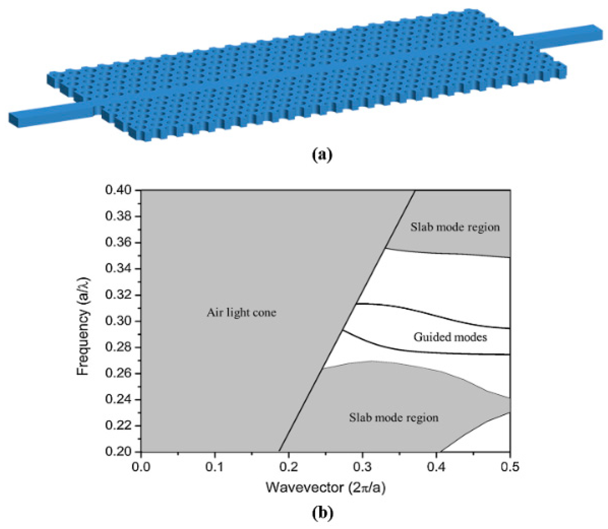
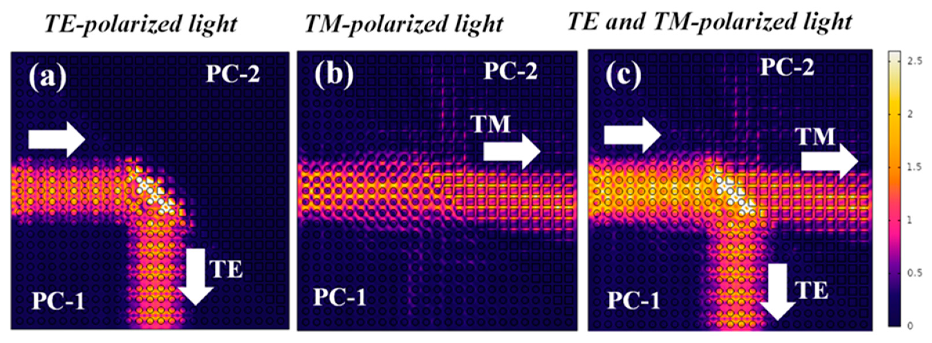
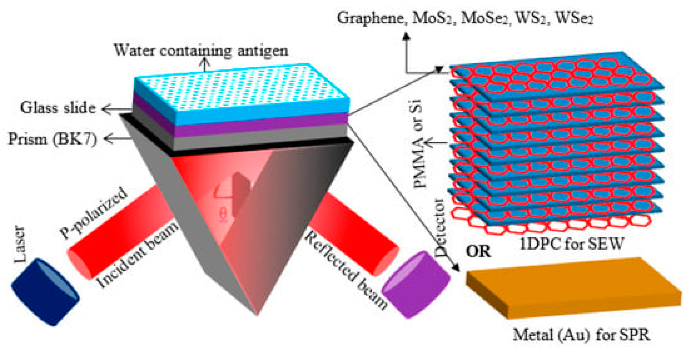
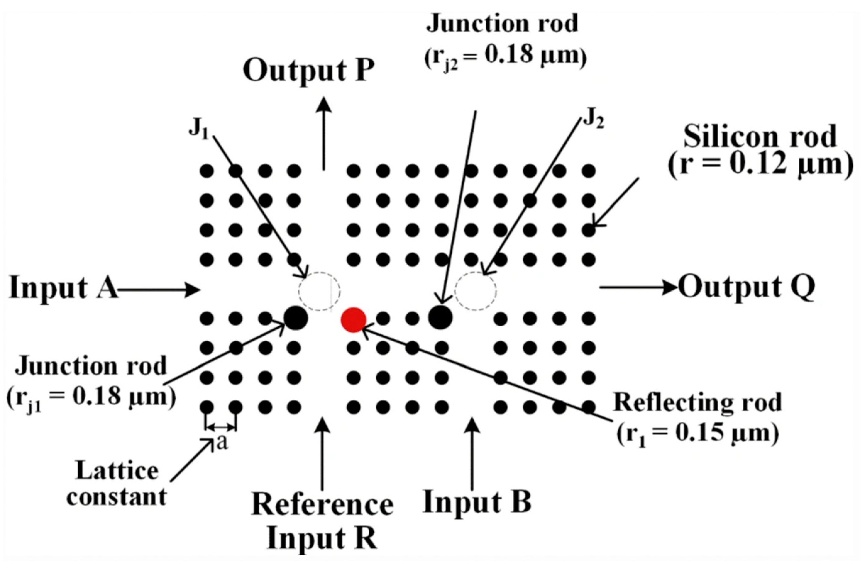
Table 1.
A summary of the PhC nanostructures utilized in photocatalytic degradation, PEC water splitting, and solar cells to improve their solar conversion efficiencies [74].
Table 1.
A summary of the PhC nanostructures utilized in photocatalytic degradation, PEC water splitting, and solar cells to improve their solar conversion efficiencies [74].
| Photonic Nanostructure | Material | Photocurrent Density | Power Conversion Efficiency | Reference |
|---|---|---|---|---|
| Microcavity | Fe2O3 | 0.35 at 1.23 VRHE | - | [75] |
| Cu2O/ZnO | 0.51 | [76] | ||
| TiO2 | - | [77] | ||
| Polymer solar cells | 4.5 | [78] | ||
| Semitransparent polymer | - | 24–27% | [79] | |
| WO3/Ag/WO3 | - | 8.37% | [80] | |
| PhC | TiO2/ZrO2 | - | - | [81] |
| BiVO4 | 1.35 at 1.2 V vs. Ag/AgCl | - | [82] | |
| Mo:BiVO4 | 2 at 1.0 V vs. Ag/AgCl | - | [83] | |
| Bi2WO6 | - | - | [84] | |
| WO3 | 2.5 at 1.0 V vs. SCE | - | [85] | |
| TiO2 nanodisk | - | 18.7%. | [86] | |
| Silicon | - | 31% | [87] | |
| CdS/TiO2 | 4.84 at 0 V vs. Ag/AgC | - | [88] | |
| PhC + Plasmon | Au/TiO2 | - | - | [89] |
| Au/TiO2 | - | - | [90] | |
| Au/BiVO4 | 3.1 at 1.23 VRHE | - | [91] | |
| TiO2/Au | - | 4.67 | [92] |
Table 2.
A summary of various PhC-based sensors, along with their sensing response and detection range.
Table 2.
A summary of various PhC-based sensors, along with their sensing response and detection range.
| Type of PhC | Sensing Material | Target | Detection Range | Sensitivity | Reference |
|---|---|---|---|---|---|
| Gas Sensors | |||||
| D shape fiber | Ag/Porous TiO2 | Isopropanol | 20–100% | 1.35 nm/% | [118] |
| PhC long-period grating | - | Methane | 0–3.5% | 6.39 nm/% | [119] |
| Microtube PhC | - | Propene | 33 vol% | 8.6–10.1% | [120] |
| hybrid porous core PCF | - | Methane | - | 21.2% | [121] |
| PC slab (PCS) | - | Carbon di oxide | 0–2130 ppm | - | [122] |
| 2D defect PCS | Polymer | Hexane and ethanol | 0–3 ppm | 123.4 nm/RIU | [123] |
| PhC cavity | - | Tetrahydrofuran | 0–31.5 mmol.L−1 | 0.128 nm·mmol.L−1 | [124] |
| PCF | NA | Sulfur Dioxide | 1.3406–1.3388 | 83.64% | [125] |
| PCF | - | Nitrous Oxide and Benzene | 1.295–1.3 | 73.822% 76.422% | [126] |
| Periodic PCS | Graphene | gas | - | - | [127] |
| 2D PhC | - | Sulfuric Acid and Hydrogen Peroxide | 0–90% | 575–600 nm/RIU | [128] |
| Physical sensor | |||||
| Bragg grating PhC | - | Temperature sensor | 5 °C–160 °C | 0.082 nm/°C | [129] |
| Dual-core PhC fiber | Fe3O4 | Magnetic field sensor | 89.9–271 Oe | 305.8 pm/Oe | [130] |
| Elliptical hole PhC Fiber | Platinum | Temperature sensor | 20–160 °C | 77 nm/°C | [131] |
| MMF-PCF | - | Strain sensor | 0–1600 με | ~−14.89 pm/με | [132] |
| D shaped PCF | Au film | Magnetic field and temperature sensor | 5 °C−65 °C 30 Oe~270 Oe | −1.25 nm/°C 0.21 nm/Oe | [133] |
| PhC | Self-adhesive hydrogel | Underwater motion detection | 0–200% | ≈2.09 nm/% | [134] |
| 2D PhC | GaAs | Pressure sensor | 0–5 GPa | 17.00 nm/GPa | [135] |
| PhC micro ring resonator | - | Pressure sensor | 0–0.5 GPa | 25.26 nm/GPa | [136] |
| 2D PhC | - | Pressure Sensor | 0–6 GPa | 3.1 nm/GPa | [137] |
| PCF | Silver | Temperature sensor | 15–35 °C | 2 nm/°C | [138] |
| Refractive index sensor | |||||
| D-shaped PhC Fiber | Gold film | Refractive index | 1.43–1.46 | 7700 nm/RIU | [139] |
| Dual drilled channel | Gold nanowire | Refractive index | 1.31–1.40 | 90,500 nm/RIU | [140] |
| H shaped fiber | Gold nanowire | Refractive index | 1.33–1.40 | 4000 nm/RIU | [141] |
| Tapered PCF | - | Bio-chemical | 1.30–1.32 | 722.3 nm/RIU | [142] |
| Hollow core | Cu nanowire | Refractive index | 1.33–1.38 | 12,400 nm/RIU | [143] |
| Hollow core PCF | - | Poisonous chemical | - | 92.08% | [144] |
| 2D PhC | - | Refractive index | 1.33–1.481 | 347.99–473.38 nm/RIU | [145] |
| Single channel PCF | - | Petrol adulteration | 1.415–1.440 | 20,161.2 nm/RIU | [146] |
| 1D defect PhC | Superconducting material | Biosensing | 0–50% | 68.18–85.22 nm/RIU | [147] |
| 1D PhC | - | Hemoglobin | 10–150 g/L | 1916.77 nm/RIU | [148] |
| 2D PCF | Au film | Protein | 0–10 μg/L | 10−3 μg/mL | [149] |
Disclaimer/Publisher’s Note: The statements, opinions and data contained in all publications are solely those of the individual author(s) and contributor(s) and not of MDPI and/or the editor(s). MDPI and/or the editor(s) disclaim responsibility for any injury to people or property resulting from any ideas, methods, instructions or products referred to in the content. |
© 2023 by the authors. Licensee MDPI, Basel, Switzerland. This article is an open access article distributed under the terms and conditions of the Creative Commons Attribution (CC BY) license (https://creativecommons.org/licenses/by/4.0/).
Share and Cite
MDPI and ACS Style
Gangwar, R.K.; Pathak, A.K.; Kumar, S. Recent Progress in Photonic Crystal Devices and Their Applications: A Review. Photonics 2023, 10, 1199. https://0-doi-org.brum.beds.ac.uk/10.3390/photonics10111199
AMA Style
Gangwar RK, Pathak AK, Kumar S. Recent Progress in Photonic Crystal Devices and Their Applications: A Review. Photonics. 2023; 10(11):1199. https://0-doi-org.brum.beds.ac.uk/10.3390/photonics10111199
Chicago/Turabian StyleGangwar, Rahul Kumar, Akhilesh Kumar Pathak, and Santosh Kumar. 2023. "Recent Progress in Photonic Crystal Devices and Their Applications: A Review" Photonics 10, no. 11: 1199. https://0-doi-org.brum.beds.ac.uk/10.3390/photonics10111199
Note that from the first issue of 2016, this journal uses article numbers instead of page numbers. See further details here.