Article

Cap Layer Effect on Key Features of Persistent Photoconductivity Spectra in HgTe/CdHgTe Double Quantum Well Heterostructures

by
Mikhail K. Sotnichuk
1,
Aleksei S. Kazakov
1,
Ilya D. Nikolaev
1,
Konstantin A. Drozdov
1,
Roman V. Menshchikov
2,
Sergey A. Dvoretsky
2,
Nikolay N. Mikhailov
2,
Dmitry R. Khokhlov
1 and
Anton V. Ikonnikov
1,*
1
Faculty of Physics, Lomonosov Moscow State University, 119991 Moscow, Russia
2
Rzhanov Institute of Semiconductor Physics, Siberian Branch, Russian Academy of Sciences, 630090 Novosibirsk, Russia
*
Author to whom correspondence should be addressed.
Submission received: 1 July 2023 / Revised: 22 July 2023 / Accepted: 25 July 2023 / Published: 28 July 2023

Abstract

:
Persistent photoconductivity (PPC) spectra of HgTe/CdHgTe heterostructures with double quantum wells with different cap layers have been studied in the radiation excitation range 0.62–3.1 eV. We have shown that the material of the cap layer defines key features of the PPC spectra—local extrema—and their origin. An unusual oscillatory behavior of the PPC spectra is demonstrated. Such a behavior is shown to be independent of both cap and barrier layers.

1. Introduction

The phenomenon of persistent photoconductivity, i.e., the effect that occurs when the conductivity change persists after turning the radiation off, has been known for decades. This effect is often used as an effective and simple method for controlling the concentration of charge carriers. PPC can be observed both in bulk semiconductors [1,2,3,4] and in low-dimensional structures [5,6,7,8,9,10,11,12,13,14,15,16]. In most cases, positive PPC takes place, which means that the carrier concentration (and, accordingly, conductivity) increases when the illumination is turned on. For example, in GaAs/AlGaAs heterostructures, the concentration of electrons may increase by 2–2.5 times when the sample is illuminated with light in the visible or near-infrared range [7]. Another type of this effect is negative PPC, which corresponds to a decrease in charge carrier concentration [8,9,10] under the influence of radiation. The PPC sign may depend on the structure’s composition and the doping type as well as on the incident radiation. In the latter case, the conductivity of a structure may be increased or decreased depending on the wavelength of the incident light. This type of PPC is called bipolar and has the most practical interest. Bipolar PPC has been observed in, for example, InAs/AlSb heterostructures [11,12,13] and HgTe/CdHgTe heterostructures [14,15,16].
HgTe/CdHgTe heterostructures are the subject of intense research since they are the first experimentally discovered two-dimensional topological insulators [17]. In such systems, the edge conductive states exist protected from scattering due to the time-reversal symmetry. These states contribute to the conductivity even when bulk conductivity is suppressed. At the same time, HgTe/CdHgTe heterostructures with double quantum wells (DQWs) are of particular interest since they have more options for controlling the band structure by changing the thicknesses of QWs and the barrier height between them. They also provide a greater variety of topological phases compared to single HgTe/CdHgTe QWs [18]. In particular, unique topological phases can appear in DQWs, such as the “double inversion” phase, in which the system can be considered as a higher order topological insulator [19]. The latter is currently a hot topic in the physics of topologically non-trivial systems [20,21,22].
Transport methods may be informative for studying various topological phases and observing topological conducting edge states [17,23,24]. On the other hand, bulk conductivity should be excluded in order to observe the edge states. This means that it is necessary to control the Fermi level position. In most cases, this is achieved by fabricating gated structures. Another way of controlling the carrier concentration is utilization of the PPC effect. In this respect, HgTe/CdHgTe heterostructures with DQWs look like very suitable objects for research. They demonstrate not only an ability to decrease or increase the carrier concentration after illumination, but also the possibility of a reversible change in the conductivity type [16].
To date, PPC in HgTe/CdHgTe heterostructures with DQWs has been studied in detail only in [15,16]. In these two papers, the presence of the bipolar PPC was demonstrated, the main features of the PPC spectra were detected, and the main reasons for their appearance were identified. It was found that the resistance value established after illumination is determined primarily by the concentration and type of charge carriers. The mentioned parameters, in turn, are determined by the balance between the generation and recombination of electrons and holes, as well as their drift and diffusion in the QW. In addition, the effect of the CdTe cap layer on key features of the PPC spectra was noted. Finally, an optimal method for controlling the carrier concentration, which is related to the energy parameters of the cap layer, was suggested [16].
In this paper, we directly demonstrate the effect of the cap layer on PPC spectra studying HgTe/CdHgTe DQW heterostructures with different cap layers. We carried out PPC spectra measurements in the wavelength range of 400–2000 nm at two different temperatures. It was shown that the key features of the PPC spectra are determined by the cap layer.

2. Materials and Methods

2.1. Samples under Study

The structures under study were grown by molecular beam epitaxy on semi-insulating GaAs substrates [25]. First, a thin (30 nm) ZnTe spacer was grown followed by a thick (~5 μm) relaxed CdTe buffer layer, and then by the structure’s active part. The latter consisted of a lower 30 nm thick CdxHg1–xTe barrier layer, two HgTe or Hg1–yCdyTe QWs with a width d separated by a tunnel-transparent CdxHg1–xTe barrier with a thickness t, and an upper 30 nm thick CdxHg1–xTe barrier. Finally, a cap layer was grown over the active part, and for all the structures this layer was different. The structures were not intentionally doped. For studying the PPC spectra, as well as for carrying out transport measurements, 4 × 5 mm samples with indium contacts deposited according to the Hall geometry were prepared. The sample parameters are given in Table 1. The structure parameters were chosen to provide the direct band spectrum [18]. The structure composition was controlled in situ using ellipsometry [25].

2.2. PPC Spectra Measurements

The PPC spectra were measured in the wavelength range 400–2000 nm (corresponding to the energy range 0.62–3.1 eV) using a grating monochromator MDR-206 with a sweep rate of 5 or 10 nm/min at T = 4.2 K and T = 77 K. The sweep rate values were chosen to provide insignificant change in the incident radiation wavelength during the time needed for the sample resistance to reach saturation. The chosen energy range was determined, firstly, by the characteristic interband energies of the heterostructures under study (see energy diagrams below) and, secondly, by the 600 lines/mm diffraction grating used. Optical filters were installed at the monochromator output to eliminate the influence of second and higher order diffraction. For the measurements, the sample was placed at the end of a special insert, which was a metal tube polished from the inside. The insert with the sample was placed in a helium or nitrogen Dewar. The light from the monochromator was guided towards the sample through a quartz input window along a polished tube. The sample resistance was measured using the four-probe method. The sample current was in the range from 0.1 to 10 μA. The dependence of the sample resistance on the incident radiation wavelength was taken. The scanning direction (from shorter to longer wavelengths and vice versa) did not significantly affect the PPC spectral features.

2.3. Resistance Kinetics Measurements and Magnetotransport Measurements

To determine the dependence of the carrier concentration in the DQW on the wavelength of the incident radiation, point-by-point measurements of the Hall effect and Shubnikov–de Haas oscillations were carried out. During the measurements, the insert with the sample was placed in a liquid helium cryostat, which contained a superconducting solenoid generating a magnetic field up to 5 T. The longitudinal (Rxx) and Hall (Rxy) resistances were measured. The sample was illuminated by radiation with a given wavelength until the resistance reached a quasi-equilibrium value. Then the illumination was turned off, and after a ‘new’ resistance value was established, magnetotransport measurements were performed. The characteristic mobilities after illumination for samples A and B were about 5 × 104 cm2/V·s and 103 cm2/V·s, respectively. For sample C, the mobility could not be reliably determined.
During the illumination of the sample and after it was turned off, the resistance kinetics of the sample were recorded. A typical kinetics example is shown in the inset in Figure 1a. The resistance values established after illumination (point-by-point recording) were in good agreement with the resistance values obtained while recording the PPC spectra (continuous recording), which indicates the presence of a pronounced PPC effect.

2.4. Energy Diagram Calculations

Energy diagrams of all the structures under study were calculated in order to interpret the measured PPC spectra. The values of the CdxHg1–xTe bandgap were calculated using the Lorenti formula [26], whereas the value of the ZnTe bandgap was taken from [27]. The valence band offset at the CdTe–HgTe heterointerface and the positions of the spin-split band for pure CdTe and HgTe were taken from [28], the same values for ZnTe were taken from [29]. For CdHgTe solid solutions, the values were obtained by linear interpolation. The resulting diagrams for all samples are shown in Figure 1d–f.

3. Results and Discussion

3.1. Key Features of the PPC Spectra

Figure 1 shows the measured PPC spectra, as well as calculated band diagrams, for all the structures under study. We will start by discussing results from the “reference” sample, A. This sample has an electron conductivity type in the entire range of the incident radiation quantum energies used. The cap layer of this sample is CdTe, which is traditional for heterostructures based on CdHgTe. The same structure was studied in [16]. In the PPC spectrum (Figure 1a) measured at T = 4.2 K, two main features are observed. Feature 1 is a sharp drop in resistance near the energy of 1.55 eV, whereas feature 2 is a local resistance maximum at the photon energy of 2.42 eV. As already noted in the Introduction, the resistance value established after illumination is determined by a certain balance of the processes responsible for increasing and decreasing the number of electrons or holes in the QW. When considering sample A, this makes it possible to state that appearance of the feature 1 is related to “switching on” generation of electron-hole pairs in the CdTe cap layer (Figure 1d). This process shifts the balance in such a way that the number of electrons entering the QW increases, and the sample resistance decreases accordingly. In addition, the generation of electron-hole pairs in the CdTe buffer layer can also make a small contribution. Moving on to the discussion of feature 2, we, following the authors of [16], state that it appears due to the transitions between the spin-split band of the Cd0.65Hg0.35Te barrier layer and the conduction band of the CdTe cap layer (Figure 1d). The mentioned process increases the number of holes reaching the QW, so that the sample resistance increases. The energy position of feature 1 is somewhat smaller than the CdTe bandgap (1.55 eV versus 1.6 eV), which is caused by the penetration of mercury atoms from the Cd0.65Hg0.35Te barrier layer into the cap layer, which leads to a decrease in the bandgap.
An increase in temperature to T = 77 K leads to a small shift of the features’ positions towards lower energies. This shift takes place due to a slight (~1%) decrease in the band gaps of the cap and barrier layers [26].
Next, we will discuss results obtained for sample B with the ZnTe cap layer. Like the “reference” sample, A, it has the electronic type of conductivity in the entire range of incident photon energies used in our measurements (Figure 1b). Just as in the case of sample A, the conductivity and resistance are completely determined by the electron density in the DQW (see Figure 1 in [16]). This statement is confirmed by magnetotransport measurements carried out after the illumination with a given photon energy is turned off. As can be seen from Figure 1b, an increase in resistance is accompanied by a decrease in the electron concentration and vice versa. At the same time, an increase (decrease) in concentration is also accompanied by a corresponding increase (decrease) in mobility, which means that both factors have the same influence on the resistance of the sample. There is a good correspondence between the PPC spectra measured during continuous scanning and the dependence of the concentration on the incident photon energy, obtained during point-by-point scanning. This fact proves that persistent photoconductivity indeed has the greatest effect on the obtained spectra.
The replacement of the CdTe cap layer with ZnTe in sample B leads to a qualitative change in the PPC spectra (Figure 1b). In the PPC spectra of sample A, feature 1 is observed, which is a sharp resistance drop near the incident photon energy of 1.55 eV. On the other hand, there is only a small minimum at the same quantum energy (feature 3) in the spectra of sample B. We believe that feature 3 appears due to the generation of electron-hole pairs in the CdTe buffer layer, which leads to a slight shift in the balance and an increase in the number of electrons reaching the QW.
Feature 2 is not observed in the PPC spectra of sample B. The resistance maximum at the energy of 2.25 eV cannot be associated with transitions from the spin-split band of the CdHgTe barrier to the conduction band of the ZnTe cap layer, as the energy of this transition should be about 2.9 eV (Figure 1e). It also cannot appear as a result of transitions to the conduction band of the CdTe buffer layer, because the energy of this transition should practically coincide with the position of feature 2 in sample A (2.4 eV), since the barrier compositions in samples A and B are almost identical.
The bandgap of ZnTe is 2.39 eV at T = 4.2 K, so it is possible to state that the resistance maximum observed in the PPC spectrum of sample B at the energy of 2.25 eV, and the subsequent decrease in resistance, are related to the activation of electron-hole pair generation in the ZnTe cap layer, in an analogy with sample A. However, in contrast to sample A, turning the generation on in the cap layer leads not to a sharp, but to a smooth, decrease in the resistance (feature 1 in Figure 1b). Apparently, this happens due to the penetration of both mercury and cadmium atoms from the barrier layer into the ZnTe cap layer, which can lead to strong inhomogeneities (they appear because mercury diffuses more strongly) and blurring of the absorption edge. This also causes a decrease in the bandgap of the cap layer, at least in some areas, and, consequently, a shift in the resistance maximum (2.25 eV) relative to the band gap of “pure” ZnTe (2.39 eV). Strong blurring of feature 1 can also mask feature 2, or at least make it less clear. Increasing the temperature to T = 77 K logically leads to a resistance maximum shift towards lower energies.
In the PPC spectra of sample C, almost the same features as in samples A and B are observed (Figure 1c). Feature 1, which is a sharp resistance drop at the energy of 1.15 eV, is similar to the sharp drop at 1.55 eV in sample A. It is natural to associate the appearance of this feature with “switching on” the interband transitions in the CdxHg1–xTe cap layer. The position of feature 1 corresponds well to the band gap of a solid solution with the cadmium fraction x = 0.78 (Figure 1c), although this value is slightly less than the nominal cap layer cadmium fraction x = 0.85. Such a decrease in the cadmium fraction (and, hence, an increase in the mercury fraction) may be caused by the penetration of mercury atoms from the CdHgTe barrier layer during the structure growth.
Feature 2 in sample C is a local resistance minimum at 2 eV (Figure 1c), in contrast to the peaks in samples A (Figure 1a) and B (Figure 1b). As in [16], we assume that this feature appears due to transitions between the spin-split band of the Cd0.66Hg0.34Te barrier layer and the conduction band of the Cd0.78Hg0.22Te cap layer (Figure 1f). The energy position of this feature agrees well with the energy of this transition. As mentioned earlier, such a transition increases the number of holes entering the QWs, which causes an increase in resistance in samples with the n-type conductivity (in our case, these are samples A and B) in the considered energy range, and a decrease in resistance in samples with the p-type conductivity (in our case, sample C). The same behavior for samples with different conductivity types was demonstrated in [16].
Feature 2′, which is a drop at the energy of 2.38 eV (Figure 1c), is similar to feature 2. We associate feature 2′ with transitions between the spin-split band of the Cd0.66Hg0.34Te barrier layer and the conduction band of the CdTe buffer layer. The energy of such transitions exactly coincides with the position of feature 2′.
When the temperature is increased to T = 77 K, a slight shift in the spectral position of features 2 and 2′ towards lower energies can be observed (Figure 1c), just like for samples A and B. This is associated with a decrease in the band gaps of the cap layer and the CdHgTe barriers. At the same time, a significant (0.1 eV) shift in the feature 1 position towards lower energies turned out to be unexpected. This shift cannot be caused only by a decrease in the band gap of the Cd0.78Hg0.22Te cap layer and requires additional checks. In addition, there is a resistance peak at 1.55 eV, which is very close to the band gap of CdTe. This peak may be similar to feature 3 in sample B and its appearance may be associated with the electron-hole pair generation in the CdTe buffer layer. However, this statement also requires additional verification.
Finally, the local maxima or minima observed in the PPC spectra of all samples at low energies (E < 1–1.2 eV) (Figure 1a–c) do not have a clear association with the characteristics of the energy diagrams (Figure 1d–f). Most likely, they are related to transitions to or from some deep impurity centers in the cap or barrier layers or with the individual features of the samples (cf. Figure 2a in [16] and the corresponding explanation).

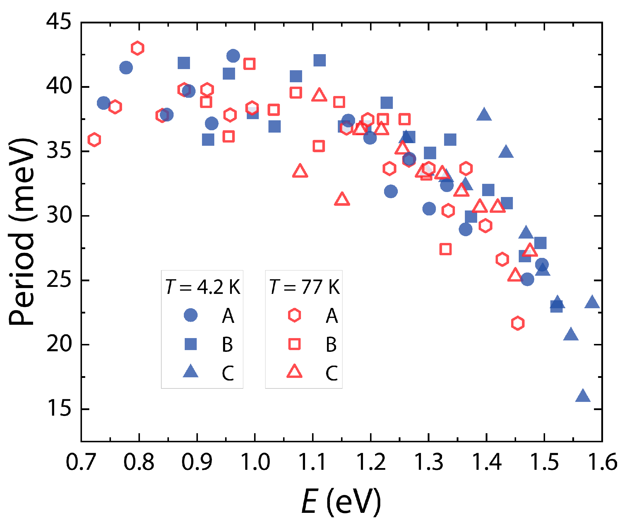
3.2. Oscillations in the PPC Spectra

In all samples at all temperatures, an oscillatory change in resistance with increasing photon energy in the range from 0.7–0.9 eV to 1.5–1.6 eV was observed (Figure 1a–c). The most evident oscillations are present in the PPC spectra of sample B (Figure 1b). Figure 2 shows the dependence of the oscillation period on the energy at which a resistance minimum of a particular oscillation is observed. The spread of values is, first of all, determined by a random error that occurs when subtracting the baseline and choosing the position of a specific minimum. It can be seen that all dependences for different samples and different temperatures have the same trend. Specifically, in the long-wavelength region, the oscillation period remains practically unchanged and is equal to about 40 meV, and then, starting from energies of ~1.1 eV, it starts to decrease, reaching 15–20 meV in the short-wavelength region.
A similar oscillatory behavior of the conductivity in the PPC spectra was also observed for another InAs/AlSb heterosystem [11,12]. However, a comprehensive explanation of this phenomenon has not yet been presented. The authors of [11] associated these oscillations with the emission of a longitudinal optical phonon cascade. Phonons, in this case, were emitted by light holes which were excited during direct optical transitions in the GaSb cap layer and then injected into the AlSb barrier. The observed period of oscillations in the long-wavelength region (~80 meV) was approximately double (due to the closeness effective masses of the electrons and light holes) the energy of the optical phonon in AlSb. A decrease in the oscillation period to 50 meV in the short-wavelength region was associated with an increase in the effective electron mass due to the non-parabolic dispersion law. However, in [12], for similar InAs/AlSb structures, a significantly shorter oscillation period was observed (~50 meV in the long-wavelength region and ~40 meV in the short-wavelength region). This made the authors of [12] conclude that the mechanism discussed above was not suitable for explaining the oscillation appearance. They proposed another mechanism—the interband excitation of electrons into higher subbands in the InAs quantum well, followed by their capture by ionized deep donor centers in barrier layers.
Our studies do not demonstrate any correlation between the dependences of the oscillation periods and heterostructure composition. It can be noticed that the dependences are similar for all the samples under study (Figure 2). Moreover, an additional study of oscillations in the PPC spectra of HgTe/CdHgTe DQWs with x = 0.34 in the CdxHg1–xTe barrier layers demonstrated the same dependence. This means that the oscillations cannot be associated with the cap or barrier layers. In addition, they cannot be associated with a Fabry–Perot resonator formed by structure layers. In this case, the oscillation period should remain practically unchanged (the refractive index of the layer materials in the considered range changes by no more than 10% [30]), which is not observed. Thus, oscillations can be associated either with the CdTe buffer layer, or with the HgTe QWs themselves, or with something else. Revealing the specific reason for the oscillation appearance in the PPC spectra requires additional studies.

4. Conclusions

The PPC spectra of HgTe/CdHgTe DQWs with different cap layers were studied in the incident photon energy range of 0.62–3.1 eV. Oscillatory dependence of the resistance in the energy range of 0.7–1.6 eV was observed in the PPC spectra. The appearance of such oscillations is not related to the cap layer.
In addition, three main features were distinguished in the PPC spectra of the structures under study. They are associated with the interband generation of electron-hole pairs in the cap layer (feature 1), transitions from the spin-split band to the conduction band of the cap layer (feature 2), and interband generation in the CdTe buffer layer (feature 3). The spectral positions of the dominant features, 1 and 2, depend on the cap layer material: when a narrower band material is used, a red shift in the feature positions takes place.
Thus, the replacement of the cap layer material in HgTe/CdHgTe heterostructures with DQWs leads to a qualitative change in the PPC spectra and has a significant effect on the key features of the spectra.

Author Contributions

Conceptualization, A.V.I.; methodology, A.V.I. and K.A.D.; software, M.K.S.; validation, A.V.I. and I.D.N.; formal analysis, M.K.S. and A.V.I.; investigation, M.K.S.; resources, R.V.M., S.A.D. and N.N.M.; data curation, M.K.S. and A.V.I.; writing—original draft preparation, M.K.S., A.S.K. and A.V.I.; writing—review and editing, K.A.D., I.D.N. and D.R.K.; visualization, A.V.I.; supervision, D.R.K. and A.V.I.; project administration, A.V.I.; funding acquisition, A.V.I. All authors have read and agreed to the published version of the manuscript.

Funding

This work was supported by the Russian Science Foundation (Grant No. 22-22-00382).

Institutional Review Board Statement

Not applicable.

Informed Consent Statement

Not applicable.

Data Availability Statement

The data presented in this study are available on request from the corresponding author.

Conflicts of Interest

The authors declare no conflict of interest.

References

  1. Wright, H.C.; Downey, R.J.; Canning, J.R. Conductivity storage in CdS. J. Phys. D Appl. Phys. 1968, 1, 1593. [Google Scholar] [CrossRef]
  2. Lang, D.V.; Logan, R.A.; Jaros, M. Trapping characteristics and a donor-complex (DX) model for the persistent-photoconductivity trapping center in Te-doped AlxGa1−xAs. Phys. Rev. B 1979, 19, 1015. [Google Scholar] [CrossRef]
  3. Akimov, B.A.; Brandt, N.B.; Gas’kov, A.M.; Zlomanov, V.P.; Ryabova, L.I.; Khokhlov, D.R. Gallium impurity states and photoelectric phenomena in PbTe-Ga alloys. Sov. Phys. Semicond. 1983, 17, 53. [Google Scholar]
  4. Hirsch, M.T.; Wolk, J.A.; Walukiewicz, W.; Haller, E.E. Persistent photoconductivity in n-type GaN. Appl. Phys. Lett. 1997, 71, 1098. [Google Scholar] [CrossRef]
  5. Tsai, L.C.; Huang, C.F.; Fan, J.C.; Chang, Y.H.; Chen, Y.F.; Tsai, W.C.; Chang, C.Y. Persistent photoconductivity in SiGe/Si quantum wells. J. Appl. Phys. 1998, 84, 877. [Google Scholar] [CrossRef]
  6. Anderson, D.A.; Bass, S.J.; Kane, M.J.; Taylor, L.L. Transport and persistent photoconductivity in InGaAs/InP single quantum wells. Appl. Phys. Lett. 1986, 49, 1360. [Google Scholar] [CrossRef]
  7. Kastalsky, A.; Hwang, J.C.M. Study of persistent photoconductivity effect in n-type selectively doped AlGaAs/GaAs heterojunction. Solid State Commun. 1984, 51, 317. [Google Scholar] [CrossRef]
  8. Chen, J.; Yang, C.H.; Wilson, R.A.; Yang, M.J. Observation of negative persistent photoconductivity in an n-channel GaAs/AlxGa1−xAs single heterojunction. Appl. Phys. Lett. 1992, 60, 2113. [Google Scholar] [CrossRef]
  9. Lo, I.; Mitchel, W.C.; Manasreh, M.O.; Stutz, C.E.; Evans, K.R. Negative persistent photoconductivity in the Al0.6Ga0.4Sb/InAs quantum wells. Appl. Phys. Lett. 1992, 60, 751. [Google Scholar] [CrossRef]
  10. Chaves, A.S.; Chacham, H. Negative photoconductivity in semiconductor heterostructures. Appl. Phys. Lett. 1995, 66, 727. [Google Scholar] [CrossRef]
  11. Gauer, C.; Scriba, J.; Wixforth, A.A.; Kotthaus, J.P.; Nguyen, C.; Tuttle, G.; English, J.H.; Kroemer, H. Photoconductivity in AlSb/InAs quantum wells. Semicond. Sci. Technol. 1993, 8, S137. [Google Scholar] [CrossRef]
  12. Aleshkin, V.Y.; Gavrilenko, V.I.; Gaponova, D.M.; Ikonnikov, A.V.; Marem’yanin, K.V.; Morozov, S.V.; Sadofyev, Y.G.; Johnson, S.R.; Zhang, Y.H. Spectra of persistent photoconductivity in InAs/AlSb quantum-well heterostructures. Semiconductors 2005, 39, 22. [Google Scholar] [CrossRef]
  13. Gavrilenko, V.I.; Ikonnikov, A.V.; Krishtopenko, S.S.; Lastovkin, A.A.; Marem’yanin, K.V.; Sadofyev, Y.G.; Spirin, K.E. Persistent photoconductivity in InAs/AlSb heterostructures with double quantum wells. Semiconductors 2010, 44, 616. [Google Scholar] [CrossRef]
  14. Spirin, K.E.; Gaponova, D.M.; Gavrilenko, V.I.; Mikhailov, N.N.; Dvoretsky, S.A. Residual-photoconductivity spectra in HgTe/CdHgTe quantum-well heterostructures. Semiconductors 2019, 53, 1363. [Google Scholar] [CrossRef]
  15. Spirin, K.E.; Gaponova, D.M.; Marem’yanin, K.V.; Rumyantsev, V.V.; Gavrilenko, V.I.; Mikhailov, N.N.; Dvoretsky, S.A. Bipolar persistent photoconductivity in HgTe/CdHgTe (013) double quantum-well heterostructures. Semiconductors 2018, 52, 1586. [Google Scholar] [CrossRef]
  16. Nikolaev, I.D.; Kazakov, A.S.; Drozdov, K.A.; Bannikov, M.I.; Spirin, K.E.; Menshchikov, R.V.; Dvoretsky, S.A.; Mikhailov, N.N.; Khokhlov, D.R.; Ikonnikov, A.V. Bipolar persistent photoconductivity in HgTe/CdHgTe double quantum well heterostructures and its application for reversible change in the conductivity type. J. Appl. Phys. 2022, 132, 234301. [Google Scholar] [CrossRef]
  17. König, M.; Wiedmann, S.; Brüne, C.; Roth, A.; Buhmann, H.; Molenkamp, L.W.; Qi, X.-L.; Zhang, S.-C. Quantum spin Hall insulator state in HgTe quantum wells. Science 2007, 318, 766. [Google Scholar] [CrossRef] [Green Version]
  18. Krishtopenko, S.S.; Knap, W.; Teppe, F. Phase transitions in two tunnel-coupled HgTe quantum wells: Bilayer graphene analogy and beyond. Sci. Rep. 2016, 6, 30755. [Google Scholar] [CrossRef] [Green Version]
  19. Krishtopenko, S.S. Higher-order topological insulator in cubic semiconductor quantum wells. Sci. Rep. 2021, 11, 21060. [Google Scholar] [CrossRef]
  20. Schindler, F.; Cook, A.M.; Vergniory, M.G.; Wang, Z.; Parkin, S.S.; Bernevig, B.A.; Neupert, T. Higher-order topological insulators. Science advances. Sci. Adv. 2018, 4, eaat0346. [Google Scholar] [CrossRef] [Green Version]
  21. Kim, M.; Jacob, Z.; Rho, J. Recent advances in 2D, 3D and higher-order topological photonics. Light Sci. Appl. 2020, 9, 130. [Google Scholar] [CrossRef] [PubMed]
  22. Xie, B.; Wang, H.X.; Zhang, X.; Zhan, P.; Jiang, J.H.; Lu, M.; Chen, Y. Higher-order band topology. Nat. Rev. Phys. 2021, 3, 520. [Google Scholar] [CrossRef]
  23. Lunczer, L.; Leubner, P.; Endres, M.; Müller, V.L.; Brüne, C.; Buhmann, H.; Molenkamp, L.W. Approaching quantization in macroscopic quantum spin Hall devices through gate training. Phys. Rev. Lett. 2019, 123, 047701. [Google Scholar] [CrossRef] [PubMed] [Green Version]
  24. Gusev, G.M.; Olshanetsky, E.B.; Hernandez, F.G.G.; Raichev, O.E.; Mikhailov, N.N.; Dvoretsky, S.A. Two-dimensional topological insulator state in double HgTe quantum well. Phys. Rev. B 2020, 101, 241302. [Google Scholar] [CrossRef]
  25. Mikhailov, N.N.; Smirnov, R.N.; Dvoretsky, S.A.; Sidorov, Y.G.; Shvets, V.A.; Spesivtsev, E.V.; Rykhlitski, S.V. Growth of Hg1–xCdxTe nanostructures by molecular beam epitaxy with ellipsometric control. Int. J. Nanotechnol. 2006, 3, 120. [Google Scholar] [CrossRef]
  26. Laurenti, J.P.; Camassel, J.; Bouhemadou, A.; Toulouse, B.; Legros, R.; Lusson, A. Temperature dependence of the fundamental absorption edge of mercury cadmium telluride. J. Appl. Phys. 1990, 67, 6454. [Google Scholar] [CrossRef]
  27. Rogalsky, A. Hg1-xZnxTe as a potential infrared detector material. Prog. Quant. Electr. 1989, 13, 299. [Google Scholar] [CrossRef]
  28. Novik, G.; Pfeuffer-Jeschke, A.; Jungwirth, T.; Latussek, V.; Becker, C.R.; Landwehr, G.; Buhmann, H.; Molenkamp, L.W. Band structure of semimagnetic Hg1–yMnyTe quantum well. Phys. Rev. B 2005, 72, 035321. [Google Scholar] [CrossRef] [Green Version]
  29. Grinyaev, S.N.; Kataev, S.G. Electronic structure of ZnxCdyHg1-x-yTe alloys and related heterojunctions. Phys. B Condens. Matter 1993, 191, 317. [Google Scholar] [CrossRef]
  30. Marple, D.T.F. Refractive index of ZnSe, ZnTe, and CdTe. J. Appl. Phys. 1964, 35, 539. [Google Scholar] [CrossRef]
Figure 1. Left panel: dependence of the resistance on the incident photon energy obtained at two different temperatures during continuous scanning in samples A (a), B (b), C (c). For sample B (b), dependence of the electron concentration on the energy of the incident photon is shown as well. It was obtained by point-by-point scanning at T = 4.2 K. The vertical lines indicate the band gaps of CdTe, ZnTe, and Cd0.78Hg0.22Te at T = 4.2 K; the numbers indicate the observed spectral features. The inset shows the kinetics of the resistance change in sample A after turning off illumination with a photon energy of 2.7 eV and then turning on illumination with a photon energy of 3.02 eV. Horizontal lines denote the established resistance values. Right panel: energy diagrams of samples A (d), B (e), C (f). The energies are given in meV. The GaAs substrate is located on the right side (not shown in the figure). The vertical lines indicate the transitions associated with the key features of the spectra.
Photonics 10 00877 g001aPhotonics 10 00877 g001b
Figure 2. Dependences of the oscillation period on the energy at which a resistance minimum of a particular oscillation is observed.
Photonics 10 00877 g002
Table 1. Growth parameters of the structures and the resistance values before illumination.
SampleNo.d, nmt, nmx, %y, %Cap LayerR4.2 K, kOhmR77 K, kOhm
A1703206.5365~8CdTe0.582.17
B22091243630ZnTe12123.6
C22090943660Cd0.85Hg0.15Te107140
Disclaimer/Publisher’s Note: The statements, opinions and data contained in all publications are solely those of the individual author(s) and contributor(s) and not of MDPI and/or the editor(s). MDPI and/or the editor(s) disclaim responsibility for any injury to people or property resulting from any ideas, methods, instructions or products referred to in the content.

