Spontaneous Emission Studies for Blue and Green InGaN-Based Light-Emitting Diodes and Laser Diodes


1
Department of Nano & Semiconductor Engineering, Tech University of Korea, Siheung 15073, Republic of Korea
2
Department of Materials Science and Engineering, Inha Technical College, Incheon 22212, Republic of Korea
*
Author to whom correspondence should be addressed.
Photonics 2024, 11(2), 135; https://0-doi-org.brum.beds.ac.uk/10.3390/photonics11020135
Submission received: 4 January 2024
/
Revised: 25 January 2024
/
Accepted: 30 January 2024
/
Published: 31 January 2024
(This article belongs to the Special Issue Photodetector Materials and Optoelectronic Devices)
Abstract
:We investigated the efficiency droop phenomenon in blue and green GaN-based light-emitting diodes (LEDs) and laser diodes (LDs), which poses a significant challenge in high-power LEDs and is characterized by a reduction in external quantum efficiency at higher injection currents. Utilizing identical epi-structures for blue and green LEDs and LDs, with variations only in indium composition, our experiments revealed a gradual blue shift in the emission wavelengths as the injection current increased. Notably, the blue LED demonstrated a smaller shift compared to the green LED. In addition, the full width at half maximum of emission spectra increased with increasing injection current density, indicative of efficiency droop. Significantly, LDs consistently exhibited lower junction temperatures despite operating at higher current densities. This is attributed to the enhanced heat dissipation capability of the ridge waveguide LD structure, which results in a narrower emission spectrum and reduced efficiency droop compared to mesa LED structures. These outcomes highlight the efficiency of the ridge waveguide LD structure in heat dissipation from the active layer, offering crucial insights for the advancement of high-power light-emitting devices.
1. Introduction
III-nitride semiconductors have attracted significant interest in high-performance optoelectronic devices, such as light-emitting diodes (LEDs) and laser diodes (LDs), due to their wide bandgap and superior physical and chemical properties [1,2,3,4]. High-power GaN-based blue, green, and white LEDs are extensively used in applications like backlighting and solid-state lighting. Moreover, violet to green GaN-based LDs are pivotal in high-data storage and laser displays as coherent light sources [3,4]. Despite their widespread applications, achieving high-performance, longer-wavelength green and red light-emitting devices remains a challenge [4,5,6]. This is primarily due to material limitations, including the large lattice mismatch and miscibility gap within the InN-GaN system [7,8]. The stimulated emission of green LDs is particularly challenging, hindered by high indium composition in InGaN materials, which leads to issues like indium segregation and strong piezoelectric fields [8,9]. Consequently, green light-emitting devices, compared to their blue counterparts, face significant challenges in enhancing output power, notably the efficiency droop—a phenomenon where there is a gradual reduction in external quantum efficiency with increasing injection current [10,11]. Addressing these challenges is vital for advancing the performance and broadening the applications of green light-emitting devices across various technology sectors.
Efficiency droop in GaN-based light-emitting devices remains a complex and partially understood phenomenon, with multiple proposed causes such as carrier leakage, junction heating, Auger recombination, and carrier delocalization [11,12,13,14]. Despite a range of theories, contentious aspects of interpreting efficiency droop still exist. Prior studies have identified factors like Auger recombination, carrier overflow, leakage currents, and p-n junction temperature as contributing to efficiency droop. To uncover the root causes, we adopted a consistent epitaxial structure for both blue or green GaN-based light-emitting devices, thereby eliminating potential factors such as electron overflow, crystal defects, and polarization leakage by maintaining the same epi-structure across LED and LDs. Our approach included examining efficiency droop across both low and very high injection current regions using LED and LD structures with the same emission wavelength regions. Additionally, we utilized blue and green InGaN active layers to investigate the efficiency droop with increasing injection current density across various wavelengths, employing both LED and LD structures in this study. This methodology allowed for a comprehensive understanding of this intricate phenomenon, offering deeper insights into the factors influencing efficiency droop. Specifically, our study focuses on the efficiency droop in blue and green GaN-based LD structures within the spontaneous emission region, highlighting the gradual decline in emission efficiency as injection current increases.
2. Materials and Methods
We prepared two GaN-based LD structures with different emission wavelengths: blue (~440 nm) and green (~530 nm), achieved by varying the indium composition in InGaN/GaN multiple quantum wells (MQWs). As shown in Figure 1a, in the maskless laterally epitaxial overgrown (LEO) GaN process [1,15], we initially grew a 2.0 µm thick GaN layer, referred to as the ‘seed GaN’. Subsequently, a stripe pattern with a periodicity of 12 µm and a width of 4 µm was etched into this seed GaN layer along the GaN [1–100] direction using an inductively coupled plasma (ICP) etcher. Following this, a second GaN layer exhibiting lateral growth was deposited on the prepared substrate utilizing metal-organic chemical vapor deposition (MOCVD). Both LD epitaxial structures were grown on c-plane maskless LEO GaN/sapphire substrates using MOCVD. These structures included a 200-period n-cladding and 100-period p-cladding, each consisting of a 2.5 nm-Al0.08Ga0.92N/2.5 nm thick GaN superlattice. Additionally, they included 0.1 μm thick GaN n/p-waveguides, MQWs, and an electron blocking layer on LEO-GaN templates, which had a low dislocation density of 5 × 10⁶ /cm2, as shown in Figure 1b. The active layer comprised a 2.0 nm thick InxGa1−xN well, separated by 7.5 nm thick InyGa1−yN barriers, with x configured to 15% and 25%, and y fixed at 2.0%, corresponding to emission wavelengths near 440 nm and 520 nm, respectively. The growth temperatures for blue In0.15Ga0.85N QWs and green In0.25Ga0.75N QWs were 750 °C and 700 °C, respectively. An Al0.3Ga0.7N/GaN multi-quantum barrier was employed as an electron-blocking layer to effectively suppress electron overflow to the p-type doped layers [3]. To assess emission properties at low and high current densities, conventional mesa-structure LEDs and ridge-type LDs were fabricated using standard processes, as shown in Figure 1c,d, respectively. These devices utilized identical epi-structures, with the only variation being the indium composition in the quantum well. The dimensions for the conventional mesa-type LED structures were 600 × 600 μm2, while the ridge waveguide LD structures measured 2.0 × 650 μm2. In the LED fabrication, LEDs composed of LD epitaxial structures containing p-AlGaN/GaN superlattices are expected to minimize current crowding because the superlattice structure containing a two-dimensional hole gas exhibits a current spreading effect. Therefore, no additional transparent electrodes were used, as shown in Figure 1c. In addition, the LD devices were constructed as follows: a ridge waveguide laser diode was fabricated with a 2.0 μm width and a 650 μm cavity length using a chemically assisted ion-beam etching (CAIBE) system. Ohmic contacts for p-type and n-type GaN (Pd/Pt/Au and Ti/Al, respectively) were formed using an electron beam evaporator. A rapid thermal annealing process was employed for p-type activation. Post-LED and LD fabrication, the backside of the LED and LDs on LEO-GaN/sapphire substrates were polished, and dry etching was performed to remove defects from lapping and polishing. Mirror facets were prepared by cleaving, and high-reflective multi-layer films were coated on the front (95% reflectivity) and rear (99% reflectivity) facets [4].
Electroluminescence (EL) measurements for the blue and green GaN-based LED and LD epitaxial structures were conducted at room temperature under DC-biased conditions. In particular, due to the emitting direction between LD and LED, the light output powers of LED/LDs were performed in the integrating sphere. Light output power (L)—current (I)—voltage (V) analyses of both devices were characterized using an HP4155 parameter analyzer from Agilent Technologies. However, direct comparison of light output power between each device remains challenging due to their differing structures. Therefore, in this study, we employed normalized external quantum efficiency (EQE) as a tool for comparing the maximum EQE and relative efficiency droop across the devices. In addition, as the operating current density exceeds the threshold, there is a notable narrowing of the full width at half maximum (FWHM) of the emission spectrum, indicative of the transition to a more coherent light emission typical of laser operation. Consequently, we conducted a detailed analysis of spontaneous emission in LDs within the region below the threshold current before the onset of lasing. The junction temperature was determined through the forward voltage method, employing pulse-calibration measurements with an operating temperature range of 25 °C to 90 °C [16]. Additionally, junction temperature measurements were obtained by varying DC currents. In addition, the carrier temperatures were characterized using high energy slope of EL spectra [17].
3. Results and Discussion
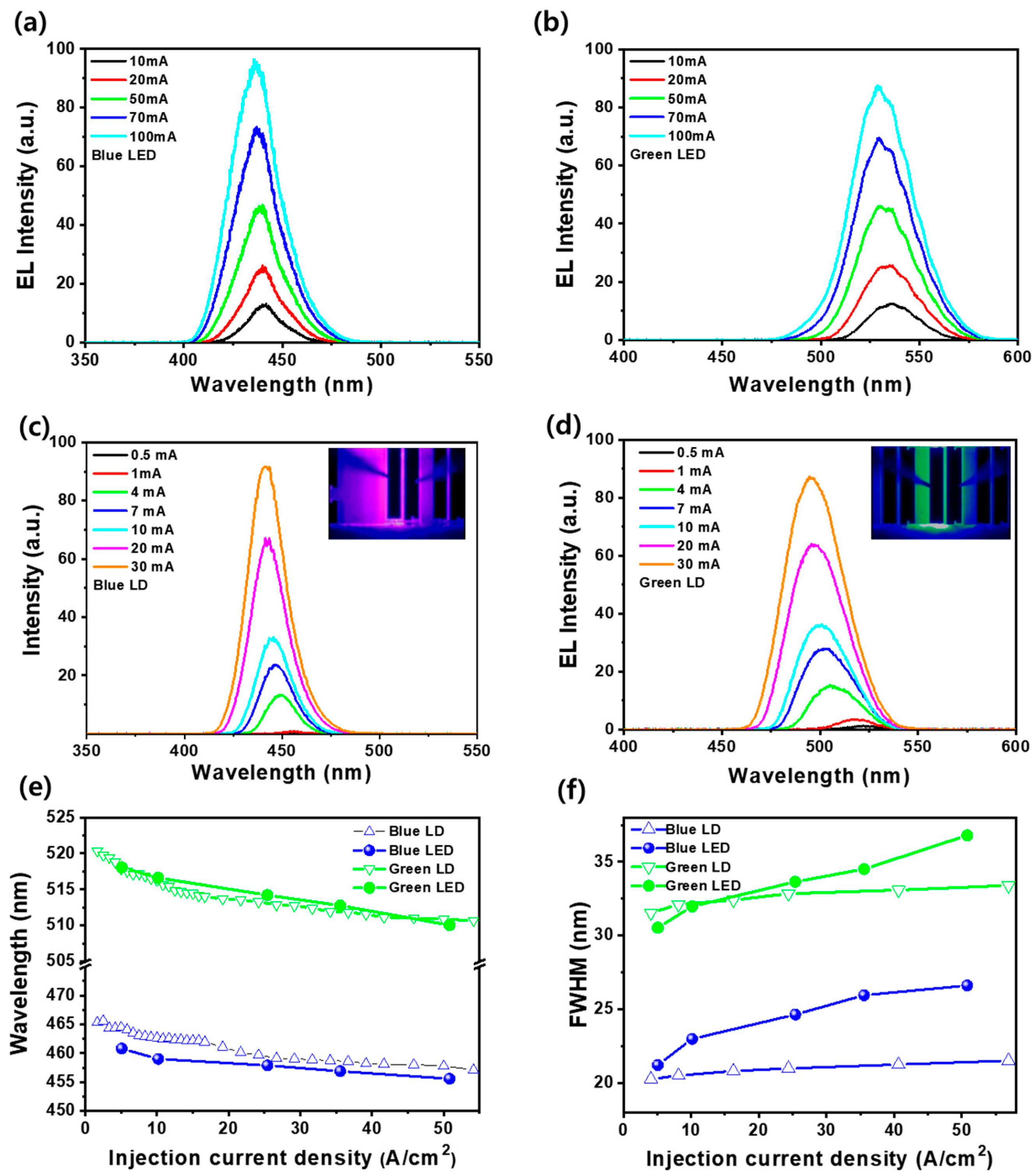
Figure 2a,b show the EL spectra of blue and green LEDs as the injection current increases from 10 mA to 100 mA, respectively. As the injection current increases within this range, the emission wavelengths of blue LEDs exhibit a blue shift from 440.7 to 436.6 nm. Similarly, the green LEDs demonstrate a blue shift from 536.6 to 529.4 nm. The magnitude of the blue shift in a blue LED, at 4.1 nm, is smaller than the 7.2 nm blue shift observed in green LEDs. These shifts can be attributed to the band-filling effect and the strong piezoelectric screening effect [9,18]. In general, differences in miscibility within InN-GaN systems result in more pronounced indium segregation-induced deep localization states in green InGaN QWs structures with a higher indium content compared to blue InGaN QWs. This difference results in a greater blueshift in green LEDs. The blueshift phenomenon due to the band-filling effect occurs as localized energy levels from lower to higher energies fill and recombine as the current injection increases and is particularly pronounced in green InGaN QWs with high indium content [8,9]. Furthermore, it is known that, in GaN films, a pronounced piezoelectric polarization field is observed along the c-axis. Consequently, an increase in the injected current in GaN-based LEDs induces a piezoelectric screening effect within the QWs structures. This effect acts to flatten the inclined bandgap in these structures, thereby leading to a blue shift phenomenon. [9]. In blue and green LDs, similar blueshift phenomena are observed with increasing injection current, as shown in Figure 2c,d. However, there are noticeable differences. For blue LDs, as the injection current increases from 0.5 to 30 mA, a smaller blue shift is observed, moving from 455.6 nm to 441.6 nm. In contrast, green LDs exhibit a more substantial blue shift, ranging from 518.1 nm to 495.9 nm. The greater blue shift in green InGaN QWs is likely due to higher indium composition fluctuations, which may be associated with the band-filling effect or a more significant piezoelectric polarization screen effect compared to blue InGaN QWs [4,19]. In particular, the larger blue shifts in both blue and green LDs can be attributed to the higher injection current densities in LDs compared to LEDs. This is a result of the LDs using a very small region in ridge-type LD structures with dimensions of 2.0 × 650 μm², as opposed to the larger conventional mesa-type LEDs with dimensions of 600 × 600 μm². However, when evaluating the blue shifts of LEDs and LDs based on injection current density, as depicted in Figure 2e, both device types exhibit similar blue shift phenomena. This suggests that, irrespective of the device types, the blue shifts in both are similarly influenced by the injection carrier density, a consequence of shared band-filling and piezoelectric screening effects [9]. However, as depicted in Figure 2e, the emission wavelength of the blue LED is marginally shorter than that of the blue LD, while the emission wavelength of the green LED is comparable to, or slightly longer than, the green LD. This phenomenon can be explained by considering the size and indium localization within the InGaN active regions of these devices. The blue and green LEDs, with a size of 600 μm × 600 μm, are significantly larger—270 times wider—than the LDs, which measure 2.0 μm × 650 μm. This size difference implies that the InGaN active region in the LED has a much higher concentration of indium localized regions compared to that in the LD. Assuming the indium localization per unit area remains constant, the blue LED would have considerably more indium localization states than the blue LD. Despite having the same injection current density, this contributes to a more pronounced blueshift in the blue LED compared to the blue LD. However, as demonstrated in Figure 3, since green InGaN QWs inherently possess much more indium localization states than blue InGaN QWs, it is believed that the emission area does not significantly affect the green LED/LD as much as it does the blue LED/LD. On the other hand, despite the lower turn-on voltage of green LED/LDs compared to blue LED/LDs, owing to the lower energy bandgap in green InGaN LED/LDs, the operation voltage of a green LED is considerably higher than that of a blue LED. However, the operation voltage of a green LD is slightly lower than a blue LD. This discrepancy could be attributed to the inferior electrical properties of the p-type layer grown on relatively poor green InGaN QWs compared to the blue ones, resulting in the higher operation voltage of green LEDs. This implies that the emission energy of green LED may be compromised due to device heating issues arising from the higher operation voltage compared to blue LED. Since heat dissipation is more efficient in LD structures than in LEDs because the heat generated by the active layer is better dissipated into the air due to the narrow 2.0 μm ridge structure, it is believed that green LDs exhibit a slightly lower operating voltage than blue LDs, as shown in Figure 4d. This suggests that, despite the green LD exhibiting relatively high resistance due to the poor characteristics of the p-layer, it displays lower values compared to the blue LD up to an injection current of 20 mA. This is likely due to the formation of a lower turn-on voltage, influenced by the lower bandgap of the green InGaN active layer. Consequently, it is hypothesized that the wavelength of the green LD is either the same or slightly longer than that of the green LED. Nevertheless, despite the potential influence of in-wafer uniformity on the observed wavelength difference, it is crucial to highlight that both blue and green LEDs/LDs undergo a comparable blue shift as the current density increases, unlike the overall injection current. In addition, the EL FWHMs for blue and green LEDs initially show similar trends at low injection current levels below 10 A/cm2, as illustrated in Figure 2f. However, as the injection current density increases, the EL FHWMs of blue and green LEDs gradually increase, while the FWHMs of blue and green LDs experience only a slight increase with injection current density. This difference is likely due to the larger InGaN active region in LEDs compared to LDs, resulting in significantly higher indium localization states for blue and green LEDs. Based on these results, we surmise that the slightly different emission wavelength behaviors of blue and green devices are observed in Figure 2e.
Figure 3a,b present cross-sectional transmission electron microscopy (TEM) images of the InGaN QW regions in both blue and green LED/LD structures. Typically, compared to the growth temperature of GaN film, the growth temperature of InGaN film decreases due to the volatile properties of indium during the growth of InGaN QWs. This reduction in growth temperature aims to increase the indium composition in InGaN QWs, contributing to optical deterioration by inducing indium segregation and crystal defects. In Figure 3a,b, the blue InGaN QWs display a distinct interface between the InGaN well and InGaN barrier, while the green InGaN QWs show a rough interface between the well and barrier. Furthermore, the blue InGaN QWs do not show significant regions of high indium content in the well, whereas the green InGaN QWs exhibit irregular high indium composition areas. This observation suggests that green InGaN QWs experience higher indium composition fluctuations, potentially leading to a high blueshift phenomena due to the band-filling effect, consistent with the blueshifted wavelength and FWHM results shown in Figure 2e,f.
Figure 4a,b show the EL emission intensity of blue and green LEDs and LDs with increasing current injection, respectively. Despite the blue and green LED/LDs sharing nearly identical epitaxial structures, with the primary difference being the indium composition within InGaN QWs, it was observed that the EL intensities of blue LEDs and LDs were approximately 2.5 times higher than those of green LEDs and LDs. This observation suggests that the optical properties of blue InGaN QWs are superior to green InGaN QWs. In general, higher indium content in InGaN QWs leads to an increase in indium localization states, exacerbated by the miscibility gap in the InN-GaN system [9,20]. This results in more crystal defects, which act as nonradiative recombination centers, especially in InGaN QWs with higher indium content. Consequently, it can be inferred that the EL intensities of blue LEDs/LDs are notably superior to those of green LEDs/LDs. However, it is noteworthy that the EL intensities of blue and green LEDs exhibit nearly linear growth with increasing injection current density, whereas the EL intensities of blue and green LDs do not follow a linear increase, as depicted in Figure 4a,b. This is likely due to the much smaller emitting area of the LD compared to the LED under the same injected current, resulting in higher current density and, consequently, diminished efficiency of the LDs. Higher current levels in LDs increase the presence of non-radiative recombination centers, such as Shockley–Read recombination and Auger recombination, leading to a non-linear EL intensity increase that becomes less pronounced with increasing current [12,14]. In terms of operational voltage, green LEDs were observed to have a lower threshold voltage, but a higher operation voltage compared to blue LEDs. The lower threshold voltage in green LEDs correlates with the lower diffusion voltage and energy bandgap compared to blue LEDs. However, the series resistance in green LEDs is higher than that in blue LEDs, leading to a higher operation voltage. This elevated operation voltage is due to the degradation of the p-type layer, grown on a high indium-contained InGaN active region, which can introduce crystal defects into the p-type layer [21,22]. Furthermore, as the band offset between the InGaN well and GaN barrier increases with a rise in indium composition, carrier transport across the InGaN/GaN QWs structure becomes more challenging, resulting in a higher operation voltage for green LEDs. In contrast, the operation voltage of green LDs is slightly lower than that of blue LDs. However, green LDs exhibit significantly higher forward and reverse leakage currents than blue LDs due to the more pronounced crystal defects in green LDs with high indium composition [23,24]. The difference is attributed to the smaller p-type region in LDs, reducing the impact of series resistance from the p-type layer. Consequently, the operation voltage of green LDs aligns more closely with that of blue LDs. However, since the green LD epitaxial layers feature a less robust InGaN active layer and p-type layer, defects are more prone to occur during the ridge dry-etching process, leading to an increase in parallel resistance. This effect ultimately results in higher forward and reverse leakage currents in green LDs when compared to their blue LDs.
Figure 5a illustrates the normalized EQE of blue and green LED/LDs as a function of injection current. The currents at which the maximum EQE is achieved differ between the two, with blue LEDs reaching their peak EQE at 10 mA and green LEDs at 3.0 mA. In the case of blue and green LDs, the maximum EQE is attained at even lower currents, respectively, 1.0 mA for blue LDs and 0.13 mA for green LDs. This variation indicates that green devices, particularly LDs, achieve maximum EQE at lower currents and are more susceptible to efficiency decline at these levels. This phenomenon is attributed to the increase in crystal defects resulting from the agglomeration of indium in the InGaN active layer as indium incorporation into the InGaN active layer increases [8,25]. Furthermore, a decrease in crystallinity in the growing p-type layer leads to an increase in non-radiative recombination centers. In particular, LDs, which have a smaller emission area, exhibit lower currents that yield a higher maximum EQE compared to LEDs, likely due to increased current density in the smaller LDs. At 25 mA, the EQEs are 91.9% for blue LED, 78.8% for green LED, 44.7% for blue LD, and 23.6% for green LD. Similar to the current at which the maximum EQE is achieved, the blue LED maintains a high EQE more effectively than green LEDs, which show more pronounced efficiency degradation due to higher indium content. Despite having the same thin-film structures as LEDs, except for the device structure, both blue and green LDs exhibit efficiency degradation due to the injection of more current into the smaller device area. Figure 5b compares the efficiency degradation of EQE under equivalent current densities for blue/green LED and LD structures. The efficiency droops for blue and green LEDs are 30% and 48% at 50 A/cm2, respectively. However, at this injection current density, blue LDs show a very small EQE droop, while green LDs exhibit a 24.1% droop. This implies that blue LED/LDs exhibit a lower efficiency droop than the green LED/LDs across all the injection current density ranges. Green LED/LDs attain their maximum EQE values at lower injection current densities but suffer from higher efficiency droop than blue LED/LDs. This suggests that the optical properties of blue InGaN QWs outperform those of green InGaN QWs, potentially due to material degradation, such as indium phase separations, as shown in Figure 3a,b. Despite similar epitaxial structures and injection current densities, blue and green LEDs exhibit a higher efficiency droop than blue and green LDs. Since the epitaxial structure and injection current density are identical for LED/LDs, auger recombination and crystal defects can be ruled out as the cause of the efficiency degradation. Therefore, it can be concluded that different device shapes and sizes, such as mesa-type LED and ridge waveguide LD structures, have a more substantial impact on the efficiency degradation of LEDs than LDs. Interestingly, although mesa-structured LEDs have a larger ratio of etched surface area to total device area compared to ridge-type LDs, LDs experience less efficiency degradation at the same injection current density, indicating that surface defect generation during dry etching may not be the direct cause of efficiency degradation. In general, it has been believed that the light extraction efficiency (LEE) of small micro-LEDs below 12 μm can be significantly enhanced by sidewall extraction due to the presence of internal reflection or resonant cavity modes [2,26]. Therefore, the lower efficiency droop characteristics of the LD compared to LED are believed to be due to the LEE enhancement of the 2.0 μm ridge structure.
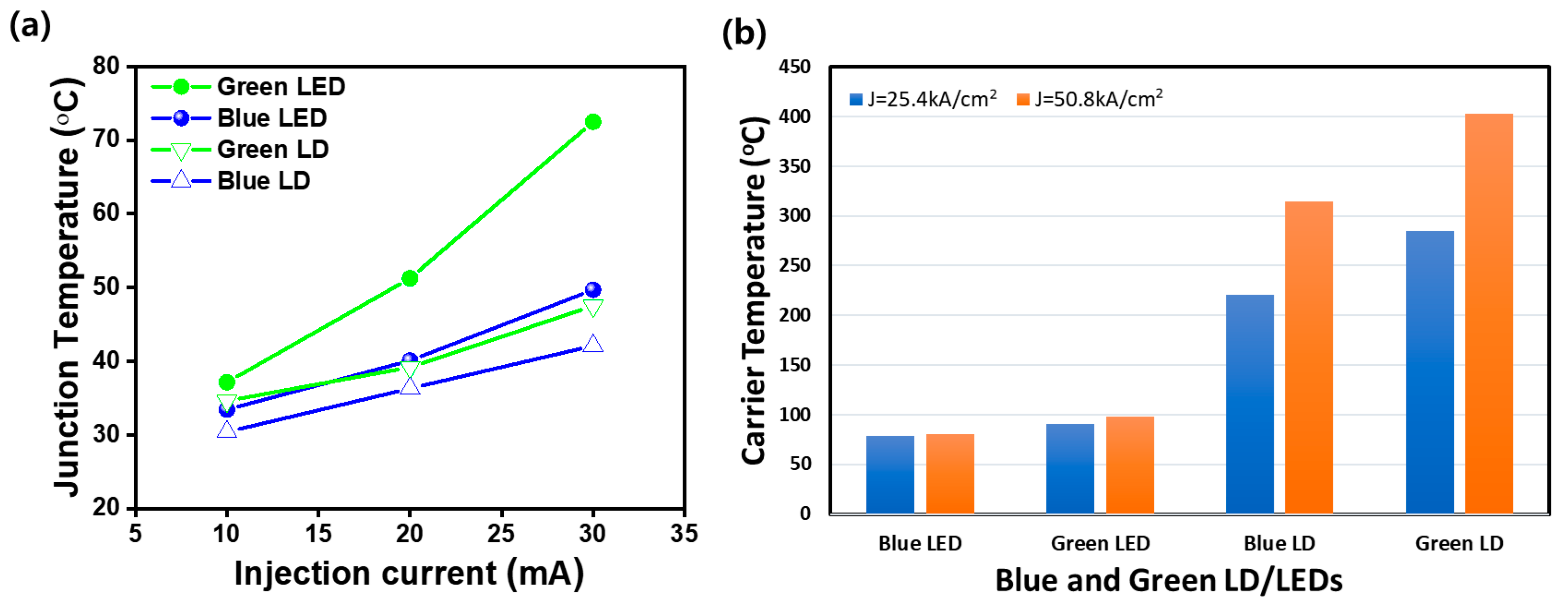
To further clarify the lower efficiency droop of LD, we measured the junction temperatures and carrier temperatures of blue and green LED/LDs [17]. As the injection current was increased from 10 mA to 30 mA, the junction temperature of the blue LED increased from 33.4 °C to 49.7 °C, whereas the junction temperature of the green LED significantly increased from 37.1 °C to 72.5 °C, as shown in Figure 6a. It was observed that the junction temperature of both LED types escalated with the increasing injection current; however, the increase was more pronounced in the green LED than in the blue LED. This greater increase in temperature in the green LED is attributed to the increase in non-radiative recombination due to decreased crystallinity. This reduction in crystallinity stems from the lower growth temperature required for the incorporation of indium in the green InGaN active layer. Furthermore, as the injection current was increased from 10 mA to 30 mA, the junction temperature of the ridge-type blue LDs increased from 30.4 °C to 42.1 °C, and that of the green LDs increased from 34.6 °C to 47.5 °C. Although both blue and green LEDs exhibit a similar pattern of temperature increase, the temperature rise was found to be less significant for LDs compared to LEDs. The lower junction temperatures in LDs compared to LEDs, despite LDs operating at higher current densities compared to LEDs, are likely attributed to differences in their designs. LEDs have a larger area of 600 μm × 600 μm, making it challenging for internally generated heat to dissipate to the outside. On the other hand, LDs utilize very thin ridged structures (2 μm × 650 μm wide), effectively dissipating the heat generated by the active and p-layers outside the thin ridge. Additionally, it was observed that the carrier temperature (Tc) of blue LED/LDs was lower than that of green LED/LDs. This finding is consistent with the junction temperature trends seen in blue and green LDs, and is attributed to the higher presence of non-radiative recombination centers in the green InGaN QWs. Notably, the Tc for both blue and green LDs was significantly lower than that of the blue and green LEDs, respectively. Despite the more pronounced alloy broadening effect in green LDs due to indium fluctuations in the InGaN active layer under identical epitaxial structure for blue and green LDs, the carrier temperature (determined by dI/dE ≈ 1/kTc, where k is the Boltzmann constant, I is EL intensity and E is the photon energy) extracted from the high-energy slope of EL spectra is lower in the LDs than in the LEDs [17]. This is likely because LEDs, having a larger emission area, exhibit a larger FWHM of the EL emission spectrum compared to LDs, as shown in Figure 2. Similar to the junction temperature, the lower Tc of LDs can be attributed to the enhanced heat dissipation capability of the 2 μm × 650 μm ridge waveguide LD structure compared to the 600 μm × 600 μm mesa LED structure, as shown in Figure 6b. Therefore, we suggest that the LD structure is more effective in dissipating heat from the active layer than the LED structure, resulting in a narrower EL FWHM and a lower efficiency droop in the LD structure.
4. Conclusions
We investigated the efficiency droop phenomena in blue and green GaN-based LEDs and LDs, focusing on the spontaneous emission region. Utilizing identical epitaxial structures with only indium composition variations, we conducted experiments across low and very-high injection current regions to exclude proposed causes like electron overflow and crystal defects. The results highlighted that LDs consistently exhibited lower junction and carrier temperatures than LEDs, despite operating at higher current densities. The ridge waveguide LD structure showcased superior heat dissipation, resulting in a narrower emission spectrum and lower efficiency droop compared to mesa LED structures. This underscores the efficacy of LD structure in dissipating heat from the active layer, offering valuable insights for the design optimization of high-power light-emitting devices. The findings contribute to the ongoing efforts to address efficiency droop challenges and enhance the performance of InGaN-based optoelectronic devices.
Author Contributions
Conceptualization, S.-N.L.; methodology, D.-C.C. and Y.S.K.; validation, Y.S.K. and K.-B.K.; resources, S.-N.L.; data curation, D.-C.C. and K.-B.K.; writing—original draft preparation, D.-C.C. and S.-N.L.; writing—review and editing, S.-N.L.; visualization, D.-C.C.; supervision, S.-N.L.; project administration, S.-N.L.; funding acquisition, S.-N.L. All authors have read and agreed to the published version of the manuscript.
Funding
This work was supported by a Research Program (NRF-2020R1A2C1009630) through the National Research Foundation (NRF) of Korea funded by the Ministry of Education, Science and Technology, Republic of Korea.
Institutional Review Board Statement
Not applicable.
Informed Consent Statement
Not applicable.
Data Availability Statement
Data are contained within the article.
Conflicts of Interest
The authors declare no conflicts of interest.
References
- Jia, H.; Guo, L.; Wang, W.; Chen, H. Recent Progress in GaN-based Light-emitting diodes. Adv. Mat. 2009, 21, 4641. [Google Scholar] [CrossRef]
- Lee, G.W.; Oh, J.H.; Lee, S.N. Pulse-modulation controllable monolithic full-color semipolar GaN-based light emitting diodes. Adv. Opt. Mater. 2023, 11, 2301472. [Google Scholar] [CrossRef]
- Lee, S.N.; Cho, S.Y.; Ryu, H.Y.; Son, J.K.; Paek, H.S.; Sakong, T.; Jang, T.; Choi, K.K.; Ha, K.H.; Yang, M.H.; et al. High-power GaN-based blue-violet laser diodes with AlGaN/GaN multiquantum barriers. Appl. Phys. Lett. 2006, 88, 111101. [Google Scholar] [CrossRef]
- Miyoshi, T.; Masui, S.; Okada, T.; Yanamoto, T.; Kozaki, T.; Nagahama, S.; Mukai, T. 510–515 nm InGaN-based green laser diode on c-plane GaN substrate. Appl. Phys. Exp. 2009, 2, 062201. [Google Scholar] [CrossRef]
- Mitchell, B.; Dierolf, V.; Gregorkiewicz, T.; Fujiwara, Y. Perspective: Toward efficient GaN-based red light-emitting diodes using europium doping. J. Appl. Phys. 2018, 123, 160901. [Google Scholar] [CrossRef]
- Hwang, J.I.; Hashimoto, R.; Saito, S.; Nunoue, S. Development of InGaN-based red LED grown on (0001) polar surface. Appl. Phys. Exp. 2014, 7, 071003. [Google Scholar] [CrossRef]
- Hernandez-Cutierrez, C.A.; Kudriavtsev, Y.; Cardona, D.; Cuillen-Cervantes, A.; Santana-Rodriguez, G.; Escobosa, A.; Hernandez-Hernandez, L.A.; Lopez-Lopez, M. InxGa1-x nucleation by In+ ion implantation into GaN. Nucl. Instrum. Methods Phys. Res. B 2017, 413, 62. [Google Scholar] [CrossRef]
- Singh, R.; Doppalapudi, D.; Moustakas, T.D.; Romano, L.T. Phase separation in InGaN thick films and formation of InGaN/GaN double heterostructure in the entire alloy composition. Appl. Phys. Lett. 1997, 70, 1089. [Google Scholar] [CrossRef]
- Chichibu, S.F.; Abare, A.C.; Minsky, M.S.; Keller, S.; Fleischer, S.B.; Bowers, J.E.; Hu, E.; Mishra, U.K.; Coldren, L.A.; DenBaars, S.P.; et al. Effective band gap inhomogeneity and piezoelectric field in InGaN/GaN multiquantum well structures. Appl. Phys. Lett. 1998, 73, 2006. [Google Scholar] [CrossRef]
- Lee, Y.J.; Chen, C.H.; Lee, C.J. Reduction in the efficiency-droop effect of InGaN green light emitting diodes using gradual quantum wells. IEEE Photon. Tech. Lett. 2010, 22, 1506. [Google Scholar] [CrossRef]
- Meng, X.M.; Wang, L.; Hao, Z.; Luo, Y.; Sun, C.; Han, Y.; Xiong, B.; Wang, J.; Li, H. Study on efficiency droop in InGaN/GaN light-emitting diodes based on differential carrier lifetime analysis. Appl. Phys. Lett. 2016, 108, 013501. [Google Scholar] [CrossRef]
- Cho, J.; Schubert, E.F.; Kim, J.K. Efficiency droop in light-emitting diodes: Challenges and countermeasures. Laser Photonics Rev. 2013, 7, 408. [Google Scholar] [CrossRef]
- Bochkareva, N.I.; Rebane, Y.T.; Shreter, Y.G. Efficiency droop in GaN LEDs at high current densities: Tunneling leakage currents and incomplete lateral carrier localization in InGaN/GaN quantum wells. Semiconductor 2014, 48, 1079. [Google Scholar] [CrossRef]
- Kim, M.H.; Schubert, M.F.; Dai, Q.; Kim, J.K.; Schubert, E.F.; Piprek, J.; Park, Y. Origin of efficiency droop in GaN-based light-emitting diode. Appl. Phys. Lett. 2007, 91, 183507. [Google Scholar] [CrossRef]
- Zheleva, T.S.; Smith, S.A.; Thomson, D.B.; Linthicum, K.J.; Rajagopal, P.; Davis, R.F. Pendeo-epitaxy: A new approach for lateral growth of gallium nitride films. J. Electron. Mat. 1999, 28, L5. [Google Scholar] [CrossRef]
- Oh, J.H.; Baek, S.H.; Shin, S.U.; Min, K.T.; Lee, S.N. High-efficiency flat-type nitride-based micro-light emitting diodes using local breakdown conductive channel. J. Alloys Compd. 2023, 956, 170239. [Google Scholar] [CrossRef]
- Schubert, E.F. Light-Emitting Diodes, 2nd ed.; Cambridge University Press: New York, NY, USA, 2006; p. 101. [Google Scholar]
- Wang, L.; Lu, C.; Lu, J.; Liu, L.; Liu, N.; Chen, Y.; Zhang, Y.; Gu, E.; Hu, X. Influence of carrier screening and band filling effect on efficiency droop of InGaN light emitting diodes. Opt. Exp. 2011, 19, 14182. [Google Scholar] [CrossRef] [PubMed]
- Baek, S.H.; Kim, H.W.; Lee, G.W.; Lee, S.N. Monolithic multi-color tunable inorganic light-emitting diodes. Adv. Electon. Mater. 2022, 8, 2100598. [Google Scholar] [CrossRef]
- Cho, H.K.; Lee, J.Y.; Song, J.H.; Yu, P.W.; Yang, G.M.; Kim, C.S. Influence of strain-induced indium clustering on characteristics of InGaN/GaN multiple quantum wells with high indium composition. J. Appl. Phys. 2002, 91, 1104. [Google Scholar] [CrossRef]
- Meneghini, M.; Rigutti, L.; Trevisanello, L.R.; Cavallini, A.; Meneghesso, G.; Zanoni, E. A model for the thermal degradation of metal/(p-GaN) interface in GaN-based light-emitting diodes. J. Appl. Phys. 2008, 103, 063703. [Google Scholar] [CrossRef]
- Lee, W.; Limb, J.; Ryou, J.H.; Yoo, D.; Chung, T.; Dupuis, R.D. Influence of growth temperature and growth rate of p-GaN layers on the characteristics of green light emitting diodes. J. Electron. Mat. 2006, 35, 587. [Google Scholar] [CrossRef]
- Zhi, T.; Tao, T.; Liu, B.; Chen, P.; Zhang, R. Reverse leakage current characteristics of GaN/InGaN multiple quantum-wells blue and green light-emitting diodes. IEEE Photonics J. 2016, 8, 1. [Google Scholar] [CrossRef]
- Zhou, S.; Lv, J.; Wu, Y.; Zhang, Y.; Zheng, C.; Liu, S. Reverse leakage current characteristics of InGaN/GaN multiple quantum well violet/blue/green light-emitting diodes. Jpn. J. Appl. Phys. 2018, 57, 051003. [Google Scholar] [CrossRef]
- Bazioti, C.; Papadomanolaki, E.; Kehagias, T.; Walther, T.; Smalc-Koziorowska, J.; Pavlidou, E.; Komninou, P.; Karakostas, T.; Iliopoulos, E.; Dimitrakopulos, G.P. Defects, strain relaxation, and compositional grading in high indium content InGaN epilayers grown by molecular beam epitaxy. J. Appl. Phys. 2015, 118, 155301. [Google Scholar] [CrossRef]
- Choi, H.W.; Jeon, C.W.; Dawson, M.D.; Edwards, P.R.; Martin, R.W.; Tripathy, S. Mechanism of enhanced light output efficiency in InGaN-based microlight emitting diodes. J. Appl. Phys. 2003, 93, 5978. [Google Scholar] [CrossRef]
Figure 1.
(a) Maskless laterally epitaxial overgrowth procedures of GaN film to reduce the crystal defect, (b) the cross-sectional transmittance electron microscopic image of GaN-based LD structure growth on maskless LEO-GaN template, the schematic diagram of (c) conventional mesa-type LED, and (d) ridge-type LD structures.

Figure 2.
The EL spectra of InGaN-based (a) blue LED, (b) green LD, (c) blue LD, and (d) green LD. The EL (e) emission wavelength and (f) spectral FWHM of blue LED/LD and green LED/LD as a function of injection current density.
Figure 2.
The EL spectra of InGaN-based (a) blue LED, (b) green LD, (c) blue LD, and (d) green LD. The EL (e) emission wavelength and (f) spectral FWHM of blue LED/LD and green LED/LD as a function of injection current density.

Figure 3.
High resolution TEM images of (a) blue and (b) green InGaN QWs regions in light-emitting device structures.
Figure 3.
High resolution TEM images of (a) blue and (b) green InGaN QWs regions in light-emitting device structures.

Figure 4.
Current (I)-light output power (L) curves of blue and green (a) LEDs and (b) LDs. Log (I)-voltage (V) curves of blue and green (c) LEDs and (d) LDs. Insets of (c) and (d) linear I-V curves of blue and green LEDs and LDs, respectively.
Figure 4.
Current (I)-light output power (L) curves of blue and green (a) LEDs and (b) LDs. Log (I)-voltage (V) curves of blue and green (c) LEDs and (d) LDs. Insets of (c) and (d) linear I-V curves of blue and green LEDs and LDs, respectively.

Figure 5.
Normalized external quantum efficiency of blue and green LED/LDs as a function of (a) injection current and (b) injection current density.
Figure 5.
Normalized external quantum efficiency of blue and green LED/LDs as a function of (a) injection current and (b) injection current density.

Figure 6.
Junction temperatures (a) and carrier temperatures (b) of blue/green LEDs and LDs with different injection current and current densities.
Figure 6.
Junction temperatures (a) and carrier temperatures (b) of blue/green LEDs and LDs with different injection current and current densities.

Disclaimer/Publisher’s Note: The statements, opinions and data contained in all publications are solely those of the individual author(s) and contributor(s) and not of MDPI and/or the editor(s). MDPI and/or the editor(s) disclaim responsibility for any injury to people or property resulting from any ideas, methods, instructions or products referred to in the content. |
© 2024 by the authors. Licensee MDPI, Basel, Switzerland. This article is an open access article distributed under the terms and conditions of the Creative Commons Attribution (CC BY) license (https://creativecommons.org/licenses/by/4.0/).
Share and Cite
MDPI and ACS Style
Choi, D.-C.; Kim, Y.S.; Kim, K.-B.; Lee, S.-N. Spontaneous Emission Studies for Blue and Green InGaN-Based Light-Emitting Diodes and Laser Diodes. Photonics 2024, 11, 135. https://0-doi-org.brum.beds.ac.uk/10.3390/photonics11020135
AMA Style
Choi D-C, Kim YS, Kim K-B, Lee S-N. Spontaneous Emission Studies for Blue and Green InGaN-Based Light-Emitting Diodes and Laser Diodes. Photonics. 2024; 11(2):135. https://0-doi-org.brum.beds.ac.uk/10.3390/photonics11020135
Chicago/Turabian StyleChoi, Dae-Choul, Yoon Seok Kim, Kyoung-Bo Kim, and Sung-Nam Lee. 2024. "Spontaneous Emission Studies for Blue and Green InGaN-Based Light-Emitting Diodes and Laser Diodes" Photonics 11, no. 2: 135. https://0-doi-org.brum.beds.ac.uk/10.3390/photonics11020135
Note that from the first issue of 2016, this journal uses article numbers instead of page numbers. See further details here.