An Optical Analog-to-Digital Converter with Enhanced ENOB Based on MMI-Based Phase-Shift Quantization


School of Electronic Engineering, Beijing University of Posts and Telecommunications, Beijing 100876, China
*
Author to whom correspondence should be addressed.
Photonics 2021, 8(2), 52; https://0-doi-org.brum.beds.ac.uk/10.3390/photonics8020052
Submission received: 25 January 2021
/
Revised: 10 February 2021
/
Accepted: 11 February 2021
/
Published: 14 February 2021
(This article belongs to the Special Issue Photonics for Emerging Applications in Communication and Sensing)
Abstract
:An optical analog-to-digital converter (OADC) scheme with enhanced bit resolution by using a multimode interference (MMI) coupler as optical quantization is proposed. The mathematical simulation model was established to verify the feasibility and to investigate the robustness of the scheme. Simulation results show that 20 quantization levels (corresponding to 4.32 of effective number of bits (ENOB)) are realized by using only 6 channels, which indicates that the scheme requires much fewer quantization channels or modulators to realize the same amount of ENOB. The scheme is robust and potential for integration.
1. Introduction
High-speed analog-to-digital converters (ADC) play an important role in modern signal processing, such as high-frequency radar systems [1,2,3,4,5], wireless communications [6,7], and image processing [8,9], etc. However, with more and more wideband applications, such as wireless and radar communications especially when the bandwidth of radar signals is over 10 GHz, traditional electronic ADCs have been unable to meet the requirements of high speed due to timing jitter, thermal noise and uncertainty of electronic components, and so on. In recent years, with the rapid development of photonic technology, using photonic technology to break through the bottleneck of electronic ADC has become a research hotspot in the field of optoelectronic technology [10]. The advantage of using photonic technology in ADC is that the sampling rate can be up to 100GS/s (samples per second) or even higher. Moreover, the timing jitter of the optical pulse can reach the level of femtosecond [11,12], which is two orders of magnitude smaller than that of the electrical sampling pulse. In addition, the pulse width can be compressed to the order of picoseconds or even femtoseconds by using pulse compression technology [13]. Therefore, optical analog-to-digital conversion (OADC) technology has significant advantages compared with traditional electronic ADC technology. In general, OADC has great potential not only in terms of high speed, high precision, and wide bandwidth, etc., but also in commercial applications due to the great development of photonic integration. Thus, it has become one of the main development directions of high-speed ADC.
In last decades, lots of optical-sampling electrical-quantization [14,15] and optical-sampling optical-quantization schemes have been reported, which can be divided into two categories, i.e. intensity-to-wavelength optical quantization and phase-shift optical quantization (PSOQ). Intensity-to-wavelength optical quantization [16,17] usually realizes intensity to wavelength conversion by using nonlinear effects via nonlinear devices, like highly nonlinear fiber (HNLF). However, the length of HNLF is usually up to km level and the optical power required is relatively large to excite the nonlinear effect. On the other hand, the PSOQ scheme, which was firstly proposed by Taylor [18] and then developed in [19,20,21,22,23], typically uses electro-optic modulators with multiplied half-wave voltages. The advantages of Taylor’s and its developed schemes are potentiality of on-chip integration and have low requirement of input optical power due to operation principle based on optical interference. In general, in Taylor’s and its developed schemes, optical quantization of N bit requires N modulators. To further increase the quantization bits, the half-wave voltage of the last modulator must be significantly reduced. Therefore, we previously proposed a cascade step-size (CSS) multimode interference (MMI) coupler-based phase quantization scheme [24] requiring only one phase modulator (PM). In the scheme reported in [24], in order to realize N bit, only one phase modulator and a CSS-MMI with 2N-1 output channels are needed. This scheme avoids the increasing requirement of the number of modulators when N increases in the schemes developed from Taylor’s scheme, and eliminates the need for ultra-low half-wave voltage of modulators. However, when N is larger, the number of output channels (K) increases significantly (for example, when N is 4.17 bit, K is 9; whereas N is 5.09 bit, K is 17, and so on), resulting in enormous difficulties in design and fabrication of CSS-MMI.
In this paper, in order to obtain effective number of bits (ENOB) as high as possible in OADC with the required number of modulators and optical output channels as fewer as possible, we propose a new PSOQ scheme of OADC, which effectively increases the number of quantization bits but requires much fewer optical channels and modulators. We numerically demonstrate the scheme with 6 optical channels and 2 modulators by using a 1 × 4 MMI, a 3 × 5 MMI, a PM, and a Mach-Zehnder modulator (MZM), which can achieve 4.32 bit. Compared with our previously proposed scheme [24], which needs 9 optical channels to achieve 4.17 bit, this new scheme is easier for design and fabrication. Moreover, we investigated the performance of the proposed scheme by building up a simulation system, and found that compared with the previous scheme, the proposed scheme not only has much fewer output channels, but also has more robustness in presence of timing jitter, intensity noise of optical sampling pulses, and MMI power imbalance.
2. Principle of Operation
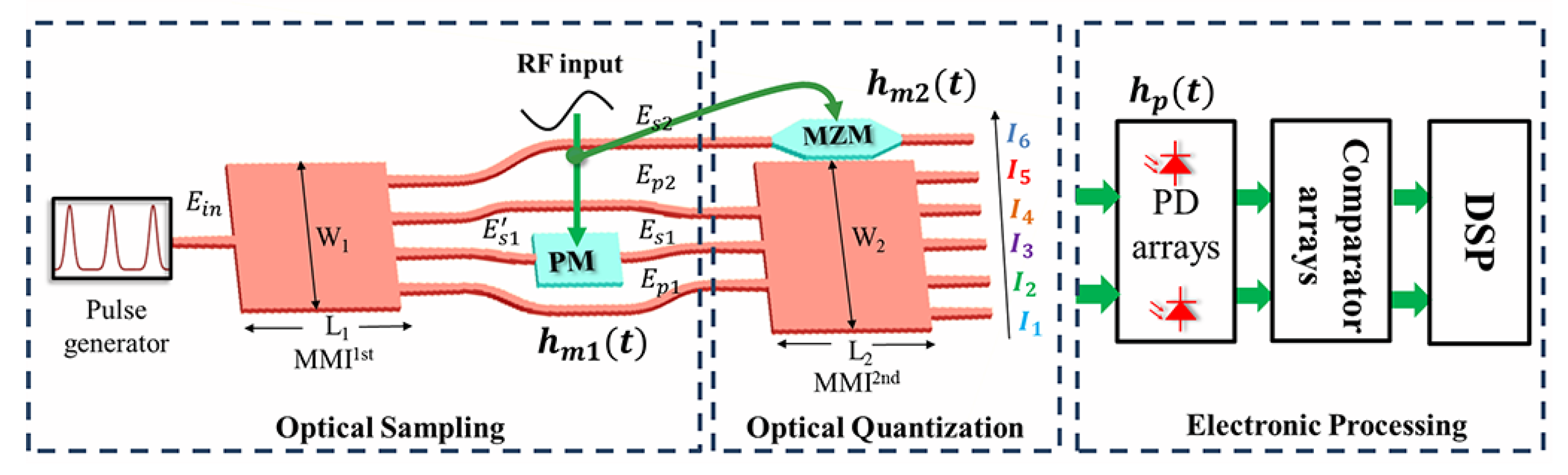
The schematic diagram of the proposed OADC is shown in Figure 1. It consists of an optical sampling module, an optical quantization module, and an electrical back-end processing module. The optical sampling module is composed of a pulse laser, a 1 × 4MMI (MMI1st), and a PM. The optical quantization module is composed of a 3 × 5 MMI (MMI2nd) and an MZM. The digital signal processing module is composed of photo-detector (PD) arrays and electric comparator arrays.
Firstly, in the optical sampling module, assuming that the injected high-speed pulses emitted by the pulse laser are solitary pulses with Gauss shape, can be represented as
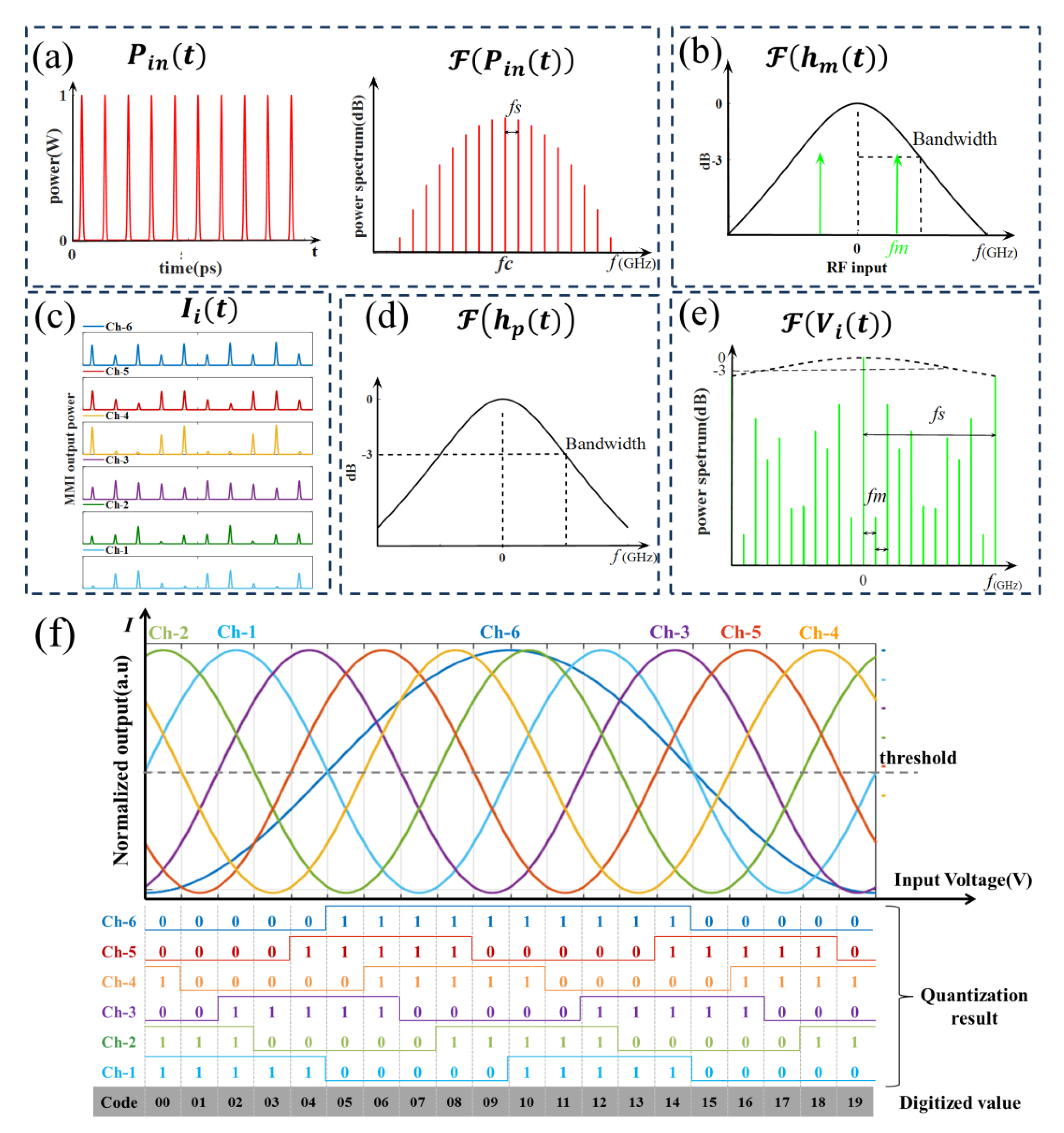
where , () is the sampling rate. is the peak power of the pulse. The full width at half maximum power (FWHM) pulse duration is and m denotes the order of the super-Gaussian function. The carrier frequency of the optical pulse is defined by emission frequency and the initial phase is . Therefore, the schematic of waveforms of the sampling pulses is shown in Figure 2a.
The high-speed pulses are divided into four channels with equal power by MMI1st, the outputs of MMI1st can be described as
After splitting, optical pulse passes through PM which is driven by input signal , and becomes as
where is the equivalent model of a phase modulator which reflects the high frequency characteristics of the phase modulator. The electronic frequency response is shown as Figure 2b, where is the frequency of the RF (Radio-frequency) input. can be equivalent to , where and are the half-wave voltage and bias voltage of PM, respectively. is induced by . Then is injected at the middle position of MMI2nd, while and are injected at positions as
where K is the number of MMI2nd output channels, here K = 5. After carefully choosing the dimensions of MMI2nd, K images of equal intensities can be formed at MMI2nd output. The output power can be expressed as
where . From Equation (5), we can see that the output power of each channel varies sinusoidally with as shown in Figure 2f. This is similar to [24] and acts as quantizer which can realize 10 quantization levels (corresponding to 3.32 bit). The output pulses of each channel are shown in Figure 2c. Based on the principle in [24], in order to extend the ENOB, the 3 × 5 MMI should be replaced by a 3 × 9 MMI, thus OADC can be extended to 18 quantization levels, which means a 4.17 bit OADC with 9 output channels is obtained.
In this paper, we propose a new scheme to extend the ENOB by introducing a MZM. As shown in Figure 1, the MZM with a half-wave voltage of 2 is introduced parallel to the PM, with as input. The output power of MZM can be expressed as
where is the numerical model of MZM and reflects the high frequency characteristics of the MZM. is equivalent to , is the bias voltage applied to MZM.
After the optical-to-electrical (O/E) conversion performed by the PD arrays, we can obtain the electrical signal as
is the noise current caused by PD in each channel, is the equivalent circuit model of PD as shown in Figure 2d and the power spectrum of is Figure 2e. is load resistance that converts current into voltage output.
Next, the detected signals of the 6 output channels are injected into the electric comparator arrays, judged to “0” or “1” by appropriate threshold as
Generally, and . is the threshold voltage of electric comparator arrays, is the minimum identification precision voltage, which is related to the conversion precision of the comparator. The higher the is, the smaller the will be, which shows that the comparator has more accurate comparison results.
At last, after processing these digital signals according to the electronic decision rules as shown in Figure 2f, we can get 20 different quantization levels. We can see from Figure 2f that, the transmission periods of Channel 1 to Channel 5 are . For Channel 1 to Channel 5 we can obtain 10 quantization levels range from 0 to 2, and the encoding is repeated within 2 to 4. Channel 6 is synchronized with other channels, but the transmission period is 4. By combining all 6 channels, 20 quantization levels are obtained in the input voltage ranging from 0 to 4. Compared with our previously proposed scheme (where 18 quantization levels are obtained with 9 output channels), the proposed scheme needs fewer channels (6 channels) to obtain equivalent quantization levels (i.e., ENOB).
3. Simulation Modelling and Performance Analysis
Based on the above models, the OADC is built up to verify the feasibility and investigate the performance of the proposed OADC scheme, as shown in Figure 3. We analyze the OADC performance based on IEEE standard [25], where ENOB is derived as [25]
SINAD (signal-to-noise ratio) well reflects the overall dynamic performance of the ADC because it includes all factors that constitute noises and distortions. Based on IEEE standard, SINAD is calculated from the frequency spectrum of the digital output codes of the ADC as
where is the electrical signal power, and represent inherent quantization errors and errors caused by other noise, respectively.
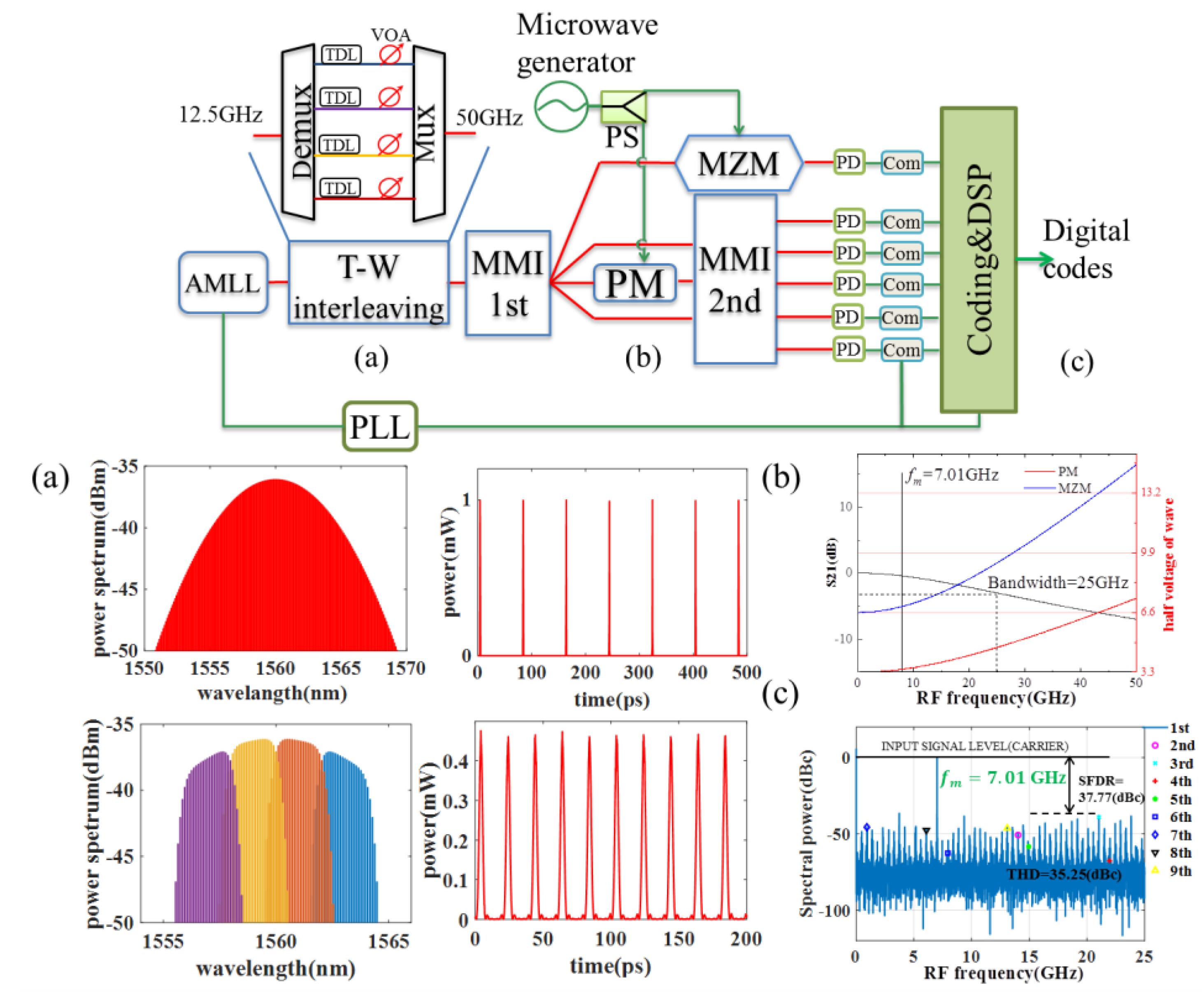
We use time-wavelength interleaving (T-W interleaving) to acquire optical sampling pulses with = 50 GHz. The waveforms of the output of active mode-locked laser (AMLL) is shown in Figure 3a, whereas the time-wavelength interleaved sampling pulses are shown in Figure 3a. A sine wave signal of 7.01 GHz was used to act as an electrical analog signal, which is divided into two by power splitter (PS), one of which is used to drive the PM, while the other one is used to drive the MZM. Based on the principle analysis, the ideal ENOB is 4.32 bit. Then we took imperfections in the actual system into account to calculate the ENOB. Table 1 shows the main simulation parameters of the OADC. The parameters chosen in Table 1 are based on the datasheet of commercially available devices.
For example, the parameters of AMLL was chosen based on the datasheet of Calmar PS-10-TT series, like timing jitter is 100 fs, the standard deviation of random intensity noise (RIN) is 2% relative to the pulse peak power, and the of the Gaussian pulse train is 0.5 ps, peak power is 0 dBm, and wavelength is 1560 nm.
As for modulators, with the increase of input RF frequency, RF and light wave speed mismatch and transmission loss caused by the structural parameters of lithium niobate modulator increase as well, which in turn affects the output optical signal. Therefore, it is important to analyze the performance of OADC under this influence. The RF response of modulator can be represented by S21 response, which decreases with the input frequency increasing. This will affect the OADC output phase and as shown in Figure 3b. In our simulation, the half-wave voltages of PM and MZM were set as 3.3 V@1 GHz and 6.6 V@1 GHz referring to the commercial modulator, and the S21 data of commercial devices were taken into account. MMI transmission curves were obtained according to measurement results based on our fabricated MMI [26], which has normalized channel power imbalance of [0.943 1.010 1.027 0.884 1.136], leading to non-uniform quantization and thus decreasing the ENOB of the OADC.
In the electronic processing module, the parameters of PD were chosen according to the silicon germanium PIN structure photodetector mentioned in [27,28,29], as bandwidth of 40 GHz, a load resistance of 50 Ω, dark current of 5 nA, electronic measurement bandwidth and resistance-related thermal noise, and shot noise related to input optical power. Similarly, the parameters for electrical comparators were set with reference to the offset voltage and minimum conversion accuracy of commercial electrical comparators (ADI, MP582). The electrical components are synchronized with the active mode-locked laser (AMLL) through a phase-locked loop (PLL). The root mean square period jitter (RMS(Jper)) caused by phase noise of PLL internal electronic circuits is set to 63 fs according to commercial PLL (Texas Instruments, LMX2820).
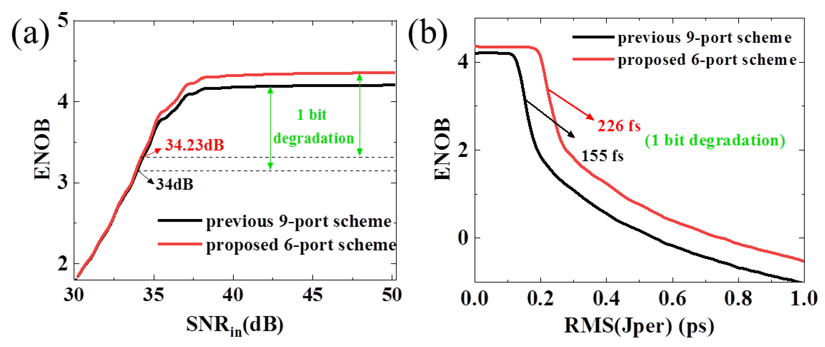
At last, according to the output digital code and , the frequency of the input signal is calculated according to the FFT calculation result and Equation (9) as shown in Figure 3c, which is consistent with the given input signal , verifying the correctness of the simulation modelling, the SINAD is calculated to be 26.03 dB. Therefore, the ENOB is 4.03 bit, which is a little slighter than the ideal ENOB of 4.32 bit and demonstrates the accuracy of the simulation modelling of the proposed OADC scheme.
Table 2 compares the performance of different reported schemes based on PSOQ, “-” in Table 2 means that CW (continuous-wave) light was used or non-mentioned in the schemes. We can see from Table 2 that our proposed scheme has a simpler structure due to the fact that the optical quantizer is a passive device and has fewer optical channels and accepted number of modulators, which is a potential for on-chip integration (similar optical quantizer with 5 channels has already been experimentally reported [26]).
Next, in order to investigate the robustness of the OADC, we investigated the factors that RIN and timing jitter of the pulse source, the MMI channel imbalance and signal noise, phase noise of PLL on ENOB.
3.1. RIN and Timing Jitter
The actual optical sampling pulse has timing jitter, RIN, and limited pulse width. These characteristics of the optical pulse cause errors in sampling process, reduce the SINAD of the OADC, and degrade the ENOB. It is important to investigate the effects of RIN and timing jitter, as both time-wavelength interweaving and back-end electrical processing also lead to mismatches and amplitude fluctuations throughout the OADC. Therefore, we investigated the impact of RIN and timing jitter on ENOB. RIN is defined as , where is intensity noise, and is pulse peak power. Full scale modulation is assumed in the calculation and the amplitude of the RF input is . Therefore, the error caused by RIN can be substituted into Equation (10) to calculate SINAD
Timing jitter can be defined as . The judgment time of the sampling pulse is . According to the power shape is given by , Equation (7), we can calculate the SINAD caused by timing jitter as following
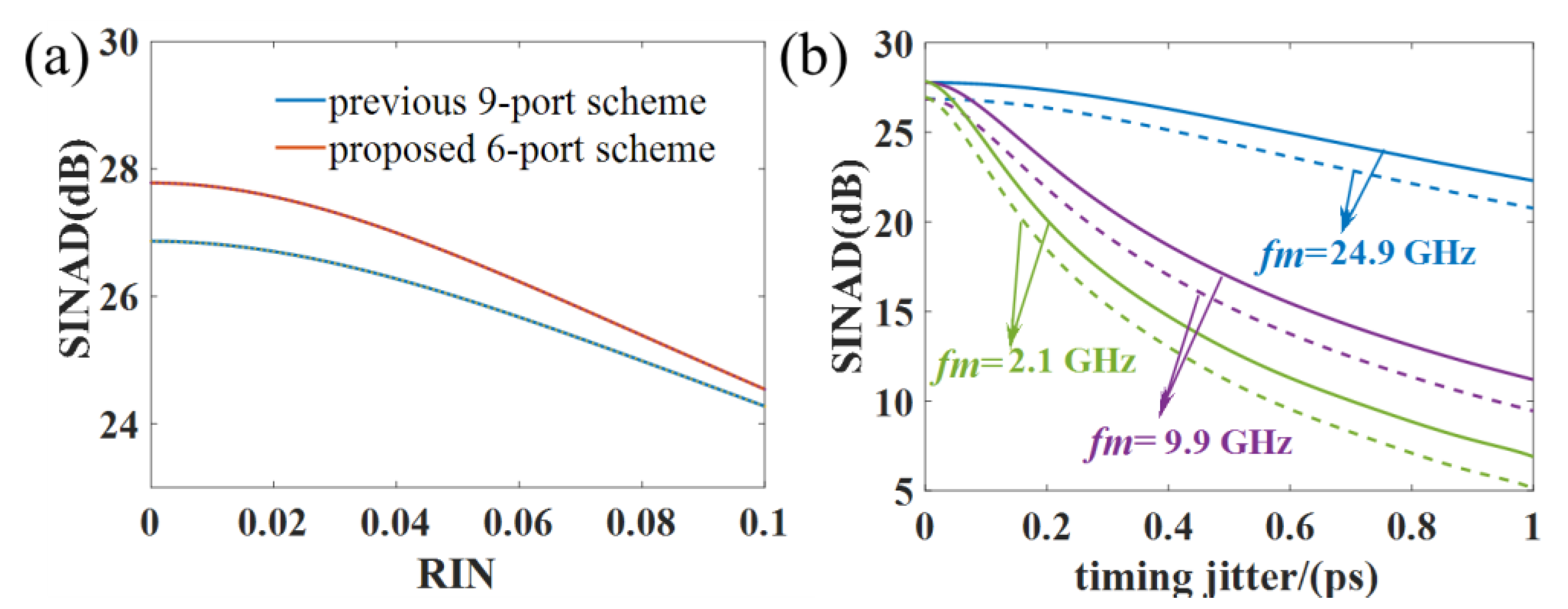
It can be seen from Equation (12) that SINAD is related to and the frequency of the input signal. GHz is set in the calculation. SINAD degrades when RIN increases, which can be theoretically obtained as shown in Figure 4a. As shown in Figure 4b, SINAD drops faster when increases, because there is a greater risk of error in judgment time.
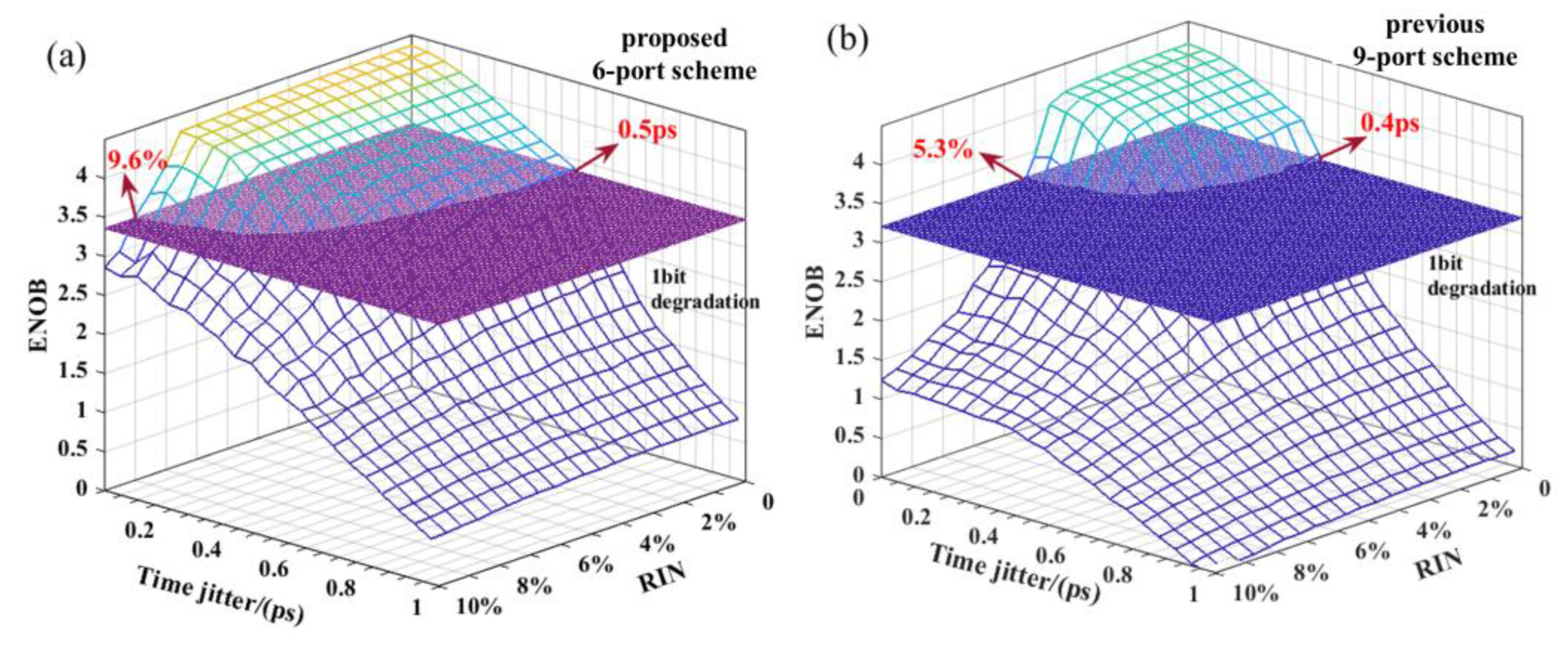
We demonstrate how RIN and timing jitter affect system performance from the mathematical model. We carried out the simulation operation when sample rate of optical pulse is 100 GHz and in our simulation modelling. The final 215 digital codes were selected to calculate FFT and the final ENOB was obtained. Here, equals to −5 dBm, we changed RIN from 0 to 10%, timing jitter from 0 ps to 1 ps. The results of ENOB vs. timing jitter and RIN are shown in Figure 5a as a 3D graph. The same investigation was also carried out for our previously 9-port scheme with equivalent ENOB for comparison. The results of the previous 9-port scheme are shown in Figure 5b. We can see from Figure 5 that ENOB decreases greatly with the increase of RIN and timing jitter. When ENOB degrades by 1 bit, in Figure 5a, RIN tolerance is 9.6%, while in Figure 5b RIN tolerance of our previous 9-port scheme is 5.3%. The results indicate that the new proposed OADC has lower requirements on RIN of the sampling pulses. As for timing jitter, we can see that when ENOB degrades by 1 bit, the tolerance of timing jitter is 0.5 ps, while the previous 9-port scheme is 0.4 ps as shown in Figure 5b. The results indicate that the proposed scheme is more robust to timing jitter.
3.2. Channel Imbalance
Channel equalization refers to the consistency in amplitude of the modulation curve outputs of the quantizer (MMI2nd). The channel imbalance of the MMI2nd may be caused by manufacturing process errors, or design errors. Therefore, it is important to investigate the effect of channel imbalance of MMI2nd on ENOB.
The power imbalance of each channel is expressed by , i = 1…K. Therefore, the SINAD under the error caused by channel imbalance is given by
where i = 1…K. Since the of each channel is different, when calculating the effect of on OADC performance, it can be represented by
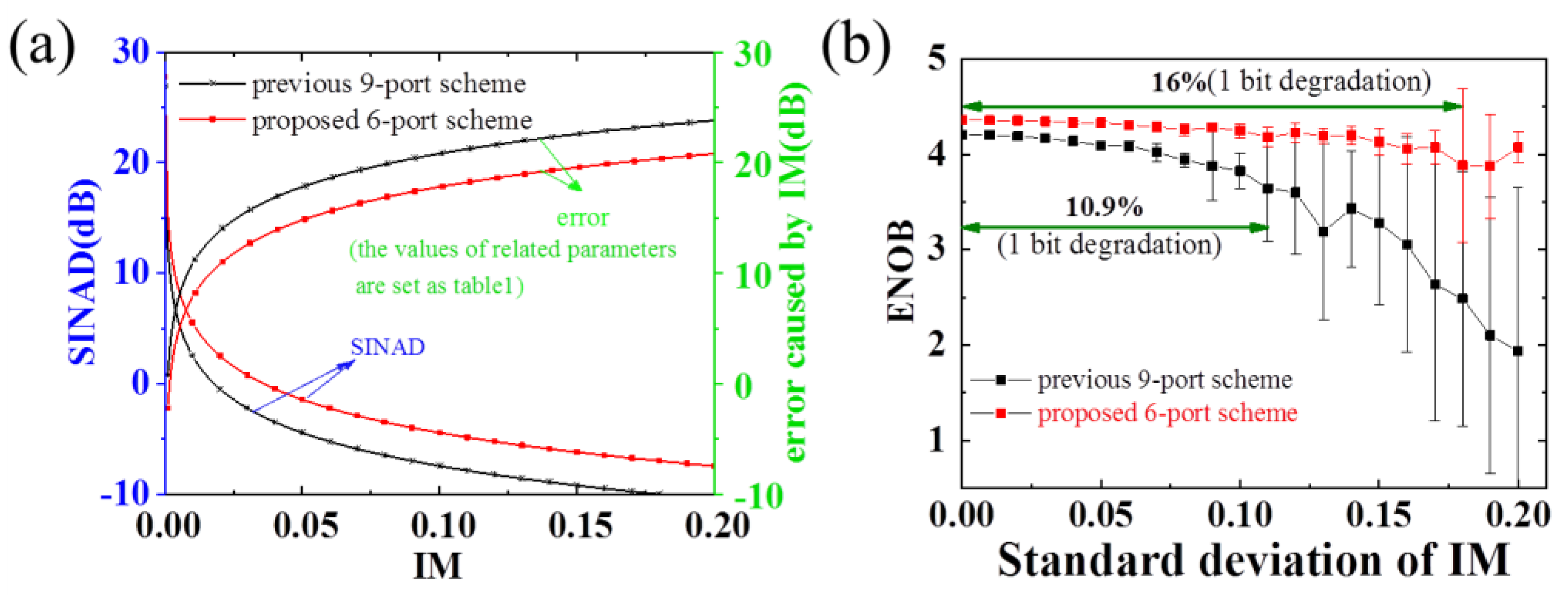
It can be seen from Equation (13) that SINAD is related to the number of channels of MMI2nd. As shown in Figure 6a, SINAD drops faster with more channels, because there is a greater probability of errors in the judgement. Different IM values are set in the simulation to observe the impact on ENOB of the OADC. In simulation, ENOB was calculated by 50 times for the same IM values. The red curve in Figure 6b shows ENOB degradation induced by IM, the results for previous 9-port scheme are shown as a black curve. We can see that both ENOB degrades with IM increasing, this is because due to the imbalance, the actual quantization step size is different from the ideal quantization step size, which would lead to non-uniform quantization errors and make harmonic noise power increase, resulting in a decrease in ENOB. Furthermore, as shown in Figure 6b, it has been verified by 50-time simulations that if the ENOB degrades by 1 bit, the tolerance of IM of the proposed scheme can be 16%, but the previous 9-port scheme has only 10.9% tolerance. In comparison, the proposed scheme is more robust to the power imbalance of the quantizer. We can also see that under the same IM, because the proposed scheme has fewer ports, the probability of error in the output digital code is smaller than that of the previous 9-port scheme.
3.3. Electronic Devices Noise
The noise introduced by the electrical devices in the OADC also affects the performance of the OADC. Here we analyze two typical effects on the ENOB of the OADC. One is the noise of the input analog RF signal, the other is the phase noise of the PLL used to synchronize the sampling pulses with comparators and coding circuits, etc.
3.3.1. The Noise of Input Signal
The signal source and RF amplifier may introduce noise. Therefore, we analyzed the noisy signal on the performance of OADC. The signal to noise ratio (SNR) of the analogue signal is expressed as . Assuming that the noise added to the analogue signal is a Gaussian random signal with a mean value of 0. Therefore, the SINAD under the error caused by noise is given by
where is the power of the noisy signal. It can be seen from Equation (15) that SINAD is related to the quantization level N. We carried out the simulation operation with other parameters unchanged. The results of ENOB vs. are shown in Figure 7a. Dozens of simulations have been carried out to eliminate the contingency of the results, which indicate that the higher the number of quantization levels, the faster the ENOB decreases. That is to say that the noise of the input signal has a greater impact on OADC with bigger ENOB, thus the SNR of the input signal cannot be ignored.
3.3.2. Phase Noise of PLL
The reference clock signal of the PLL is the synchronous output of the pulse laser, thus PLL could provide a locked clock to the electronic comparators and coding circuits. However, the clock signal generated from an actual PLL has phase noise (), which is equivalent to the jitter of the clock signal (, that represents clock non-synchronization. The clock jitter , which is a random disturbance signal and described by root mean square value (RMS) as
where is clock frequency, is the power spectrum of phase noise.
Different RMSs of clock jitter are added in the theoretical calculation and simulation to analyze the influence on OADC. According to , Equation (7), we can calculate the SINAD caused by clock jitter as following
It can be seen from Equation (17) that SINAD drops faster when increases, because there is a greater risk of error in judgment time. We changed RMS() from 0 to 1 ps, and maintained the other parameters. The results of ENOB vs. clock jitter are shown in Figure 7b. When ENOB degrades by 1 bit, RMS() tolerance is 226 fs for the proposed scheme, while it is 155 fs for our previous 9-port scheme. The results indicate that the new proposed OADC has lower requirements on phase noise of PLL due to fewer channels than previous 9-port scheme.
4. Conclusions
In this paper, a new OADC scheme with ENOB enhanced by introducing an MZM to increase the optical quantization levels has been proposed and demonstrated in simulation. Based on the operation principle, 20 quantization levels (corresponding to 4.32 of ENOB) are realized by using only 6 channels, which indicates that the scheme requires much fewer quantization channels or modulators to realize the same amount of ENOB. A numerical analysis and proof-of-concept demonstrations were carried out to verify the feasibility and robustness of the scheme. Simulation results show that 4.03 of ENOB is realized for 7.01 GHz RF signal under 50 GHz sampling rate, which indicates that the proposed scheme requires much fewer quantization output channels or modulators to realize the same amount ENOB, compared with our previous 9-port scheme. We analyzed the influence of RIN and timing jitter of sampling pulses and the channel imbalance of MMI2nd on ENOB of both the proposed OADC scheme and the previous 9-port scheme. The simulation results show that the proposed scheme can tolerate up to 9.6% of RIN and up to 0.5 ps of timing jitter of sampling pulses, as well as 16% power imbalance of the MMI output channels when ENOB degrades by 1bit; in contrast, the previous 9-port scheme can tolerate 5.3% of RIN and 0.4 ps of timing jitter of sampling pulses, and 10.9% power imbalance of the MMI. Based on the operation principle, if the proposed scheme extends to a 5 bit operation, only 10 ports are needs to achieve 36 quantization levels (ideally 5.17 bit); in contrast, 17 ports are needed in our previous 9-port scheme to achieve 34 quantization levels (ideally 5.08 bit). When the ENOB continues to increase, the advantage of fewer ports requirement in the proposed scheme becomes even more significant. This advantage makes our scheme more compact and more robustness, and therefore easier for integration and more practical for system applications.
In future, to realize an OADC chip based on our proposed scheme, there exist two main challenges, one of which is heterogeneous integration of optical devices, the other challenge is optoelectronic integration. However, as we know, the above two challenges, optical heterogeneous integration and optoelectronic integration, have been some of the most interesting and promising research fields throughout the world for decades [30,31]. With the breakthrough of the two integration technologies, our OADC would be practically realized.
Author Contributions
Conceptualization, Y.L., J.Q. and C.L.; investigation, Y.L., R.T.; data curation, Y.L. and J.Q.; writing—original draft preparation, Y.L., J.Q.; writing—review and editing, Y.L., J.Q. and Y.H.; visualization, Y.L., J.Q., C.L., J.W.; supervision, Y.L., J.Q., Y.H. and J.W.; project administration, Y.L., J.Q. and J.W. All authors have read and agreed to the published version of the manuscript.
Funding
This work is partly supported by NSFC program (61875020, 61935003), National Key Research and Development Program of China (2019YFB1803601).
Institutional Review Board Statement
Not applicable.
Informed Consent Statement
Not applicable.
Data Availability Statement
The data presented in this study are available on request from the corresponding author. The data are not publicly available due to the data also forms part of an ongoing study.
Acknowledgments
The authors express their appreciation to the anonymous reviewers for their valuable suggestions.
Conflicts of Interest
The authors declare no conflict of interest.
References
- Wang, S.; Wu, G.; Su, F.; Chen, J. Simultaneous Microwave Photonic Analog-to-Digital Conversion and Digital Filtering. IEEE Photonics Technol. Lett. 2018, 30, 343–346. [Google Scholar] [CrossRef]
- Yang, G.; Zou, W.; Yuan, Y.; Chen, J. Wideband signal detection based on high-speed photonic analog-to-digital converter. Chin. Opt. Lett. 2018, 16. [Google Scholar] [CrossRef]
- Ma, Y.; Liang, D.; Peng, D.; Zhang, Z.; Zhang, Y.; Zhang, S.; Liu, Y. Broadband high-resolution microwave frequency measurement based on low-speed photonic analog-to-digital converters. Opt. Express 2017, 25, 2355–2368. [Google Scholar] [CrossRef] [PubMed]
- Ghelfi, P.; Ma, L.; Wu, X.; Yao, M.; Willner, A.E.; Bogoni, A. All-Optical Parallelization for High Sampling Rate Photonic ADC in Fully Digital Radar Systems. In Proceedings of the Optical Fiber Communication Conference, San Diego, CA, USA, 21 March 2010; pp. 1–3. [Google Scholar]
- Ghelfi, P.; Laghezza, F.; Scotti, F.; Serafino, G.; Capria, A.; Pinna, S.; Onori, D.; Porzi, C.; Scaffardi, M.; Malacarne, A.; et al. A fully photonics-based coherent radar system. Nature 2014, 507, 341–345. [Google Scholar] [CrossRef] [PubMed]
- Lee, J.; Weiner, J.; Chen, Y. A 20-GS/s 5-b SiGe ADC for 40-Gb/s Coherent Optical Links. IEEE Trans. Circuits Syst. I Regul. Pap. 2010, 57, 2665–2674. [Google Scholar] [CrossRef]
- Varzaghani, A.; Kasapi, A.; Loizos, D.N.; Paik, S.; Verma, S.; Zogopoulos, S.; Sidiropoulos, S. A 10.3-GS/s, 6-Bit Flash ADC for 10G Ethernet Applications. IEEE J. Solid-State Circuits 2013, 48, 3038–3048. [Google Scholar] [CrossRef]
- Yoshioka, K.; Kubota, H.; Fukushima, T.; Kondo, S.; Ta, T.T.; Okuni, H.; Watanabe, K.; Hirono, M.; Ojima, Y.; Kimura, K.; et al. A 20-ch TDC/ADC Hybrid Architecture LiDAR SoC for 240 $\times$ 96 Pixel 200-m Range Imaging With Smart Accumulation Technique and Residue Quantizing SAR ADC. IEEE J. Solid-State Circuits 2018, 53, 3026–3038. [Google Scholar] [CrossRef]
- Jin, X.; Liu, Z.; Yang, J. New Flash ADC Scheme With Maximal 13 Bit Variable Resolution and Reduced Clipped Noise for High-Performance Imaging Sensor. IEEE Sens. J. 2013, 13, 167–171. [Google Scholar] [CrossRef]
- Khilo, A.; Spector, S.J.; Grein, M.E.; Nejadmalayeri, A.H.; Holzwarth, C.W.; Sander, M.Y.; Dahlem, M.S.; Peng, M.Y.; Geis, M.W.; DiLello, N.A.; et al. Photonic ADC: Overcoming the bottleneck of electronic jitter. Opt. Express 2012, 20, 4454–4469. [Google Scholar] [CrossRef]
- Nejadmalayeri, A.H.; Grein, M.; Khilo, A.; Wang, J.P.; Sander, M.Y.; Peng, M.; Sorace, C.M.; Ippen, E.P.; Kärtner, F.X. A 16-fs aperture-jitter photonic ADC: 7.0 ENOB at 40 GHz. In Proceedings of the CLEO:2011—Laser Applications to Photonic Applications, Baltimore, Maryland, 1 May 2011; p. CThI6. [Google Scholar]
- Benedick, A.J.; Fujimoto, J.G.; Kärtner, F.X. Optical flywheels with attosecond jitter. Nat. Photonics 2012, 6, 97–100. [Google Scholar] [CrossRef]
- Esman, D.J.; Wiberg, A.O.J.; Alic, N.; Radic, S. Highly Linear Broadband Photonic-Assisted Q-Band ADC. J. Lightwave Technol. 2015, 33, 2256–2262. [Google Scholar] [CrossRef]
- Gevorgyan, H.; Al Qubaisi, K.; Dahlem, M.S.; Khilo, A. Silicon photonic time-wavelength pulse interleaver for photonic analog-to-digital converters. Opt. Express 2016, 24, 13489–13499. [Google Scholar] [CrossRef]
- Zhang, H.; Zou, W.; Yang, G.; Chen, J. Dual-output modulation in time-wavelength interleaved photonic analog-to-digital converter based on actively mode-locked laser. Chin. Opt. Lett. 2016, 14. [Google Scholar] [CrossRef] [Green Version]
- Nagashima, T.; Hasegawa, M.; Konishi, T. 40 GSample/s All-Optical Analog to Digital Conversion With Resolution Degradation Prevention. IEEE Photonics Technol. Lett. 2017, 29, 74–77. [Google Scholar] [CrossRef]
- Satoh, T.; Takahashi, K.; Matsui, H.; Itoh, K.; Konishi, T. 10-GS/s 5-bit Real-Time Optical Quantization for Photonic Analog-to-Digital Conversion. IEEE Photonics Technol. Lett. 2012, 24, 830–832. [Google Scholar] [CrossRef]
- Taylor, H.F. An electrooptic analog-to-digital converter. Proc. IEEE 1975, 63, 1524–1525. [Google Scholar] [CrossRef]
- Chi, H.; Li, Z.; Zhang, X.; Zheng, S.; Jin, X.; Yao, J.P. Proposal for photonic quantization with differential encoding using a phase modulator and delay-line interferometers. Opt. Lett. 2011, 36, 1629–1631. [Google Scholar] [CrossRef] [PubMed]
- Chen, Y.; Chi, H.; Zheng, S.; Zhang, X.; Jin, X. Differentially Encoded Photonic Analog-to-Digital Conversion Based on Phase Modulation and Interferometric Demodulation. IEEE Photonics Technol. Lett. 2011, 23, 1890–1892. [Google Scholar] [CrossRef]
- Kang, Z.; Zhang, X.; Yuan, J.; Sang, X.; Wu, Q.; Farrell, G.; Yu, C. Resolution-enhanced all-optical analog-to-digital converter employing cascade optical quantization operation. Opt. Express 2014, 22, 21441–21453. [Google Scholar] [CrossRef]
- He, H.; Chi, H.; Yu, X.; Jin, T.; Zheng, S.; Jin, X.; Zhang, X. An improved photonic analog-to-digital conversion scheme using Mach–Zehnder modulators with identical half-wave voltages. Opt. Commun. 2018, 425, 157–160. [Google Scholar] [CrossRef]
- Yang, S.; Liu, Z.; Chi, H.; Zeng, R.; Yang, B. A Photonic Digitization Scheme With Enhanced Bit Resolution Based on Hierarchical Quantization. IEEE Access 2020, 8, 150242–150247. [Google Scholar] [CrossRef]
- Tian, Y.; Qiu, J.; Huang, Z.; Qiao, Y.; Dong, Z.; Wu, J. On-chip integratable all-optical quantizer using cascaded step-size MMI. Opt. Express 2018, 26, 2453–2461. [Google Scholar] [CrossRef]
- IEEE. IEEE Standard for Terminology and Test Methods for Analog-to-Digital Converters; IEEE Std 1241–2010 (Revision of IEEE Std 1241–2000); IEEE: New York, NY, USA, 2011; pp. 1–139. [Google Scholar] [CrossRef]
- Liu, C.; Qiu, J.; Tian, Y.; Tao, R.; Liu, Y.; He, Y.; Zhang, B.; Li, Y.; Wu, J. Experimental demonstration of an optical quantizer with ENOB of 3.31 bit by using a cascaded step-size MMI. Opt. Express 2021, 29, 2555–2563. [Google Scholar] [CrossRef]
- Virot, L.; Benedikovic, D.; Szelag, B.; Alonso-Ramos, C.; Karakus, B.; Hartmann, J.-M.; Le Roux, X.; Crozat, P.; Cassan, E.; Marris-Morini, D.; et al. Integrated waveguide PIN photodiodes exploiting lateral Si/Ge/Si heterojunction. Opt. Express 2017, 25, 19487–19496. [Google Scholar] [CrossRef] [PubMed] [Green Version]
- Chen, H.; Galili, M.; Verheyen, P.; Heyn, P.D.; Lepage, G.; Coster, J.D.; Balakrishnan, S.; Absil, P.; Oxenlowe, L.; Campenhout, J.V.; et al. 100-Gbps RZ Data Reception in 67-GHz Si-Contacted Germanium Waveguide p-i-n Photodetectors. J. Lightwave Technol. 2017, 35, 722–726. [Google Scholar] [CrossRef]
- Assefa, S.; Xia, F.; Vlasov, Y.A. Reinventing germanium avalanche photodetector for nanophotonic on-chip optical interconnects. Nature 2010, 464, 80–84. [Google Scholar] [CrossRef]
- Bowers, J.E. Heterogeneous Photonic Integration on Silicon. In Proceedings of the 2018 European Conference on Optical Communication (ECOC), Rome, Italy, 23–27 September 2018; pp. 1–3. [Google Scholar]
- Poulton, C.V.; Byrd, M.J.; Raval, M.; Su, Z.; Li, N.; Timurdogan, E.; Coolbaugh, D.; Vermeulen, D.; Watts, M.R. Large-scale silicon nitride nanophotonic phased arrays at infrared and visible wavelengths. Opt. Lett. 2017, 42, 21–24. [Google Scholar] [CrossRef] [PubMed]
Figure 1.
Schematic diagram of the proposed 4.32-bit optical analog-to-digital converter (OADC). RF input: Radio-frequency input. PM: phase modulator, MZM: Mach-Zehnder modulator, PD: photo-detector, DSP: digital signal processing.
Figure 1.
Schematic diagram of the proposed 4.32-bit optical analog-to-digital converter (OADC). RF input: Radio-frequency input. PM: phase modulator, MZM: Mach-Zehnder modulator, PD: photo-detector, DSP: digital signal processing.

Figure 2.
The proposed OADC with sinusoidal RF input. (a) Waveforms and frequency spectrum the high-speed optical sampling pulses. (b) Spectral response of both modulators. (c) The outputs of 6 channels under single-frequency sinusoidal input signal. (d) Spectral response of PDs. (e) power spectrum. (f) Transmission curves of 6 optical channels and digital output codes with input voltage.

Figure 3.
Schematic of and simulation results of the proposed OADC. AMLL: active mode-locked laser; Demux: wavelength division multiplexer. Mux: wavelength division multiplexer. TDL: time delay line; VOA: tunable optical amplifier; PS: power splitter; MMI1st: 1 × 4 MMI. MMI2nd: 3 × 5 MMI. PD: photo-detector. Com: electronic comparators. PLL: phase-locked loop. (a) 50 GHz optical pulses are generated by time-wavelength interleaving. (b) S21 response and half-wave voltage change with input RF signal. (c) FFT spectrum of digital output codes.

Figure 4.
SINAD degradation induced by the high-speed pulse RIN and time jitter. (a) Theoretical calculation of the effect of RIN on SINAD. (b) Theoretical calculation of the effect of timing jitter on SINAD with different . The straight lines represent the proposed 6-port scheme and the dashed lines represent the previous 9-port scheme.

Figure 5.
ENOB degradation induced by RIN and time jitter of the optical sampling pulse. (a) Simulation results of proposed 6-port scheme. (b) Simulation results of previous 9-port scheme.
Figure 5.
ENOB degradation induced by RIN and time jitter of the optical sampling pulse. (a) Simulation results of proposed 6-port scheme. (b) Simulation results of previous 9-port scheme.

Figure 6.
The effect of channel imbalance on system performance. (a) Theoretical calculation of the effect of channel imbalance on SINAD. (b) Simulation results at the condition of MMI with channel imbalance.
Figure 6.
The effect of channel imbalance on system performance. (a) Theoretical calculation of the effect of channel imbalance on SINAD. (b) Simulation results at the condition of MMI with channel imbalance.

Figure 7.
The effect of noisy signal and phase noise of PLL on system performance. (a) Simulation results of ENOB under different SNR of input analog signal. (b) Simulation results of ENOB under different RMS() of PLL.
Figure 7.
The effect of noisy signal and phase noise of PLL on system performance. (a) Simulation results of ENOB under different SNR of input analog signal. (b) Simulation results of ENOB under different RMS() of PLL.


Table 1.
Main parameters and values of the OADC in simulation.
| Component | Parameter | Value | |
|---|---|---|---|
| Pulse laser | /Intensity jitter | 0 dBm/2% | |
| Sampling rate/Timing jitter | 12.5 GHz/100 fs | ||
| 0.5 ps | |||
| T-W interleaving | Demux/mux | Bandwidth | 150 GHz |
| Channel interleaving | 250 GHz | ||
| TDL | Time delay | 0 ps 20 ps 40 ps 60 ps | |
| VOA | Amplification power | Related with each channel | |
| Modulator | PM | Analog bandwidth | 25 GHz |
| half-wave voltage | 3.3 V(@1 GHz) | ||
| MZM | Analog bandwidth | 25 GHz | |
| half-wave voltage | 6.6 V(@1 GHz) | ||
| MMI | Normalized channel power imbalance | 0.943 1.010 1.027 0.884 1.136 | |
| PDs | Bandwidth | 40 GHz | |
| 50 Ω | |||
| Dark current | 5 nA | ||
| thermal noise | Related with bandwidth and resistance | ||
| shot noise | Related with pulse power | ||
| Comparators | Offset voltage | 1 mV | |
| 30 dB | |||
| PLL | RMS(Jper) | 63 fs | |
Table 2.
The performance comparisons of OADC schemes.
| Schemes | Year | Type of Result | Sampling Rate | Signal Input | Quantization Type | Number of Modulators | Number of Optical Channels | ENOB |
|---|---|---|---|---|---|---|---|---|
| [19] | 2011 | Experimental | - | 10 GHz | PSOQ | 1 | 8 | 3.2 |
| [20] | 2011 | Simulated | 20 GHz | - | PSOQ | 1 | 8 | 4 |
| [21] | 2014 | Simulated | - | 25 GHz | PSOQ | 1 | 24 | 5.28 |
| [22] | 2018 | Experimental | - | 400 MHz | PSOQ | 3 | 8 | 3.31 |
| [24] | 2018 | Simulated | - | - | PSOQ | 1 | 5 | 3.27 |
| [23] | 2020 | Experimental | - | 500 MHz | PSOQ | 3 | 10 | 3.75 |
| This work | 2021 | Simulated | 50 GHz | 7.1 GHz | PSOQ | 2 | 6 | 4.03 |
Publisher’s Note: MDPI stays neutral with regard to jurisdictional claims in published maps and institutional affiliations. |
© 2021 by the authors. Licensee MDPI, Basel, Switzerland. This article is an open access article distributed under the terms and conditions of the Creative Commons Attribution (CC BY) license (http://creativecommons.org/licenses/by/4.0/).
Share and Cite
MDPI and ACS Style
Liu, Y.; Qiu, J.; Liu, C.; He, Y.; Tao, R.; Wu, J. An Optical Analog-to-Digital Converter with Enhanced ENOB Based on MMI-Based Phase-Shift Quantization. Photonics 2021, 8, 52. https://0-doi-org.brum.beds.ac.uk/10.3390/photonics8020052
AMA Style
Liu Y, Qiu J, Liu C, He Y, Tao R, Wu J. An Optical Analog-to-Digital Converter with Enhanced ENOB Based on MMI-Based Phase-Shift Quantization. Photonics. 2021; 8(2):52. https://0-doi-org.brum.beds.ac.uk/10.3390/photonics8020052
Chicago/Turabian StyleLiu, Yue, Jifang Qiu, Chang Liu, Yan He, Ran Tao, and Jian Wu. 2021. "An Optical Analog-to-Digital Converter with Enhanced ENOB Based on MMI-Based Phase-Shift Quantization" Photonics 8, no. 2: 52. https://0-doi-org.brum.beds.ac.uk/10.3390/photonics8020052
Note that from the first issue of 2016, this journal uses article numbers instead of page numbers. See further details here.