Phase-Controlled Planar Metalenses for High-Resolution Terahertz Focusing

1
Department of Physics, Nanchang University, Nanchang 330031, China
2
Institute of Space Science and Technology, Nanchang University, Nanchang 330031, China
*
Author to whom correspondence should be addressed.
Photonics 2021, 8(5), 143; https://0-doi-org.brum.beds.ac.uk/10.3390/photonics8050143
Submission received: 17 March 2021
/
Revised: 19 April 2021
/
Accepted: 19 April 2021
/
Published: 26 April 2021
(This article belongs to the Special Issue Plasmonic Metasurfaces)
Abstract
:We experimentally demonstrate that high-resolution terahertz focusing can be realized in planar metalenses, which consist of arrays of different V-shaped antenna units on a silicon substrate. Numerical results show that a larger numerical aperture of metalenses can provide smaller full width at half maximum of field distribution, leading to higher spatial resolution. The measurement of fabricated metalenses samples was performed by a terahertz near-field imaging system, and experimental results agree well with the numerical prediction. Especially for 1.1 THz incident light, when the numerical aperture increases from 0.79 to 0.95, the full width at half maximum correspondingly decreases from 343 μm to 206 μm, offering an improvement of spatial resolution.
1. Introduction
Metasurface has attracted much attention due to its performance and ultrathin thickness, compared to the conventional bulk optical component. By spatially adjusting the geometrical parameters of metasurface [1,2], such as size, shape, and orientation of the building blocks, one can arbitrarily control polarization [3], phase [4], and amplitude of incident light [5]. Owing to the design flexibility and versatility, various metasurface-based optical devices including flat lenses, beam deflectors, wave plates, vortex generators, and holograms have been implemented.
Among all the applications of metasurfaces, one intriguing development is metalens for concentrating light. In practice, the ultrathin [6] and ultraflat metalenses [7] are desirable for device miniaturization and system integration, promising applications in imaging [8], lithography [9], spectroscopy [10], laser fabrication [11], etc. Additionally, benefiting from the exotic properties of metasurfaces, metalens can provide unusual functions that are very challenging or impossible to achieve in a conventional lens. Examples include dual polarity plasmonic metalens, broadband/multispectral metalens, metalens array, multifocal lens, and polarization-dependent metalens. Particularly, in our previous numerical study [12], broadband focusing [13] metalens in the range of 4.2 to 4.5 THz is demonstrated. It consists of eight concentrically arranged copper units offering discrete phase [14,15] from 0 to 2π for cross-polarized scatter and can be used for multichannel THz wave communication [16,17]. Nevertheless, although much effort has been paid in designing metalenses, improvement is still necessary for many aspects such as polarization conversion efficiency, focal spot size, operation bandwidth, and especially spatial resolution [18]. Practically, due to the great importance of the quality of imaging, many studies on spatial resolution are especially investigated in numerical calculations and experiments [19]. However, the analysis of the physical principle still needs more explorations.
In this paper, we experimentally demonstrate the high resolution of planar metalenses that can be realized. Specifically, the proposed metalenses comprise arrays of different V-shaped antenna [20,21,22] units on a silicon substrate, in which super unit cells containing eight different resonant units are designed to form concentric rings. The spatial resolution in the metalens system is analyzed by the angular spectrum model. The measured results of the THz near-field imaging system show that THz wave focusing is achieved by controlling the position distribution of the resonant units [23,24]. Furthermore, when the numerical apertures increase from 0.79 to 0.95, the full width at half maximum (FWHM) correspondingly decreases from 343 μm to 206 μm in the experiment, offering an improvement in spatial resolution [25,26,27]. The experimental results well agree with the analysis by angular spectrum model and facilitate the practical application of metalenses in THz imaging, communication, photonic integrated circuits, etc.
2. Design and Theory
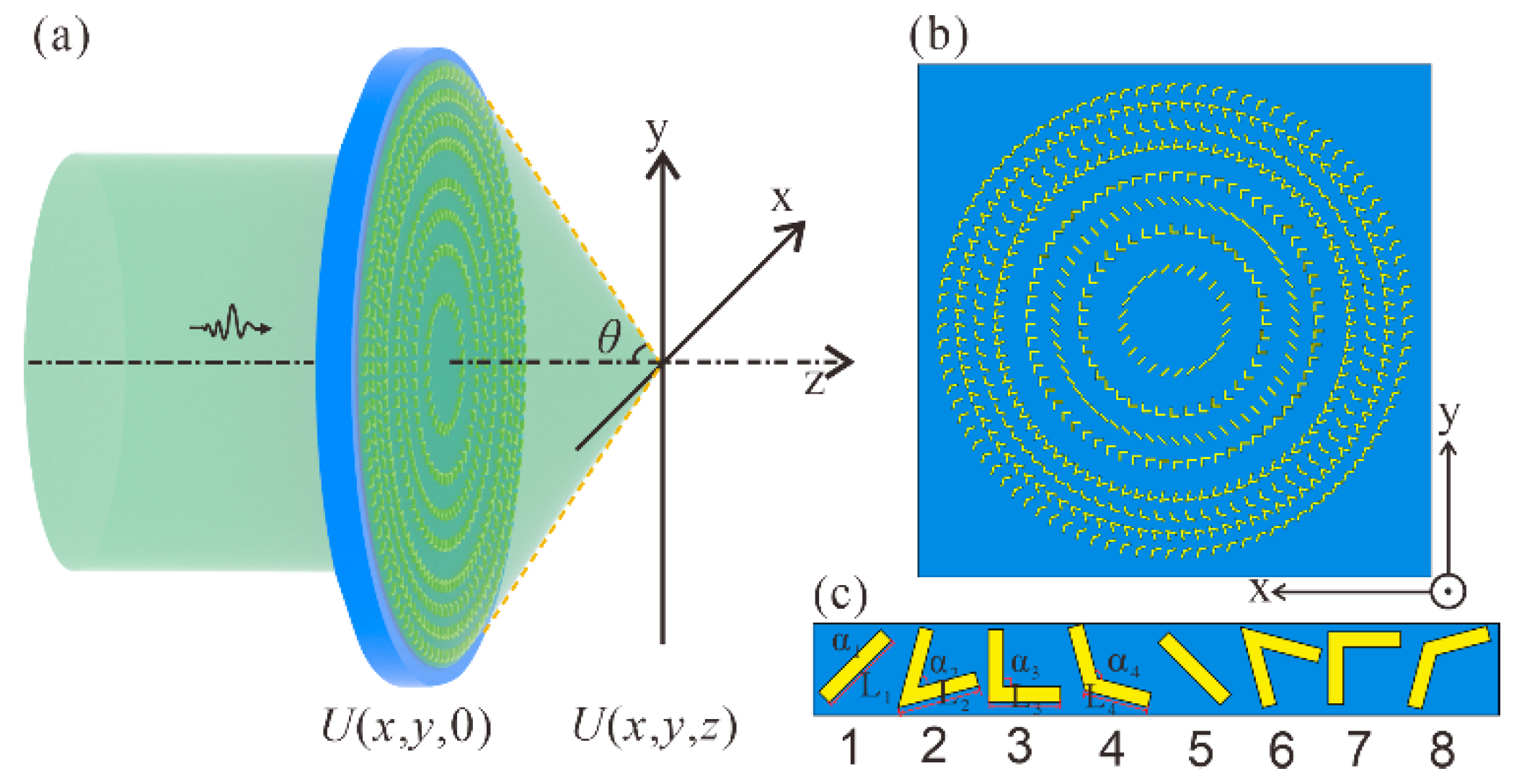
Figure 1a,b presents the schematic of the proposed metalens structure, from the perspective and front views, respectively, which comprises an array of different resonant antenna units distributing on the silicon substrate. The super unit cell contains eight different shapes and sizes of anisotropic antenna resonance units, illustrated in Figure 1c, in the order of 1–3–5–7–2–4–6–8. Based on the super unit cells, concentric rings on the silicon substrate are constructed to form metalens and realize broadband focusing on the x–y plane.
As is well known, the metasurface anisotropic resonant unit in Figure 1b can offer cross-polarized scattering and steer THz wave in directions characterized by the generalized Snell’s theorem. To realize focus, the eight resonant units in super unit cells of concentric rings should be arranged in a special pattern. The required phase shift ψ(r) at a distance of r from the center of the metalens should be as follows:
where f is the focal length of the designed metalens, and λ is the wavelength of the incident THz wave in free space. Practically, the spatial resolution in the metalens system can be analyzed by the angular spectrum model [28]. Since a wave is an incident on a transverse (x,y) plane traveling along the z direction with U(x,y,0) representing the complex field across the z = 0 plane where the lens is located, the angular spectrum A(fX, fY, 0) of U(x,y,0) can be given by
where fX and fY are spatial frequencies. According to angular spectrum model, the angular spectrum A(fX,fY,z) at distance z can be written by A(fX,fY,0) multiplying transfer function H(fX,fY), i.e., . The complex field U(fX,fY,z) at z can be written as an inverse Fourier transform of A(fX,fY,z),
Nonetheless, considering that the lens structure with a finite size limits the extent of the filed distribution, U(x,y,0) should be rewritten as
with
Thus, A(x, y, 0) in Equation (2) will be
Then, the angular spectrum at distance z becomes .
Subsequently, the complex field at z should be given by
It is clear that the circ(x,y) function in Equation (5) has an effect on the angular spectrum , and finally, on the field distribution of in Equation (6). Generally, the smaller the radius of the metalenses at z = 0 is, i.e., the smaller the r of circ function in Equation (4), the broader the FWHM of field distribution .
3. Simulation Results and Discussion
Specifically, the substrate of the metalens in Figure 1 is set as silicon with a dielectric constant of 11.7 and thickness of 200 μm. The material of resonance units is copper with a thickness of 0.2 μm. The linearly polarized THz wave (electric field along the x axis) is a normal incident along the z direction. We first performed numerical simulations through CST Studio Suite to realize metalens focusing by optimizing the geometric parameters of the structure. We took 1.1 THz (corresponding to wavelength 273 μm) as an example, for which the periodicity length is px = py = 58 μm. The parameters characterizing the units from 1 to 4 are L1 = 58 μm, L2 = 57.9 μm, L3 = 47.8 μm, L4 = 42.8 μm and α1 = 0°, α2 = 60°, α3 = 90°, α4 = 120°. Here, Li and αi (I = 1,2,3,4) are the arm lengths and angles of the units shown in Figure 1c, respectively. Units from 5 to 8 were separately obtained by rotating units 1–4 by an angle of 90° clockwise. The width of each unit arm is w = 10 µm. Figure 2a displays simulation results of transmittance and phase values of the eight resonant units in each super unit cell [29,30] at 1.1 THz. We can find that the eight units have similar transmittance (the red line) and geometric phases cover from 0 to 2π (the black line) by π/4 step, ensuring that the transmitted wavefront approximates a plane wave. In Figure 2b, the solid curve demonstrates the relation of required phases and r in Equation (1), and the red points indicate the actual phase that can be provided by distributed resonance units in metalens of Figure 1.
Furthermore, the distribution of electric field intensity for cross-polarized THz wave (electric field is along the y axis) on metalens can be obtained through CST. To analyze the spatial resolution of the metalens conventionally, we first define numerical aperture (NA) as NA = n*sin(θ), in which n is the refractive index of air, and θ is dominated by radius r and focal length f of metalens shown in Figure 1. Practically, for metalenses with certain designed superunit cells, the f will keep unchanged and different r offers different NA. Meanwhile, different r leads to different circ(x,y) functions in Equation (4), and as a result, a different spatial resolution of angular spectrum model. In other words, larger r provides larger NA and smaller FWHM of field distribution, i.e., higher spatial resolution. Specifically, the distribution for metalens with r = 1135 μm is shown in Figure 3a, while the front view is shown in Figure 3e. From Figure 3a, we can infer that the focal length for 1.1 THz is approximately 1000 μm, and NA = 0.79 can be obtained. At the focal plane (z = 1000 μm), the electric field distribution |Ey| along the x axis is illustrated in Figure 3i by a black solid curve, which shows that FWHM = 205 µm. When r = 1877 μm, 2515 μm, and 3131 μm, corresponding to NA = 0.89, 0.93, and 0.95, the electric field distributions with views of x–z and x–y planes are shown in Figure 3b–d,f–h, respectively. In addition, at the focal plane (z = 1000 μm), the electric field distributions along the x axis are severally illustrated in Figure 3i by solid, dotted, triangle, and square curves with NA = 0.95, 0.93, 0.89, and 0.79, respectively. Correspondingly, the FWHMs depending on r are shown in Figure 3j. It is shown that larger r leads to smaller FWHM in Figure 3j and higher spatial resolution in Figure 3a–d, that is, in practical application, the performance of metalenses for THz imaging, communication, photonic integrated circuits is affected by the set of r. Additionally, the focusing efficiency can be defined as energy ratio of center focusing spot to the incidence, which is 5.1%, 5.2%, 3.73%, 2.7% for NA = 0.78, 0.85, 0.92, and 0.95, respectively [31].
4. Experimental Results
The V-shaped units of metalenses were fabricated on the silicon substrate by UV lithography. First, a layer of 10 nm thick chromium was deposited on the silicon substrate with an electron beam evaporator, followed by the depositing of 200 nm thick copper on it. Then, positive photoresist SUN-115P was coated onto the silicon substrate by a spin coater at a spin speed of 2000 rpm for 30 s, followed by hot plate baking at 100 °C for 1 min. Next, the V-shaped antennas were defined on photoresist surface by UV lithography, followed by hot plate baking at 100 °C for 90 s. After photoresist development in SUN-238D for 8 s, copper was etched excess from the sample by reactive ion etching. The last step to pattern the designed structure was a liftoff process in the acetone to remove photoresist from the surface of the structure. Figure 4a shows the microscopic image of the fabricated sample. We performed the measurement by THz near-field imaging system (TeraCube Scientific M2), as illustrated in Figure 4b. The fs-laser source we used is 780 nm with 100 fs pulse width and 80 MHz repetition rate. The THz signal scans the sample surface using a microprobe and is recorded at each pixel to obtain a THz image. The measured electric field distributions for metalenses with r = 1135 μm, 1877 μm, 2515 μm, and 3131 μm, corresponding to NA = 0.79, 0.89, 0.93, and 0.95, are shown in Figure 4c–f, respectively. During the measurement process, the microprobe of the system kept a 1000 μm distance from metalens samples. Through Figure 4c–f, the electric field distributions along the x axis are severally obtained and illustrated in Figure 4g. Correspondingly, the relations between FWHMs and r are demonstrated in Figure 4h, which shows that FWHM decreases from 343 μm to 206 μm as NA increases from 0.79 to 0.95. Clearly, the experimental results in Figure 4c–h agree well with the simulation results in Figure 3e–j and the analysis of the angular spectral model, demonstrating that larger r, i.e., larger NA, leads to smaller FWHM and higher spatial resolution. Here, we note that in Figure 4c–f, the background signals are mainly affected by the copolarized transmission. Additionally, the focusing efficiency of 3.7%, 4.19%, 3.17%, and 2.4% for NA = 0.78, 0.85, 0.92, and 0.95 are achieved, respectively. Compared to the 3% focusing efficiency in [32], similar efforts are obtained in our structure. Nonetheless, metasurfaces consists of Si Mie resonators can provide almost lossless transmission [33], implying the possibility of our next investigation.
5. Conclusions
In conclusion, metalenses comprising arrays of different V-shaped antenna units distributing on a silicon substrate are proposed theoretically and fabricated experimentally. We first performed numerical simulations, and the results show that a larger numerical aperture of metalenses can provide a smaller FWHM of field distribution, leading to higher spatial resolution. Then, we experimentally fabricated the metalenses samples by UV lithography and measured their field distributions by THz near-field imaging system. The experimental results agree very well with numerical prediction. Our proposed design can facilitate the practical application of metalenses in THz imaging, communication, photonic integrated circuits, etc.
Author Contributions
Conceptualization, X.Y. and Y.S.; methodology, X.Y.; software, X.Y. and T.Z.; validation, G.D., Y.S. and L.Z.; formal analysis, Y.S.; investigation, X.Y.; resources, Y.S.; data curation, X.Y.; writing—original draft preparation, X.Y.; writing—review and editing, Y.S.; funding acquisition, Y.S. and X.D. All authors have read and agreed to the published version of the manuscript.
Funding
This work was supported by the National Natural Science Foundation of China (Grant numbers 61865009, 61927813).
Institutional Review Board Statement
Not applicable.
Informed Consent Statement
Not applicable.
Data Availability Statement
Data are available from the authors on request.
Conflicts of Interest
The authors declare no conflict of interest.
References
- Chen, S.; Li, Z.; Zhang, Y.; Cheng, H.; Tian, J. Phase Manipulation of Electromagnetic Waves with Metasurfaces and Its Applications in Nanophotonics. Adv. Opt. Mater. 2018, 6, 1800104. [Google Scholar] [CrossRef]
- Grady, N.K.; Heyes, J.E.; Chowdhury, D.R.; Zeng, Y.; Reiten, M.T.; Azad, A.K.; Taylor, A.J.; Dalvit, D.A.; Chen, H.T. Terahertz metamaterials for linear polarization conversion and anomalous refraction. Science 2013, 340, 1304–1307. [Google Scholar] [CrossRef] [PubMed] [Green Version]
- Chen, X.; Huang, L.; Mühlenbernd, H.; Li, G.; Bai, B.; Tan, Q.; Jin, G.; Qiu, C.W.; Zhang, S.; Zentgraf, T. Dual-polarity plasmonicmetalens for visible light. Nat. Commun. 2012, 3, 1–6. [Google Scholar] [CrossRef]
- Ma, C.; Liu, Z. A super resolution metalens with phase compensation mechanism. Appl. Phys. Lett. 2010, 96, 183103. [Google Scholar] [CrossRef] [Green Version]
- Williams, C.; Montelongo, Y.; Wilkinson, T.D. PlasmonicMetalens for Narrowband Dual-Focus Imaging. Adv. Opt. Mater. 2017, 5, 1700811. [Google Scholar] [CrossRef]
- Ni, X.; Ishii, S.; Kildishev, A.V.; Shalaev, V.M. Ultra-thin, planar, Babinet-inverted plasmonicmetalenses. Light Sci. Appl. 2013, 2, e72. [Google Scholar] [CrossRef]
- Hu, D.; Wang, X.; Feng, S.; Ye, J.; Sun, W.; Kan, Q.; Klar, P.J.; Zhang, Y. Ultrathin Terahertz Planar Elements. Adv. Opt. Mater. 2013, 1, 186–191. [Google Scholar] [CrossRef] [Green Version]
- Liu, Z.; Lee, H.; Xiong, Y.; Sun, C.; Zhang, X. Far-field optical hyperlens magnifying sub-diffraction-limited objects. Science 2007, 315, 1686. [Google Scholar] [CrossRef] [Green Version]
- Fang, N.; Lee, H.; Sun, C.; Zhang, X. Sub-Diffraction-Limited Optical Imaging with a Silver Superlens. Science 2005, 5721, 534–537. [Google Scholar] [CrossRef] [PubMed] [Green Version]
- Berweger, S.; Atkin, J.M.; Olmon, R.L.; Raschke, M.B. Adiabatic Tip-Plasmon Focusing for Nano-Raman Spectroscopy. J. Phys. Chem. Lett. 2010, 1, 3427–3432. [Google Scholar] [CrossRef]
- Manikandan, E.; Sreeja, B.S.; Radha, S.; Bathe, R.N. Direct laser fabrication of five-band symmetric terahertz metamaterial with Fano resonance. Mater. Lett. 2018, 229, 320–323. [Google Scholar] [CrossRef]
- Yang, C.; Shen, Y.; Xie, Y.; Zhou, Q.; Deng, X.; Cao, J. Terahertz planar lenses based on plasmonicmetasurfaces. Phys. Lett. A 2019, 383, 789–792. [Google Scholar] [CrossRef]
- Zhang, F.; Yu, H.; Fang, J.; Zhang, M.; Chen, S.; Wang, J.; He, A.; Chen, J. Efficient generation and tight focusing of radially polarized beam from linearly polarized beam with all-dielectric metasurface. Opt. Express 2016, 24, 6656. [Google Scholar] [CrossRef] [PubMed] [Green Version]
- Fattal, D.; Li, J.; Peng, Z.; Fiorentino, M.; Beausoleil, R.G. Flat dielectric grating reflectors with focusing abilities. Nat. Photonics 2010, 4, 466–470. [Google Scholar] [CrossRef] [Green Version]
- Yu, N.; Genevet, P.; Kats, M.A.; Aieta, F.; Tetienne, J.P.; Capasso, F.; Gaburro, Z. Light Propagation with Phase Discontinuities: Generalized Laws of Reflection and Refraction. Science 2011, 334, 333–337. [Google Scholar] [CrossRef] [PubMed] [Green Version]
- Gao, H.; Pu, M.; Li, X.; Ma, X.; Zhao, Z.; Guo, Y.; Luo, X. Super-resolution imaging with a Bessel lens realized by a geometric metasurface. Opt. Express 2017, 25, 13933–13943. [Google Scholar] [CrossRef] [PubMed]
- Jiang, R.H.; Chen, C.; Lin, D.Z.; Chou, H.C.; Chu, J.Y.; Yen, T.J. Near-Field Plasmonic Probe with Super Resolution and High Throughput and Signal-to-Noise Ratio. Nano Lett. 2018, 18, 881–885. [Google Scholar] [CrossRef]
- Khorasaninejad, M.; Chen, W.T.; Oh, J.; Capasso, F. Super-Dispersive Off-Axis Meta-Lenses for Compact High Resolution Spectroscopy. Nano Lett. 2016, 16, 3732–3737. [Google Scholar] [CrossRef]
- Khorasaninejad, M.; Chen, W.T.; Devlin, R.C.; Oh, J.; Zhu, A.Y.; Capasso, F. Metalenses at visible wavelengths: Diffraction-limited focusing and subwavelength resolution imaging. Science 2016, 4, 352–1190. [Google Scholar] [CrossRef] [Green Version]
- Xie, Y.; Yang, C.; Wang, Y.; Shen, Y.; Deng, X.; Zhou, B.; Cao, J. Anomalous refraction and reflection characteristics of bend V-shaped antenna metasur faces. Sci. Rep. 2019, 9, 1–8. [Google Scholar] [CrossRef] [Green Version]
- Blanchard, R.; Aoust, G.; Genevet, P.; Yu, N.; Kats, M.A.; Gaburro, Z.; Capasso, F. Modeling nanoscale V-shaped antennas for the design of optical phased arrays. Phys. Rev. B 2012, 85, 155457. [Google Scholar] [CrossRef] [Green Version]
- Aieta, F.; Genevet, P.; Yu, N.; Kats, M.A.; Gaburro, Z.; Capasso, F. Out-of-Plane Reflection and Refraction of Light by Anisotropic Optical Antenna Metasurfaces with Phase Discontinuities. Nano Lett. 2012, 12, 1702–1706. [Google Scholar] [CrossRef]
- Wen, D.; Yue, F.; Kumar, S.; Ma, Y.; Chen, M.; Ren, X.; Kremer, P.E.; Gerardot, B.D.; Taghizadeh, M.R.; Buller, G.S.; et al. Metasurface for characterization of the polarization state of light. Opt. Express 2015, 23, 10272. [Google Scholar] [CrossRef] [PubMed]
- Fan, Q.; Huo, P.; Wang, D.; Liang, Y.; Yan, F.; Xu, T. Visible light focusing flat lenses based on hybrid dielectric-metal metasurface reflector-arrays. Sci. Rep. 2017, 7, 1–9. [Google Scholar] [CrossRef] [PubMed]
- Ding, P.; Li, Y.; Shao, L.; Tian, X.; Wang, J.; Fan, C. Graphene aperture-based metalens for dynamic focusing of terahertz waves. Opt. Express 2018, 26, 28038–28050. [Google Scholar] [CrossRef]
- Ramm, A.G. Does negative refraction make a perfect lens. Phys. Rev. Lett. 2008, 372, 6518–6520. [Google Scholar] [CrossRef] [Green Version]
- Tan, Q.; Xu, Z.; Zhang, D.H.; Yu, T.; Zhang, S.; Luo, Y. Polarization-Controlled Plasmonic Structured Illumination. Nano Lett. 2020, 20, 2602–2608. [Google Scholar] [CrossRef] [PubMed]
- Richards, B.; Wolf, E. Electromagnetic Diffraction in Optical Systems. II. Structure of the Image Field in an Aplanatic System. Proc. R. Soc. Lond. Ser. A Math. Phys. Sci. 1959, 253, 358–379. [Google Scholar] [CrossRef]
- Huang, F.M.; Kao, T.S.; Fedotov, V.A.; Chen, Y.; Zheludev, N.I. Nanohole Array as a Lens. Nano Lett. 2008, 8, 2469–2472. [Google Scholar] [CrossRef] [PubMed] [Green Version]
- Ullah, N.; Liu, W.; Wang, G.; Wang, Z.; Khalid, A.U.R.; Hu, B.; Liu, J.; Zhang, Y. Gate-controlled terahertz focusing based on graphene-loaded metasurface. Opt. Express 2020, 28, 2789. [Google Scholar] [CrossRef] [PubMed]
- Cheng, Q.; Ma, M.; Yu, D.; Shen, Z.; Xie, J.; Wang, J.; Xu, N.; Guo, H.; Hu, W.; Wang, S.; et al. Broadband achromatic metalens in terahertz regime. Sci. Bull. 2019, 64, 1525–1531. [Google Scholar] [CrossRef] [Green Version]
- Cai, H.; Czaplewski, D.; Ogando, K.; Martinson, A.; Gosztola, D.; Stan, L.; López, D. Ultrathin transmissive metasurfaces for multi-wavelength optics in the visible. Appl. Phys. Lett. 2019, 114, 71106. [Google Scholar] [CrossRef]
- Dharmavarapu, R.; Izumi, K.I.; Katayama, I.; Ng, S.H.; Vongsvivut, J.; Tobin, M.J.; Kuchmizhak, A.; Nishijima, Y.; Bhattacharya, S.; Juodkazis, S. Dielectric cross-shaped-resonator-based metasurface for vortex beam generation at mid-IR and THz wavelengths. Nanophotonics 2019, 8, 1263–1270. [Google Scholar] [CrossRef] [Green Version]
Figure 1.
Schematic of the metalens sample with (a) perspective and (b) front views. The super unit cell of the metalens consists of eight antenna units (c) in the order of 1–3–5–7–2–4–6–8. Parameters of units 1–4 are L1 = 58 μm, L2 = 57.9 μm, L3 = 47.8 μm, L4 = 42.8 μm and α1 = 0°, α2 = 60°, α3 = 90°, α4 = 120°, respectively. Units 5–8 were separately obtained by rotating units 1–4 by an angle of 90° clockwise.

Figure 2.
(a) Numerical results of transmittance and phase values of the eight resonant units in each super unit cell at 1.1 THz. The black curve shows the phase of cross-polarized scatter, and the red curve shows transmittance. (b) The solid curve shows the required phase, which is calculated from Equation (1) at 1.1 THz, and the red dot shows the phase that can be actually provided by resonance units.

Figure 3.
(a–h) Numerical results of the metalens with NA = 0.79, 0.89, 0.93 and 0.95, corresponding to r = 1135 μm, 1877 μm, 2515 μm, and 3131 μm, respectively. Electric field distributions with views on x–z and x–y planes are severally shown in (a–d) and (e–h). (i) The electric field distributions along the x axis at the focal plane. (j) The relationship between FWHMs and r.

Figure 4.
(a) Microscope image of fabricated metalens sample. (b) Schematic of the THz near-field imaging system. (c–f) Experimentally obtained electric field distributions of metalens with NA = 0.79, 0.89, 0.93, and 0.95, corresponding to r = 1135 μm, 1877 μm, 2515 μm, and 3131 μm, respectively. (g) The electric field distributions along the x axis at the focal plane. (h) The relationship between FWHMs and r.

Publisher’s Note: MDPI stays neutral with regard to jurisdictional claims in published maps and institutional affiliations. |
© 2021 by the authors. Licensee MDPI, Basel, Switzerland. This article is an open access article distributed under the terms and conditions of the Creative Commons Attribution (CC BY) license (https://creativecommons.org/licenses/by/4.0/).
Share and Cite
MDPI and ACS Style
Yu, X.; Shen, Y.; Dai, G.; Zou, L.; Zhang, T.; Deng, X. Phase-Controlled Planar Metalenses for High-Resolution Terahertz Focusing. Photonics 2021, 8, 143. https://0-doi-org.brum.beds.ac.uk/10.3390/photonics8050143
AMA Style
Yu X, Shen Y, Dai G, Zou L, Zhang T, Deng X. Phase-Controlled Planar Metalenses for High-Resolution Terahertz Focusing. Photonics. 2021; 8(5):143. https://0-doi-org.brum.beds.ac.uk/10.3390/photonics8050143
Chicago/Turabian StyleYu, Xin, Yun Shen, Guohong Dai, Liner Zou, Tailin Zhang, and Xiaohua Deng. 2021. "Phase-Controlled Planar Metalenses for High-Resolution Terahertz Focusing" Photonics 8, no. 5: 143. https://0-doi-org.brum.beds.ac.uk/10.3390/photonics8050143
Note that from the first issue of 2016, this journal uses article numbers instead of page numbers. See further details here.