Efficient Carrier Recombination in InGaN Pyramidal µ-LEDs Obtained through Selective Area Growth

 and
and 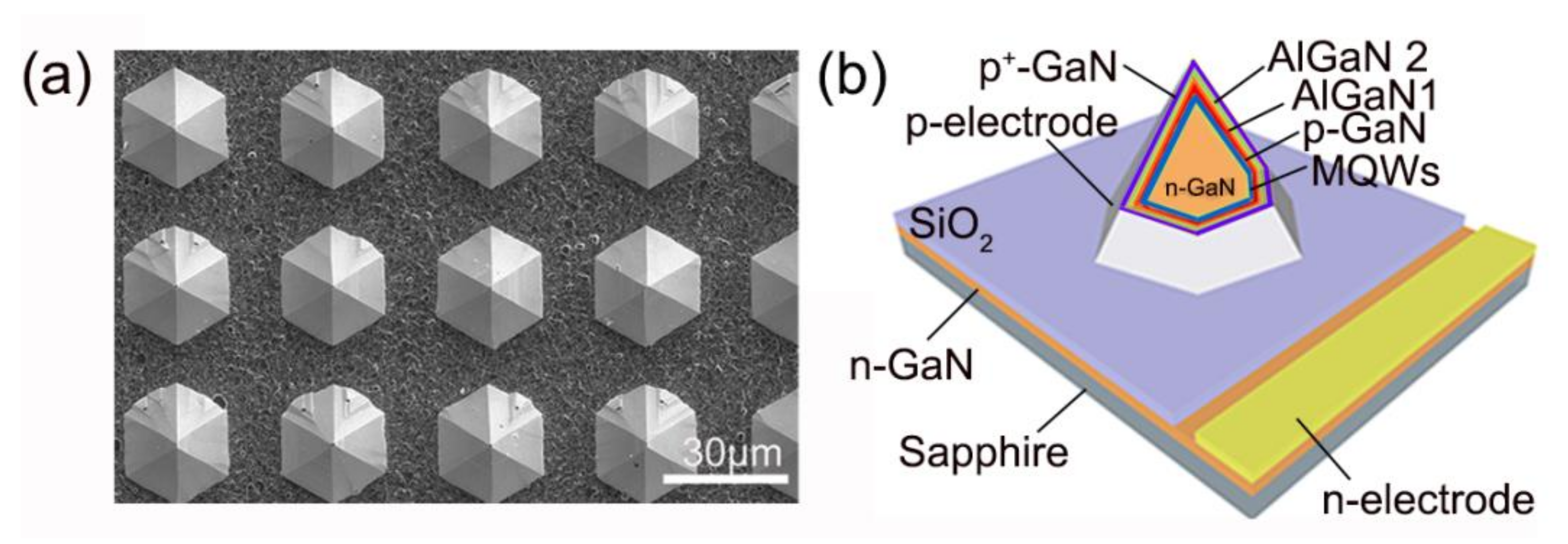
Abstract
:1. Introduction
2. Materials and Methods
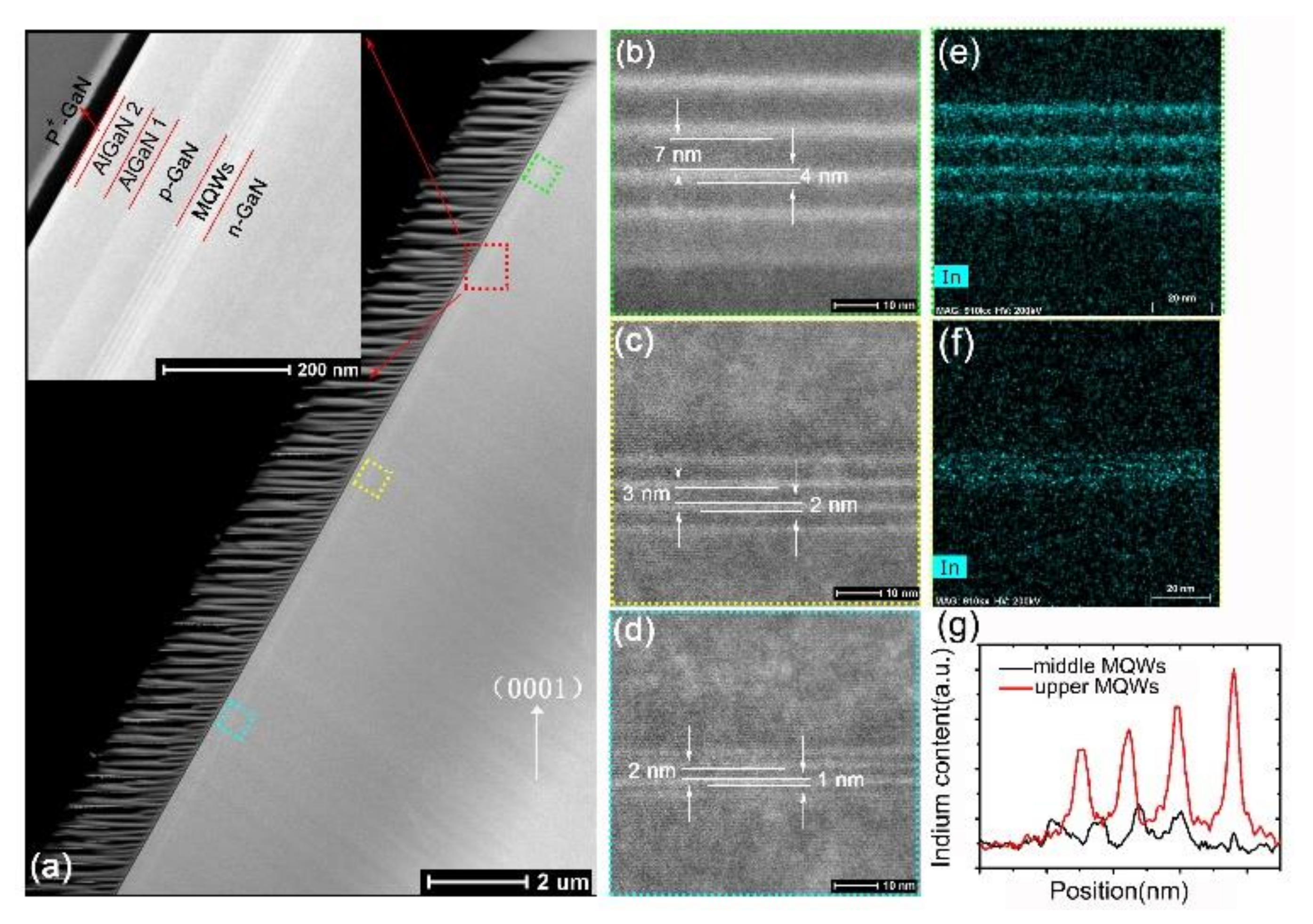
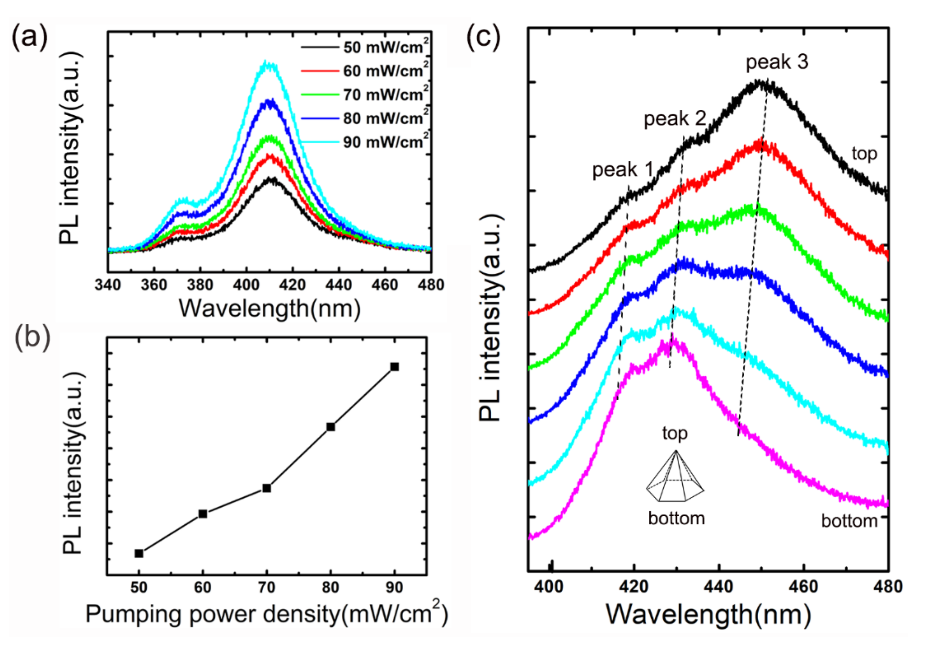
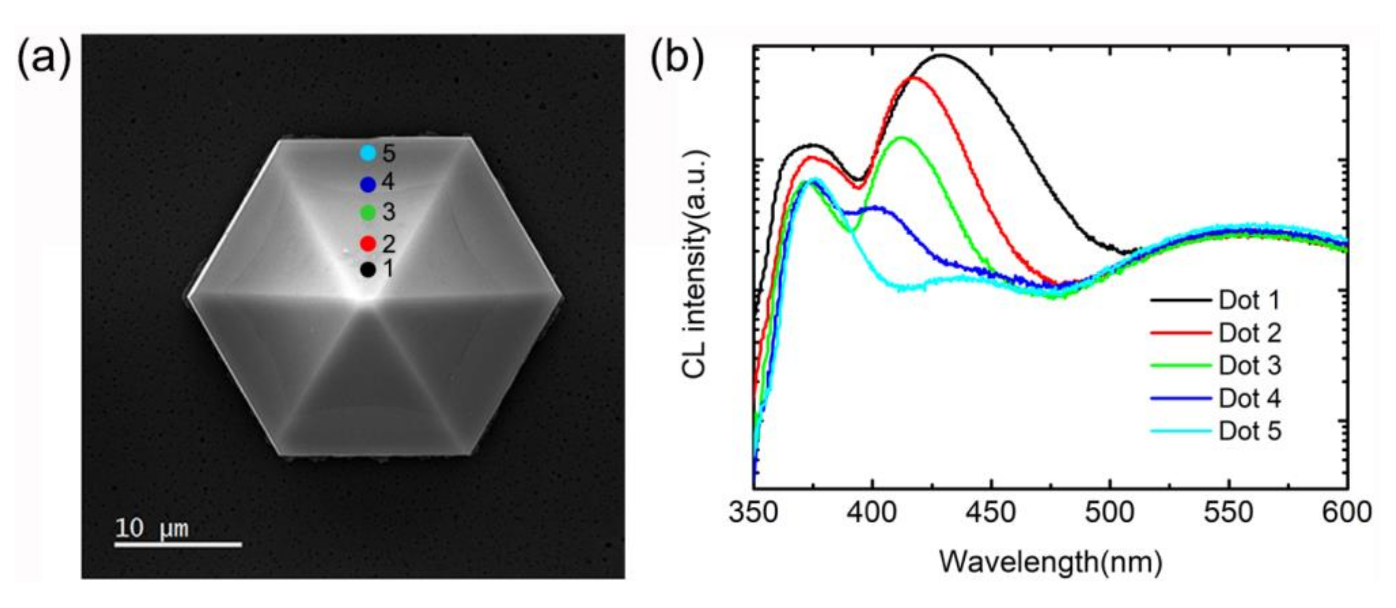
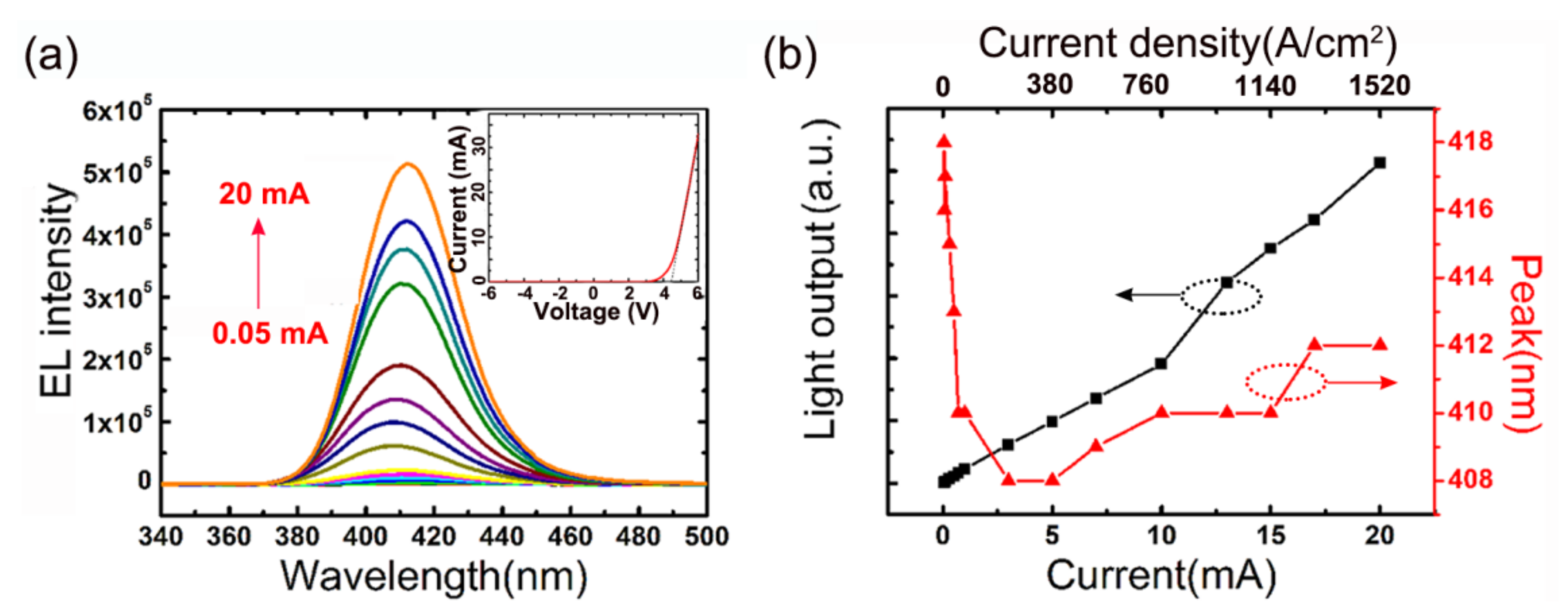
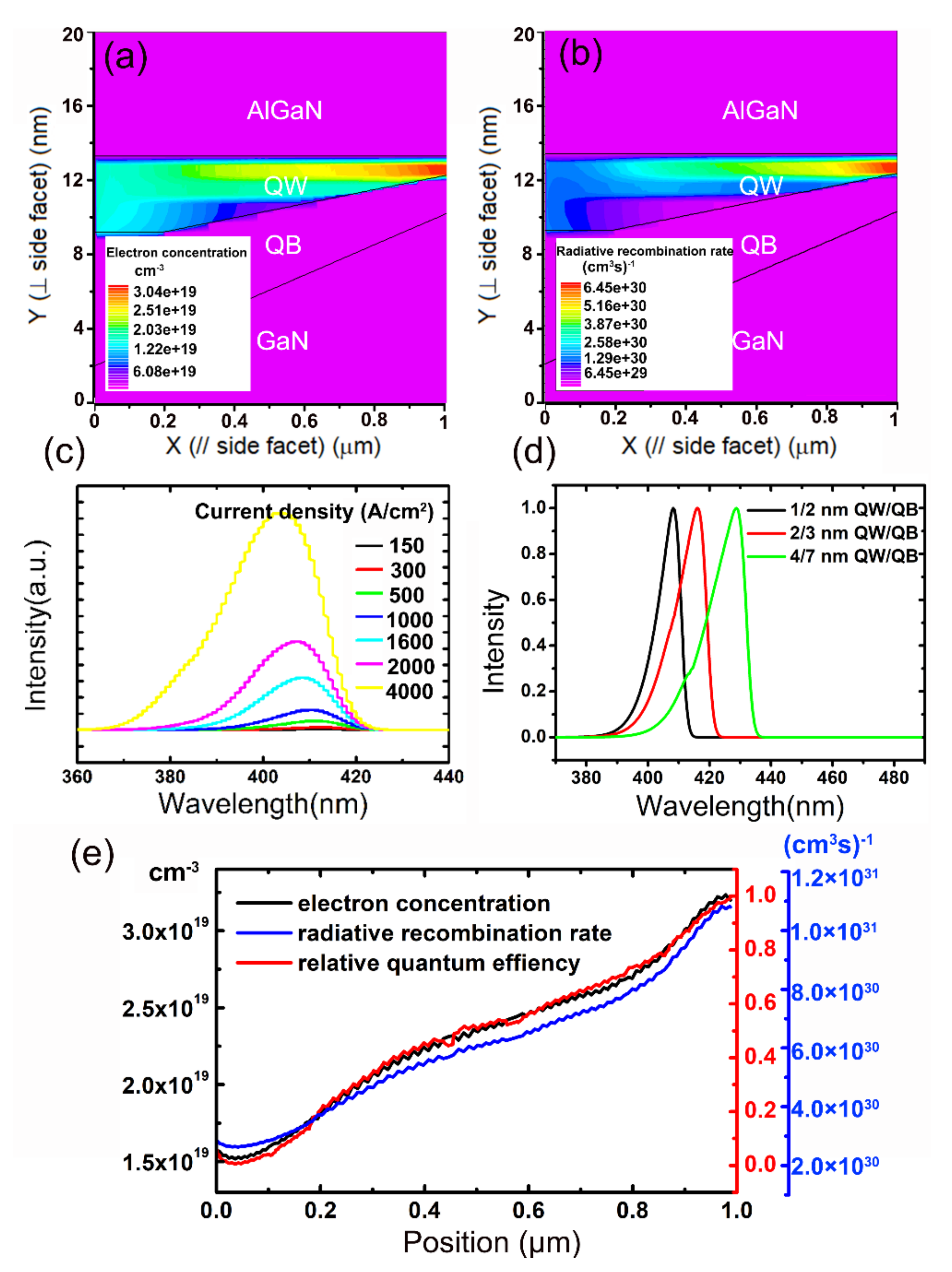
3. Results
4. Conclusions
Supplementary Materials
Author Contributions
Funding
Data Availability Statement
Conflicts of Interest
References
- Li, K.H.; Liu, X.; Wang, Q.; Zhao, S.; Mi, Z. Ultralow-threshold electrically injected AlGaN nanowire ultraviolet lasers on Si operating at low temperature. Nat. Nanotechnol. 2015, 10, 140–144. [Google Scholar] [CrossRef] [PubMed]
- Hou, Y.; Renwick, P.; Liu, B.; Bai, J. Room temperature plasmonic lasing in a continuous wave operation mode from an InGaN/GaN single nanorod with a low threshold. Sci. Rep. 2014, 4, 5014. [Google Scholar] [CrossRef] [PubMed] [Green Version]
- Koester, R.; Hwang, J.S.; Salomon, D.; Chen, X.; Bougerol, C.; Barnes, J.P.; Dang, D.; Rigutti, L.; Bugallo, A.d.; Jacopin, G.; et al. M-plane core-shell InGaN/GaN multiple-quantum-wells on gan wires for electroluminescent devices. Nano Lett. 2011, 11, 4839–4845. [Google Scholar] [CrossRef]
- Tian, P.; McKendry, J.J.D.; Gong, Z.; Zhang, S.; Watson, S.; Zhu, D.; Watson, I.M.; Gu, E.; Kelly, A.E.; Humphreys, C.J.; et al. Characteristics and applications of micro-pixelated GaN-based light emitting diodes on Si substrates. J. Appl. Phys. 2014, 115, 013103. [Google Scholar] [CrossRef]
- Ley, R.T.; Smith, J.M.; Wong, M.S.; Margalith, T.; Gordon, M.J. Revealing the importance of light extraction efficiency in InGaN/GaN microleds via chemical treatment and dielectric passivation. Appl. Phys. Lett. 2020, 116, 251104. [Google Scholar] [CrossRef]
- Krylyuk, S.; Paramanik, D.; King, M.; Motayed, A.; Ha, J.Y.; Bonevich, J.E.; Talin, A.; Davydov, A.V. Large-area GaN n-core/p-shell arrays fabricated using top-down etching and selective epitaxial overgrowth. Appl. Phys. Lett. 2012, 101, 071101. [Google Scholar] [CrossRef] [Green Version]
- Krylyuk, S.; Debnath, R.; Yoon, H.P.; King, M.R.; Ha, J.Y.; Wen, B.; Motayed, A.; Davydov, A.V. Faceting control in core-shell GaN micropillars using selective epitaxy. Appl. Mater. 2014, 2, 071101. [Google Scholar] [CrossRef] [Green Version]
- Wong, M.S.; Hwang, D.; Alhassan, A.I.; Lee, C.; Ley, R.; Nakamura, S.; DenBaars, S.P. High efficiency of III-nitride micro-light-emitting diodes by sidewall passivation using atomic layer deposition. Opt. Express 2018, 26, 21324–21331. [Google Scholar] [CrossRef] [PubMed]
- Waag, A.; Wang, X.; Fündling, S.; Ledig, J.; Erenburg, M.; Neumann, R.; Suleiman, M.A.; Merzsch, S.; Wei, J.; Li, S.; et al. The nanorod approach: GaN Nano-LEDs for solid state lighting. Phys. Status Solidi C 2011, 8, 2296–2301. [Google Scholar] [CrossRef]
- Jung, B.O.; Bae, S.Y.; Kato, Y.; Imura, M.; Amano, H. Morphology development of GaN nanowires using a pulsed-mode MOCVD growth technique. CrystEngComm 2014, 16, 2273–2282. [Google Scholar] [CrossRef]
- Lin, Y.T.; Yeh, T.W.; Daniel, D.P. Mechanism of selective area growth of GaN nanorods by pulsed mode metalorganic chemical vapor deposition. Nanotechnology 2012, 23, 465601. [Google Scholar] [CrossRef]
- Bergbauer, W.; Strassburg, M.; Kölper, C.; Linder, N.; Roder, C.; Lähnemann, J.; Trampert, A.; Fündling, S.; Li, S.F.; Wehmann, H.H.; et al. Continuous-flux MOVPE growth of position-controlled n-face GaN nanorods and embedded InGaN quantum wells. Nanotechnology 2010, 21, 305201. [Google Scholar] [CrossRef]
- Bae, S.Y.; Lekhal, K.; Lee, H.J.; Min, J.W.; Lee, D.S.; Honda, Y.; Amano, H. Selective-area growth of doped GaN nanorods by pulsed-mode MOCVD: Effect of Si and Mg dopants. Phys. Status Solidi B 2017, 254, 1600722. [Google Scholar] [CrossRef]
- Jiang, J.; Xu, H.; Sheikhi, M.; Li, L.; Yang, Z.; Hoo, J.; Guo, S.; Zeng, Y.; Guo, W.; Ye, J. Omnidirectional whispering-gallery-mode lasing in GaN microdisk obtained by selective area growth on sapphire substrate. Opt. Express 2019, 27, 16195–16205. [Google Scholar] [CrossRef] [Green Version]
- Bae, S.Y.; Jung, B.O.; Lekhal, K.; Kim, S.Y.; Lee, J.Y.; Lee, D.S.; Deki, M.; Honda, Y.; Amano, H. Highly elongated vertical GaN nanorod arrays on Si substrates with an AlN seed layer by pulsed-mode metal-organic vapor deposition. CrystEngComm 2016, 18, 1505–1514. [Google Scholar] [CrossRef]
- Choi, K.; Arita, M.; Arakawa, Y. Selective-area growth of thin GaN nanowires by MOCVD. J. Cryst. Growth 2012, 357, 58–61. [Google Scholar] [CrossRef]
- Hiramatsu, K.; Nishiyama, K.; Motogaito, A. Recent Progress in Selective Area Growth and Epitaxial Lateral Overgrowth of III-Nitrides: Effects of Reactor Pressure in MOVPE Growth. Phys. Status Solidi A 1999, 176, 535–543. [Google Scholar] [CrossRef]
- Li, C.; Wright, J.B.; Liu, S.; Lu, P.; Figiel, J.J.; Leung, B.; Chow, W.W.; Brener, I.; Koleske, D.D.; Luk, T.; et al. Nonpolar InGaN/GaN core–shell single nanowire lasers. Nano Lett. 2017, 17, 1049–1055. [Google Scholar] [CrossRef] [PubMed]
- Nami, M.; Stricklin, I.E.; DaVico, K.M.; Masabih, S.M.; Rishinaramangalam, A.K.; Brueck, S.R.J.; Brener, I.; Feezell, D.F. Carrier Dynamics and Electro-Optical Characterization of High-Performance GaN/InGaN Core-Shell Nanowire Light-Emitting Diodes. Sci. Rep. 2018, 8, 1–11. [Google Scholar] [CrossRef] [PubMed] [Green Version]
- Li, S.F.; Fuendling, S.; Wang, X.; Merzsch, S.; Al-Suleiman, M.A.M.; Wei, J.D.; Wehmann, H.H.; Waag, A.; Bergbauer, W.; Strassburg, M. Polarity and its influence on growth mechanism during MOVPE growth of GaN sub-micrometer rods. Cryst. Growth Des. 2011, 11, 1573–1577. [Google Scholar] [CrossRef]
- Yamano, K.; Kishino, K.; Sekiguchi, H.; Oto, T.; Wakahara, A.; Kawakami, Y. Novel selective area growth (SAG) method for regularly arranged AlGaN nanocolumns using nanotemplates. J. Cryst. Growth 2015, 425, 316–321. [Google Scholar] [CrossRef]
- Robin, Y.; Liao, Y.; Pristovsek, M.; Amano, H. Simultaneous growth of various InGaN/GaN core-shell microstructures for color tunable device applications. Phys. Status Solidi A 2018, 215, 1800361. [Google Scholar] [CrossRef]
- Bryan, I.; Bryan, Z.; Mita, S.; Rice, A.; Tweedie, J.; Collazo, R.; Sitar, Z. Surface kinetics in AlN growth: A universal model for the control of surface morphology in III-nitrides. J. Cryst. Growth 2016, 438, 81–89. [Google Scholar] [CrossRef] [Green Version]
- Wunderer, T.; Feneberg, M.; Lipski, F.; Wang, J.; Leute, R.A.R.; Schwaiger, S.; Thonke, K.; Chuvilin, A.; Kaiser, U.; Metzner, S.; et al. Three-dimensional GaN for semipolar light emitters. Phys. Status Solidi B 2010, 248, 549–560. [Google Scholar] [CrossRef]
- Edwards, P.R.; Martin, R.W.; Watson, I.M.; Liu, C.; Taylor, R.A.; Rice, J.H.; Na, J.H.; Robinson, J.W.; Smith, J.D. Quantum dot emission from site-controlled InGaN/GaN micropyramid arrays. Appl. Phys. Lett. 2014, 85, 4281–4283. [Google Scholar] [CrossRef] [Green Version]
- Liu, W.; Mounir, C.; Rossbach, G.; Schimpke, T.; Avramescu, A.; Lugauer, H.-J.; Strassburg, M.; Schwarz, U.; Deveaud, B.; Jacopin, G. Spatially dependent carrier dynamics in single InGaN/GaN core-shell microrod by time-resolved cathodoluminescence. Appl. Phys. Lett. 2018, 112, 052106. [Google Scholar] [CrossRef]
- Hoffmann, A.; Siegle, H.; Kaschner, A.; Eckey, L.; Sawaki, N. Local strain distribution of hexagonal GaN pyramids. J. Cryst. Growth 1998, 189, 630–633. [Google Scholar] [CrossRef]
- Tian, P.; Edwards, P.R.; Wallace, M.J.; Martin, R.W.; Mckendry, J.; Gu, E. Characteristics of GaN-based light emitting diodes with different thicknesses of buffer layer grown by HVPE and MOCVD. J. Phys. D Appl. Phys. 2017, 50, 075101. [Google Scholar] [CrossRef] [Green Version]
- Reddy, P.; Hoffmann, M.P.; Kaess, F.; Bryan, Z.; Bryan, I.; Bobea, M.; Klump, A.; Tweedie, J.; Kirste, R.; Mita, S.; et al. Point defect reduction in wide bandgap semiconductors by defect quasi Fermi level control. J. Appl. Phys. 2016, 120, 185704. [Google Scholar] [CrossRef] [Green Version]
- Li, Q.; Wang, G.T. Spatial distribution of defect luminescence in GaN nanowires. Nano Lett. 2010, 10, 1554–1558. [Google Scholar] [CrossRef] [PubMed]
- Zhu, S.; Lin, S.; Li, J.; Yu, Z.; Cao, H.; Yang, C.; Li, J.; Zhao, L. Influence of quantum confined Stark effect and carrier localization effect on modulation bandwidth for GaN-based LEDs. Appl. Phys. Lett. 2017, 111, 171105. [Google Scholar] [CrossRef]
- Tangi, M.; Mishra, P.; Janjua, B.; Prabaswara, A.; Zhao, C.; Priante, D.; Min, J.; Ng, T.K.; Ooi, B.S. Role of quantum-confined stark effect on bias dependent photoluminescence of N-polar GaN/InGaN multi-quantum disk amber light emitting diodes. J. Appl. Phys. 2018, 123, 105702. [Google Scholar] [CrossRef]
- Baek, H.; Lee, C.-H.; Chung, K.; Yi, G.-C. Epitaxial GaN Microdisk Lasers Grown on Graphene Microdots. Nano Lett. 2013, 13, 2782–2785. [Google Scholar] [CrossRef] [PubMed]
- Reshchikov, M.A.; Morkoc, H. Luminescence properties of defects in GaN. J. Appl. Phys. 2005, 97, 061301. [Google Scholar] [CrossRef]
- Debusmann, R.; Brauch, U.; Hoffmann, V.; Weyers, M.; Kneissl, M. Spacer and well pumping of InGaN vertical cavity semiconductor lasers with varying number of quantum wells. J. Appl. Phys. 2012, 112, 033110. [Google Scholar] [CrossRef]
- Chen, W.; Hu, G.; Jiang, J.; Liu, M.; Yang, Y. Electrically Driven Single Pyramid InGaN/GaN Micro Light-Emitting Diode Grown on Silicon Substrate. J. Disp. Technol. 2015, 11, 285–291. [Google Scholar] [CrossRef]
- Chen, W.; Lin, J.; Chen, Y.; Han, X.; Zhang, B. Dual-color ingan/gan pyramidal micro light-emitting diode selectively grown on SiO2 masked Si substrate. J. Disp. Technol. 2015, 12, 1. [Google Scholar] [CrossRef]
- Chung, K.; Yoo, H.; Hyun, J.K.; Oh, H.; Tchoe, Y.; Lee, K.; Baek, H.; Kim, M.; Yi, G.-C. Flexible GaN Light-Emitting Diodes Using GaN Microdisks Epitaxial Laterally Overgrown on Graphene Dots. Adv. Mater. 2016, 28, 7688–7694. [Google Scholar] [CrossRef]
- Bae, S.; Kim, D.; Lee, D.; Lee, S.; Baek, J.H. Highly Integrated InGaN/GaN Semipolar Micro-Pyramid Light-Emitting Diode Arrays by Confined Selective Area Growth. Electrochem. Solid-State Lett. 2012, 15, H47–H50. [Google Scholar] [CrossRef]
- Waltereit, P.; Brandt, O.; Trampert, A.; Grahn, H.T.; Ploog, K.H. Nitride semiconductors free of electrostatic fields for efficient white light-emitting diodes. Nature 2000, 406, 865–868. [Google Scholar] [CrossRef] [PubMed]
- Speck, J.S.; Chichibu, S.F. Nonpolar and Semipolar Group III Nitride-Based Materials. MRS Bull. 2009, 34, 304–309. [Google Scholar] [CrossRef]
- Guo, W.; Mitra, S.; Jiang, J.; Xu, H.; Sheikhi, M.; Sun, H.; Tian, K.; Zhang, Z.; Jiang, H.; Roqan, I.; et al. Three-dimensional band diagram in lateral polarity junction III-nitride heterostructures. Optica 2019, 6, 1058. [Google Scholar] [CrossRef] [Green Version]


Publisher’s Note: MDPI stays neutral with regard to jurisdictional claims in published maps and institutional affiliations. |
© 2021 by the authors. Licensee MDPI, Basel, Switzerland. This article is an open access article distributed under the terms and conditions of the Creative Commons Attribution (CC BY) license (https://creativecommons.org/licenses/by/4.0/).
Share and Cite
Jiang, J.; Xu, H.; Chen, L.; Yan, L.; Hoo, J.; Guo, S.; Zeng, Y.; Guo, W.; Ye, J. Efficient Carrier Recombination in InGaN Pyramidal µ-LEDs Obtained through Selective Area Growth. Photonics 2021, 8, 157. https://0-doi-org.brum.beds.ac.uk/10.3390/photonics8050157
Jiang J, Xu H, Chen L, Yan L, Hoo J, Guo S, Zeng Y, Guo W, Ye J. Efficient Carrier Recombination in InGaN Pyramidal µ-LEDs Obtained through Selective Area Growth. Photonics. 2021; 8(5):157. https://0-doi-org.brum.beds.ac.uk/10.3390/photonics8050157
Chicago/Turabian StyleJiang, Jie’an, Houqiang Xu, Li Chen, Long Yan, Jason Hoo, Shiping Guo, Yuheng Zeng, Wei Guo, and Jichun Ye. 2021. "Efficient Carrier Recombination in InGaN Pyramidal µ-LEDs Obtained through Selective Area Growth" Photonics 8, no. 5: 157. https://0-doi-org.brum.beds.ac.uk/10.3390/photonics8050157