Article

Femtosecond Laser Direct Writing of Antireflection Microstructures on the Front and Back Sides of a GaSe Crystal

1
Faculty of Physics, Novosibirsk State University, 2 Pirogova St., 630090 Novosibirsk, Russia
2
Sobolev Institute of Geology and Mineralogy, Siberian Branch of the Russian Academy of Sciences, 3 Acad. Koptyug Avenue, 630090 Novosibirsk, Russia
3
Institute of Automation and Electrometry of the SB RAS, 1 Acad. Koptyug Ave., 630090 Novosibirsk, Russia
4
Rzhanov Institute of Semiconductor Physics of the SB RAS, 13 ac. Lavrentyev Avenue, 630090 Novosibirsk, Russia
*
Author to whom correspondence should be addressed.
Submission received: 19 September 2022 / Revised: 11 October 2022 / Accepted: 12 October 2022 / Published: 18 October 2022

Abstract

:
The development of antireflection coatings is crucially important to improve the performance of various photonic devices, for example, to increase the efficiency of harmonic generators based on high-refractive index crystals with significant Fresnel losses. A promising technique for the reducing of radiation reflection is to change the refractive index by fabrication of antireflection microstructures (ARM) on the surface. This paper presents the results of ARM direct writing on the surfaces of a nonlinear GaSe crystal (of ε modification, according to Raman and photoluminescence spectroscopy data) using fs laser radiation and a multiples approach. An increase in transmission from 65% to 80% for an ARM fabricated on one side of the crystal and up to 94% for ARMs fabricated on both sides is demonstrated. The increase in transmission with the increasing pulse energy, as well as with an increase in the number of pulses used for the formation of a single crater, is shown. The experimental results of ARM transmission of GaSe are in qualitative agreement with the simulation results based on the measured profiles and morphology of the ARM structures.

1. Introduction

Gallium selenide GaSe is one of the most promising nonlinear optical (NLO) crystals for generating tunable coherent radiation because of its high second-order nonlinear coefficient (54 pm/V for 10.6 µm [1]), a wide range of transparency (0.62–20 µm) and phase matching, and high damage threshold of 0.03 GW/cm2 for 10.6 µm 125 ns pulses. On the other hand, there is a well-developed technique for growing large high-quality single crystals [2,3,4]. During last three decades, GaSe was characterized in detail both experimentally and theoretically. It demonstrated great possibilities in optoelectronic and semiconducting devices [4,5,6], as well as in laser [7,8] and NLO technology for mid-IR [1,2,3,4] and terahertz [3] applications.
The GaSe semiconductor compound consists of monoatomic sheets in the sequence Se-Ga-Ga-Se. The intralayer chemical bondings of the atoms are predominantly covalent, while the interlayer forces are relatively weak: these layers are held together via van der Waals forces. Four principal forms of GaSe structure are described in previous literature; these are β, ε, γ, and δ modifications [9,10]. Of these, only one, namely the ε-modification, is non-centrosymmetric and suitable for nonlinear optical applications. Due to the layered structure, there are two significant problems for GaSe crystals: Firstly, optical elements can be manufactured only by chipping crystals perpendicular to the optical axis (001), and it is impossible to manufacture polished plates of the desired (in terms of phase matching) geometry. Secondly, because of the high refractive index for GaSe (average n ~2.63 in the 2–16 µm range), the reflection losses are large (~35%), and it is necessary to reduce the losses. The conventional method to increase the surface transmittance using single-layer or multi-layer antireflection coatings (ARC) cannot be applied to GaSe surfaces because of the adhesion problems (delamination).
An alternative way to improve the transmission of the GaSe NLO element is to fabricate the antireflection microstructure (ARM) on the crystal surface [11]. According to the effective medium theory [12], the ARM acts as a layer with a refractive index gradient, which leads to reduced reflection [13]. This effect takes place for wavelengths λ larger than λ = n × p, where n is the refractive index, and p is the period of cavities in the microstructure. An overview of the achievements in this area achieved by 2021 is given in [14]. First experiments with ARMs on GaSe are described in [15,16]. The possibility of improving the transmission of GaSe after ARM fabricating using the fundamental frequency of a femtosecond Yb:KGW laser (1026 nm) and its second harmonic (513 nm) was demonstrated. A doubling of the effect was shown when applying ARMs on both (opposite) faces, although the total increase in transmission was only about 8% [16].
In this paper, we investigated ARMs fabricated using the fundamental harmonic radiation of the same femtosecond laser. Transmission of GaSe plates was improved from 65 to 94% at ≈10 µm. Using atomic force microscopy (AFM), the profile of ARM holes was studied, and based on the data obtained, transmission spectra were numerically calculated in the presence of ARMs: good agreement was achieved between the calculated and experimental spectra. In the photoluminescence (PL) spectra, the feature characteristics of the ε-modification of GaSe were highlighted: narrow lines related to free and bound, direct and indirect excitons. The application of an ARM led to the quenching of PL, whereas a new broad band near 750 nm was associated with amorphous selenium.

2. Materials and Methods

GaSe was synthesized from elementary, high purity gallium (6N) and selenium (4N). The crystals, about 70 mm long with diameter of about 25 mm in the wide part, were grown by the vertical Bridgman–Stockbarger technique. The plates were obtained by chipping the GaSe samples along the (001) plane. The thickness of the sample was 1 mm.
Direct ARM fabrication was performed using femtosecond (pulse duration τ = 230 fs) IR (wavelength λ = 1026 nm) laser pulses generated by a regeneratively amplified Yb:KGW laser system (Pharos, Light Conversion Ltd., Vilnius, Lithuania) at a pulse repetition rate of 10 kHz. The GaSe sample was mounted on the 3D motorized air-bearing stage (ABL 1000, Aerotech, Inc., Pittsburgh, PA, USA) and translated with a constant speed of 100 µm/s. The focusing of the laser radiation was carried out with a 100× Mitutoyo Plan Apo NIR HR objective, with NA = 0.7. The pulse picker of the laser was controlled to generate a pulse train of several (up to 8) consequential pulses, with single pulse energy up to 37.5 nJ and a time interval of 0.1 ms between them that was used for producing a single crater of ARM on the GaSe surface. The ARM craters’ period of 3 µm was determined by the time interval between the pulse picker «closed» and «open» positions. The ARM structures of 0.3 × 0.3 mm2 was produced on the both sides of the GaSe sample at the same experimental parameters and positioned one under the other to minimize the reflectivity from the front and back surfaces of the GaSe sample.
Transmission spectra in the ranges from visible to near IR and in the mid-IR were measured by a UV-2501PC Shimadzu spectrometer and an Infralum 800 Fourier transform spectrometer, respectively. In the case of ARM structures, transmission spectra in the mid-IR were measured using a Bruker Vertex 70 FTIR spectrometer combined with a microscope Hyperion 2000, with a beam diameter of about 100 µm and spectral resolution of 4 cm−1. Raman and photoluminescence (PL) spectra at 532 nm excitation were recorded on a LabRAM HR800 confocal microRaman spectrometer combined with a LINKAM THMS 300 heating/cooling stage and a CT94 temperature controller.
The sample surface morphology was examined with a Pioneer Ultra High-Resolution Scanning electron microscope manufactured by Raith. The optical images of the structures were obtained with a Zeiss Axio Observer Z1 optical microscope. The surface 2D profiles were measured by an atomic force microscope Park XE15.

3. Results and Discussion
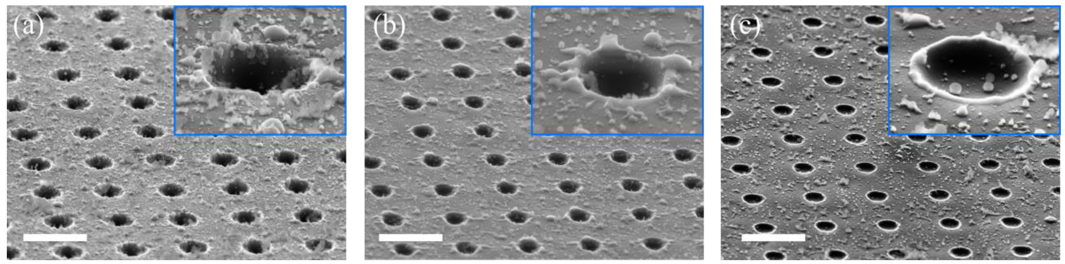
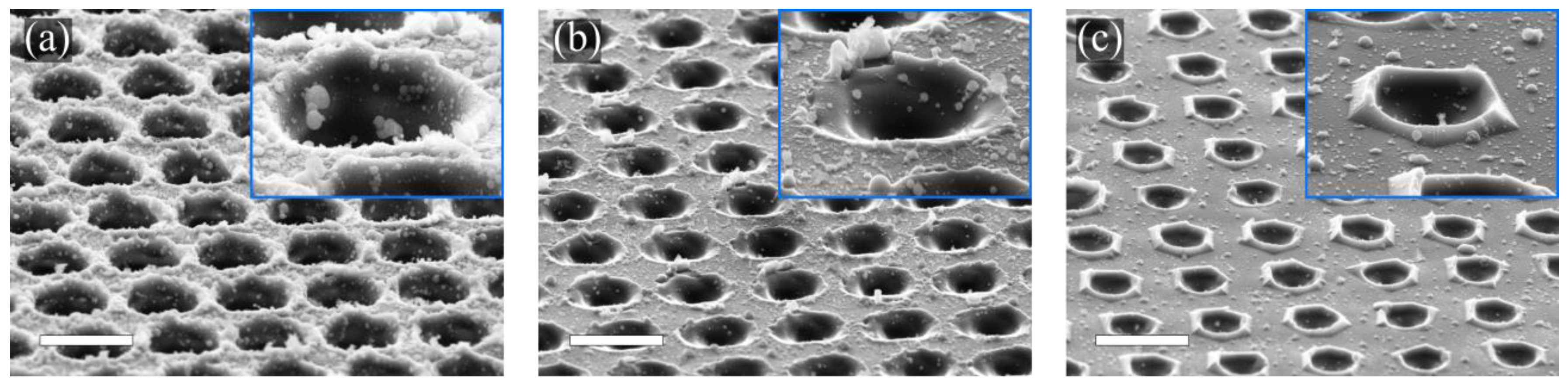
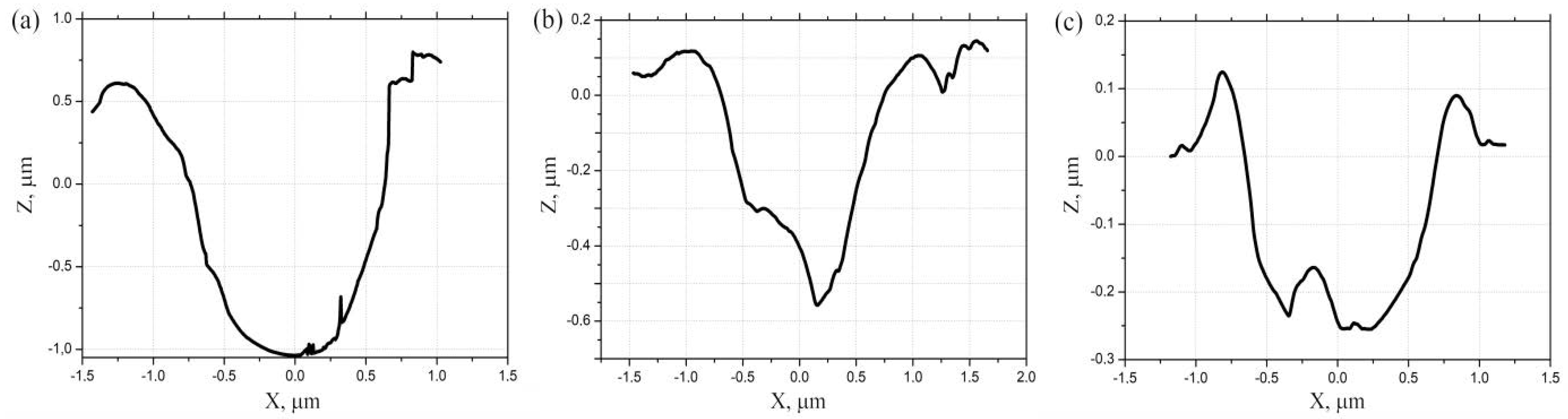
3.1. ARM Morphology

An ARM with a size of 300 × 300 μm2 was fabricated on a GaSe sample using pulses with different energies (E = 5.8, 8.4, 15.8, 23.4, 37.5 nJ). The number of pulses N was varied (N = 1, 3, 5, 8) at each energy. The ARM was fabricated only on one side of the plate. Figure 1 shows an optical image of a GaSe sample with an ARM obtained in the transmission mode. Using a scanning electron microscope, ARM morphologies at various parameters of energy and number of pulses were revealed (Figure 2).
The diameter of each element of these structures increased with increasing energy, as well as the numbers of pulses (Figure 3).
To increase the total transmission of the GaSe sample, the direct writing of ARMs on two faces was demonstrated. For this purpose, after writing 4 ARMs with E = 37.5 nJ and the number of pulses at 8, 5, 3, and 1, the sample was turned over on one side, and ARM structures were written on the other side opposite one another, with similar parameters. Images of these structures obtained using optical and electron microscopes are shown in Figure 4 and Figure 5, respectively. Surface topography profiles of a single crater were measured by an atomic force microscope (Figure 6).
The profiles along the center of a single crater inscribed at E = 37.5 nJ and pulse numbers 8, 3, 1 were obtained from 2D surface topography and presented in Figure 7. The depth of the crater increased from 0.3 μm at the impact of one pulse to 0.7 μm at impact of 3 pulses and to 1.7 μm at impact of 8 pulses. Moreover, in the case of single pulse impact, the height of the crater rim was measured, and it equaled to ≈100 nm. Thus, the increase in the number of pulses used for the creation of a single crater led to an increase in the depth of the crater, resulting in more effective antireflective spectral properties of ARM in this case.

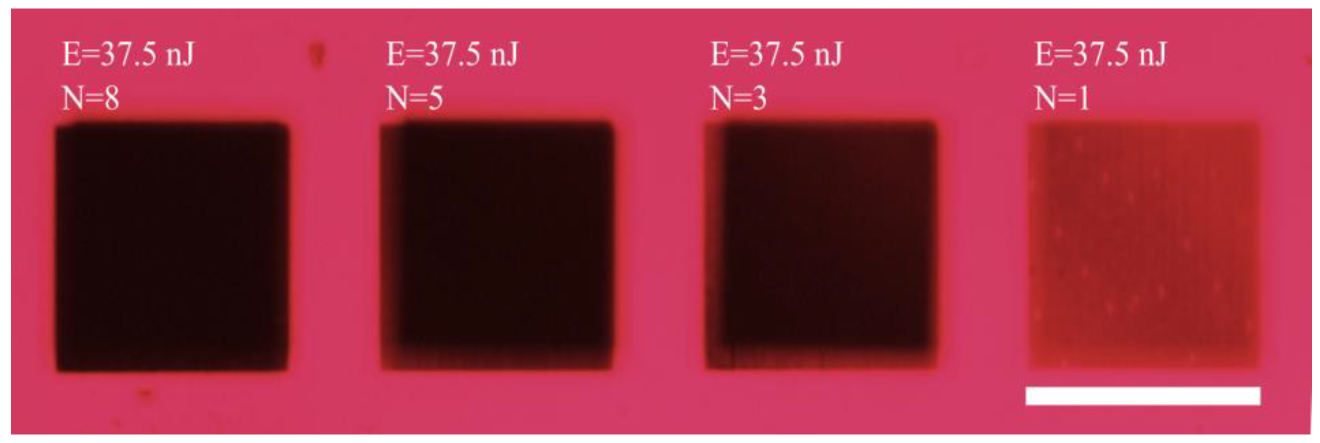
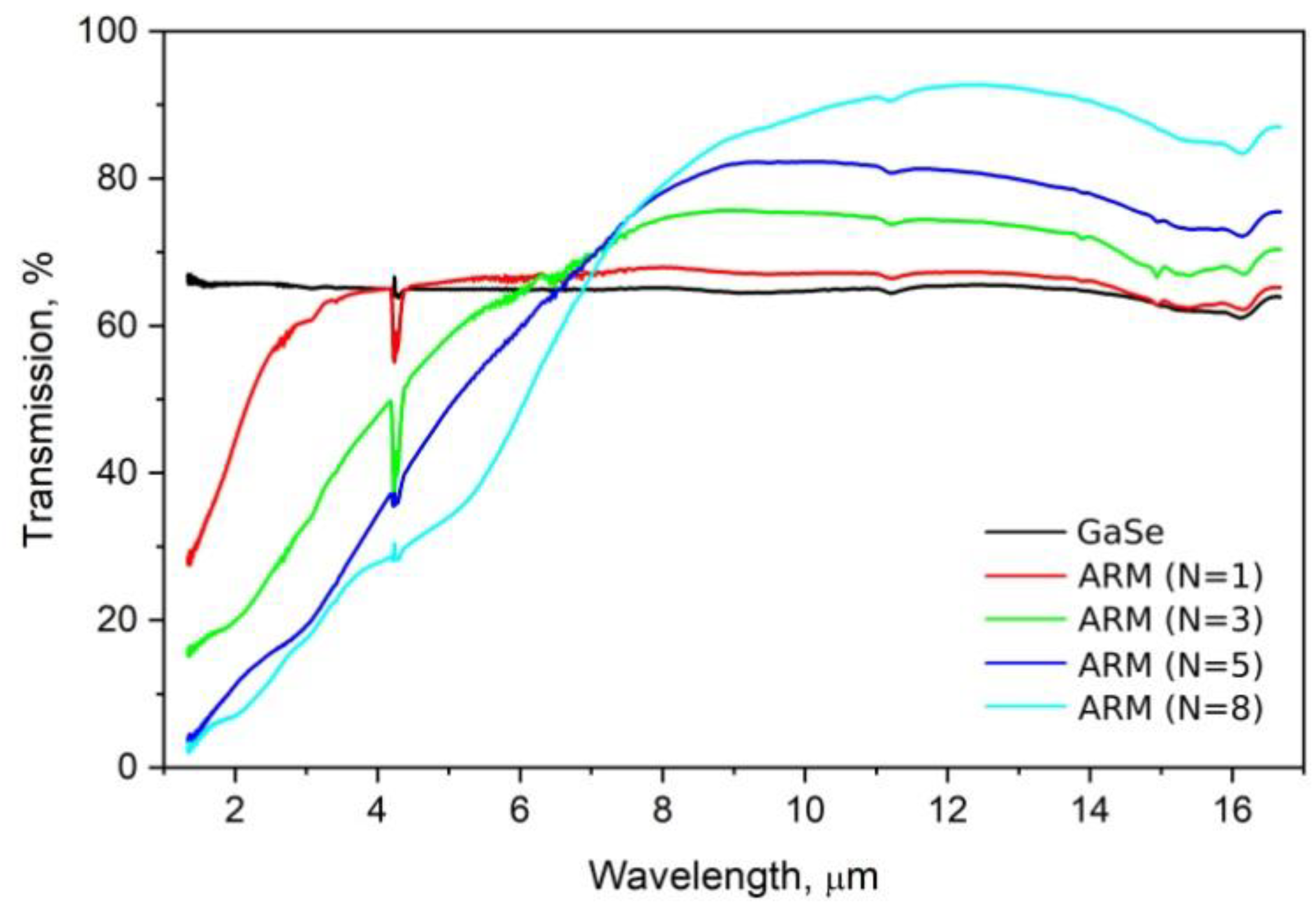
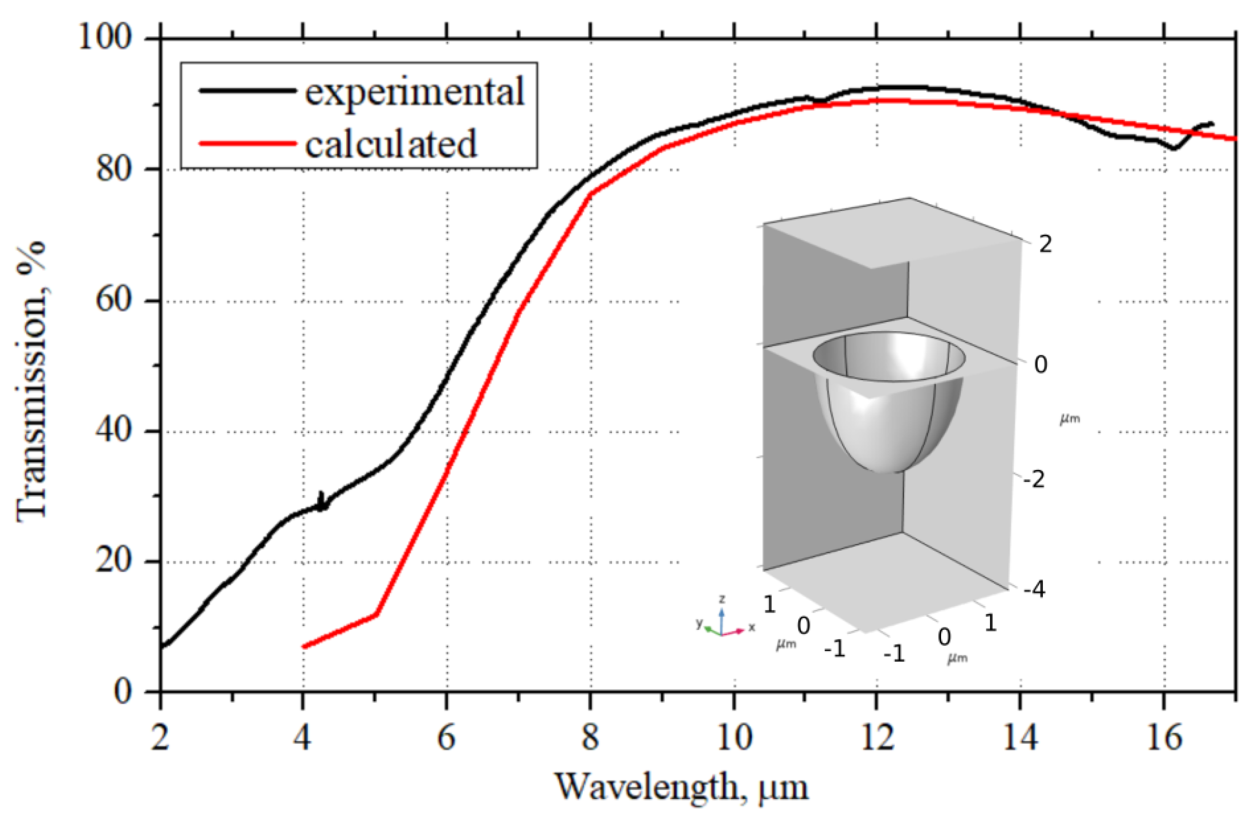
3.2. Transmission Spectra
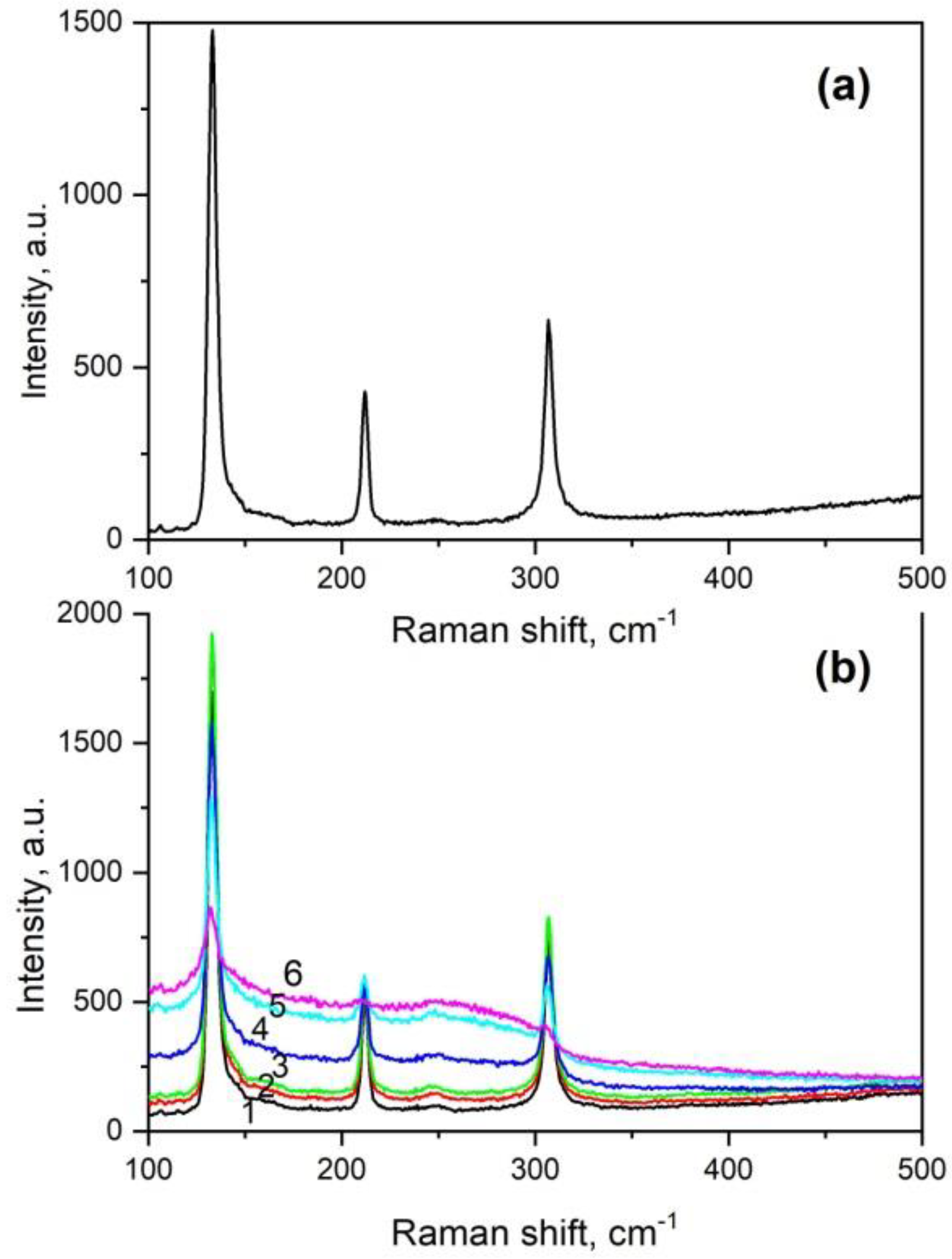
The measured transmission in the mid-IR spectral range of a freshly cleaved GaSe sample was around 65% and could be increased by an inscription of ARM. For this purpose, various ARM structures were inscribed on the GaSe sample at different pulses of energy (E = 5.8 nJ, 8.4 nJ, 15.8 nJ, and 23.4 nJ) and numbers of laser pulses used for the creation of a single crater (N = 1, 3, 5, 8). The obtained transmission spectra of ARMs are presented in Figure 8 in comparison with the initial transmission spectrum of a GaSe monocrystal (black line on the Figure 8).
It was shown that the transmission of the GaSe sample with an ARM increased with the increase of pulses of energy and numbers of pulses. The maximal increase of transmission measured at a wavelength of 10 μm from the ARM inscribed on one side of the GaSe sample was ≈10% (Figure 9a). The cross-point wavelength where the transmission of the sample was increased by ARM writing in comparison with an initial GaSe surface varied from 3.5 to 7 μm (Figure 9b) and was found to experience a red shift at higher pulses of energies E (15.8 and 23.4 nJ), from 4 to 7 μm, with the increase in the numbers of pulses. As it was shown previously in [16], an inscription of ARM on both sides of the crystal sample resulted in an enhancement of antireflection features of the ARM, and it improved by 2 times in comparison with an inscription of ARM on one side.
The maximal transmission in the mid-IR of the GaSe sample with an ARM was obtained at pulses energy of 37.5 nJ. Figure 10 shows the transmission spectra at different numbers of pulses N = 1, 3, 5, and 8, in the case of ARM inscription on both sides of the GaSe sample. Thus, at a pulse energy of 37.5 nJ and number of pulses at N = 8, the transmission increase of the ARM inscribed on one side was 15% (at wavelength of 12 µm) and 30% in the case of the ARM inscribed on both sides of the GaSe sample, resulting in a transmission of up to 94% (Table 1). Unfortunately, the maximal transmission was achieved at a certain wavelength of 12 µm, while the transmission decreased at shorter and longer wavelengths. The possibility of further increasing the transmission and shifting the crosspoint to the short wavelength was supposed to be possible by reducing the ARM period and the changing of crater shapes by using shorter laser wavelength and tight focusing conditions.

3.3. Raman Spectra

Figure 11 shows the Raman spectrum for a freshly chipped GaSe (a) crystal and for GaSe with an ARM, in the ARM region. The spectrum corresponded well to the Raman spectrum for ε-GaSe [17]. The ε-GaSe has two out-of-plane phonon modes, A11G at ~133 cm−1 and A21G at ~307 cm−1, and one in-plane E22G mode at ~212 cm−1, in line with previous reports [18]. Thus, the noncentrosymmetric polytype ε-GaSe, which has a very high χ coefficient, is predominant in grown GaSe. It can be seen that the application of an ARM on the GaSe surface led to a weakening of the intensity of narrow lines in the Raman spectrum, and the degree of attenuation increased as the energy in the pulses increased, as well as with an increase in their number from 1 to 8 (Figure 11). At the same time, a solid background appeared and intensified under the linear Raman spectrum: in the extreme case (at maximum energy per pulse), the linear spectrum completely passed into a solid background associated with an amorphous GaSe that appeared as a result of laser ablation on the surface of the GaSe crystal.

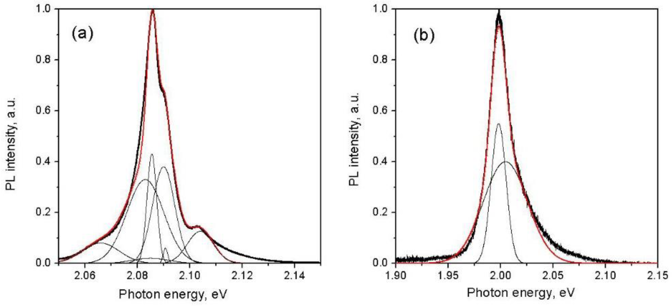
3.4. Photolumenescence Spectra

The transparency range of the ε-modification of GaSe is 0.62–20 µm [16]. The Tauc analysis for the shape of the fundamental absorption edge at 80 K gives the values of the band gap Eg = 2.11 and Eg = 2.087 eV for direct and indirect band-to-band electronic transitions [16], which is in good agreement with the results of the theoretical consideration of the GaSe energy spectrum from the first principles [19]. Since Eg is minimal for indirect band-to-band transitions, GaSe refers to indirect semiconductors, and this is consistent with the conclusions of other authors [20].
In the PL spectra of crystalline GaSe, a dominant narrow line of about 590 nm at 80 K is usually observed, which shifts to 620 nm at room temperature (a) [16]. A similar spectrum can be observed for the GaSe c ARM after laser ablation (Figure 12b), although an additional wide band with a maximum of about 750 nm appears.
Figure 13 and Figure 14 show the PL spectra obtained with a higher resolution, and the fine structure is visible here. The same Figures show the results of the decomposition of the spectra into Gaussian components; the positions of the components (eV, photon energy and nm, wavelength) are given in Table 2 and Table 3 for crystalline GaSe and in the ARM region, after ablation. Here, the lines 2.104 and 2.090 eV can be attributed to direct and indirect band-to-band electronic transitions [21]. The two narrowest components, with a value of FWHM (full width on half-maximum) at the level of several units of meV (components 4 and 5, with energies of 2.08 and 2.091 eV in Table 2) are associated in the literature with the glow of direct and indirect free excitons (DFE, IFE, respectively) [16]. Broader components with FWHM values in the range of 10–17 meV, located at lower photon energies (in the range of 2.06–2.085 eV) in the low-temperature PL spectra, bind to direct and indirect excitons associated with neutral acceptors (DBE, IBE, respectively) [20]. Broadened lines in the range of 1.9–2.06 eV, sometimes observed in the PL spectra, are attributed to the manifestation of impurity states [21]. In particular, two broad bands of 1.38 and 1.77 eV (900 and 700 nm, respectively) are caused by Mn, whereas bands of 1.6 and 1.9 eV (775, 652 nm) are characteristic of GaSe crystals activated by Cd [22]. The appearance of exciton lines and the absence of impurity bands indicate the high quality of our crystals, both in composition and structure. The shape of the spectra and the decomposition results are consistent with the results obtained earlier for the non-centrosymmetric ε-polytype GaSe [20]. In the case of the ARM, the decomposition components are significantly broadened and the FWHM values are sometimes 10 times higher, as a result of damage to the GaSe structure. As for the broad band of 750 nm in the PL spectrum for the GaSe c ARM, it may be due to the glow of amorphous selenium on the surface of GaSe after ablation. Several broad bands with maxima of 1.6, 1.8, 1.9, 2.1, and 2.3 eV are observed in thin films of amorphous selenium, of which the first and last are dominant (underlined, at wavelengths of about 750 and 540 nm) [23]. This conclusion is in good agreement with our direct observations of selenium particles on the GaSe surface using SEM [16].

3.5. Numerical Simulation

The modification profile obtained with AFM was approximated with a polynomial function of the 4th order using the curve_fit function of the SciPy package for the Python programming language. Odd coefficients were assumed to be zero, as the modifications were symmetric. Afterwards, the approximation polynomial was the following: z(x) = a x4 + bx2 + c. With coefficients a , b, and c satisfying modification profiles, the polynomial would have 4 roots: ± x 1 and ± x 2 , where x 2 > x 1 . The peculiarities of AFM profiles were excluded from the approximated data. The modification depth beyond the second root of the approximation polynomial ( x > x 2 ) was assumed to be 0.
The phenomenon was simulated using the Wave Optics module of COMSOL Multiphysics 6.0. The model geometry was the following: the upper layer of air, with thickness of 2 µm; the lower layer of GaSe, with thickness of 3 µm; the modification surface, given as the 4th order polynomial of r = x 2 + y 2 , where the depth beyond the second root of approximation polynomial ( r > r 2 ) was set to be 0. Geometry for the case of E = 37.5 nJ and N = 8 pulses is shown at Figure 15b. Wavelength-dependent refractive index for GaSe was taken from COMSOL’s material library [24], and the air was assumed to be 1. The port with the incident plane wave, polarized along the X-axis, was placed on the top surface. The corresponding receiving port was placed at the bottom surface. Perfectly matched layers were located below the GaSe layer and above the air layer to absorb the scattered field that reflected or did not match the receiving port conditions. The Floquet periodicity was set in the X and Y directions to imitate infinite structure. Simulated transmittance was squared to obtain the value for the case with modifications on both sides.
Simulation results are shown at Figure 16. They qualitatively corresponded to experimental data, depending on the number of pulses: transmittance rapidly decreased in the shortwave region and increased in the longwave region. However, transmittance for wavelengths above 7 µm was higher in the experiment than in the simulation for the corresponding number of pulses. Geometry of ablation craters did not fully define the optical property of the structure. More likely, laser pulse impacts additionally caused change to the refractive index on the crystal surface due to changes of chemical composition, for example, the formation of a thin Ga2O3 layer [16], which has a refractive index of about 1.88 [25], leading to an increase in transmittance.
Better agreement of simulation and experiment in the long-wave region shown in Figure 17 was obtained with the modification profile in the form of a semi-ellipsoid (diameter 2.5 µm, depth 2 µm). The ablated volume in this case was bigger than that obtained with AFM, which could prove the existence of a domain a with lower refractive index.

4. Conclusions

In conclusion, large single crystals of GaSe were grown by the Bridgman–Stockbarger method. Using optical spectroscopy (Raman, absorption, luminescence), the obtained GaSe crystals were attributed to a non-centrosymmetric ε modification. The appearance of free exciton lines and the absence of impurity bands in low-temperature PL spectra indicated the high quality of our crystals, both in composition and structure. Using femtosecond laser pulses of 1026 nm, with an energy in the range of 5.8–37.5 nJ and the number of pulses from 1 to 8, periodic ARMs were inscribed on the surface of the cleaved plates of a nonlinear optical crystal of GaSe. After the ARM fabricating and ablating part of the GaSe material, a solid background associated with an amorphous substance on the plate surface appeared in the Raman spectrum of GaSe. The narrow line in the low-temperature PL spectra broadened and weakened in intensity, whereas an additional broad band of about 750 nm, related to amorphous selenium, appeared. An increase in the transmission in the mid-IR from 65% to 80% for an ARM fabricated on one side and up to 94% for ARMs fabricated on both (opposite) sides was shown. The transmission increase of 29% compared to unmodified GaSe was demonstrated, which significantly exceeded the result of previous work −8% [16]. Based on surface 2D profiles of the craters in the ARMs obtained by atomic force microscopy, the transmission spectra for GaSe with ARMs were numerically calculated. A good quantitative agreement between the experimental and calculated data (spectra) was obtained under the assumption of changes in the composition of the ablated material. The obtained results on an increased transmittance of nonlinear optical crystals based on ARMs provides a route towards the development of high-power mid-IR lasers, efficient high-harmonic generators, and optoelectronic devices.

Author Contributions

Conceptualization, L.I., A.D. and A.Y.; methodology, A.D. and A.Y.; software, A.S. (Andrey Simanchuk); formal analysis, A.S. (Andrey Simanchuk); investigation, A.Y., A.D., S.L., V.F., V.S. and A.S. (Alexander Shklyaev); writing—A.Y., A.D. and V.S.; original draft preparation, A.D.; writing—review and editing, A.D., L.I. and A.Y.; funding acquisition, L.I. and S.B. All authors have read and agreed to the published version of the manuscript.

Funding

This research was funded by the Russian Science Foundation, grant number 20-72-10027 (crystal growth, spectroscopic investigations) and partly performed on state assignment of IGM SB RAS (composition, chemical analysis) and state assignment/budget of IAE SB RAS (femtosecond writing).

Institutional Review Board Statement

Not applicable.

Informed Consent Statement

Not applicable.

Data Availability Statement

The data presented in this study are available upon request from the corresponding author.

Acknowledgments

The work was carried out using the equipment of the Center for Collective Use “Spectroscopy and Optics” of the IA and E SB RAS. The SEM studies were performed on the equipment of CKP «VTAN» (ATRC) of the NSU Physics Department.

Conflicts of Interest

The authors declare no conflict of interest.

References

  1. Nikogosyan, D. Nonlinear Optical Crystals: A Complete Survey; Springer: New York, NY, USA, 2005; ISBN 0-387-22022-4. [Google Scholar]
  2. Voevodin, V.G.; Voevodina, O.V.; Bereznaya, S.A.; Korotchenko, Z.V.; Morozov, A.N.; Sarkisov, S.Y.; Fernelius, N.C.; Goldstein, J.T. Large single crystals of gallium selenide: Growing, doping by In and characterization. Opt. Mater. 2004, 26, 495–499. [Google Scholar] [CrossRef]
  3. Singh, N.B.; Suhre, D.R.; Balakrishna, V.; Marable, M.; Meyer, R.; Fernelius, N.; Hopkins, F.K.; Zelmon, D. Far-infrared conversion materials: Gallium selenide for far-infrared conversion applications. Prog. Cryst. Growth Charact. Mater. 1998, 37, 47–102. [Google Scholar] [CrossRef]
  4. Wang, T.; Li, J.; Zhao, Q.; Yin, Z.; Zhang, Y.; Chen, B.; Xie, Y.; Jie, W. High-quality GaSe single crystal grown by the Bridgman method. Materials 2018, 11, 186. [Google Scholar] [CrossRef] [PubMed] [Green Version]
  5. Late, D.J.; Liu, B.; Luo, J.; Yan, A.; Matte, H.S.S.R.; Grayson, M.; Rao, C.N.R.; Dravid, V.P. GaS and GaSe ultrathin layer transistors. Adv. Mater. 2012, 24, 3549–3554. [Google Scholar] [CrossRef] [PubMed]
  6. Shigetomi, S.; Ikari, T. Electrical and photovoltaic properties of Cu-doped p-GaSe/n-InSe heterojunction. J. Appl. Phys. 2000, 88, 1520–1524. [Google Scholar] [CrossRef]
  7. Bernier, G.; Jandl, S.; Provencher, R. Spontaneous and stimulated photoluminescence of GaSe in the energy range 2.075–2.125 eV. J. Lumin. 1986, 35, 289–300. [Google Scholar] [CrossRef]
  8. Basov, N.G.; Bogdankevich, O.V.; Pechenov, A.N.; Abdullaev, G.B.; Akhundov, G.A.; Salaev, E.Y. Stimulated emission in a GaSe single crystal when excited by fast electrons. Sov. Phys. Dokl. 1965, 10, 329–333. [Google Scholar]
  9. Hulliger, F. Structural Chemistry of Layer-Type Phases; Lévy, F., Ed.; Springer: Dordrecht, The Netherlands, 1976; ISBN 978-94-010-1148-8. [Google Scholar]
  10. Maschke, K.; Levy, F. New Series, Group III: Crystal and Solid State Physics; Springer: Berlin/Heidelberg, Germany, 1983. [Google Scholar]
  11. Chattopadhyay, S.; Huang, Y.F.; Jen, Y.J.; Ganguly, A.; Chen, K.H.; Chen, L.C. Anti-reflecting and photonic nanostructures. Mater. Sci. Eng. R Rep. 2010, 69, 1–35. [Google Scholar] [CrossRef]
  12. Choy, T.C. Effective Medium Theory: Principles and Applications; Oxford University Press: Oxford, UK, 2015; ISBN 9780198705093. [Google Scholar]
  13. Rayleigh, L. On Reflection of Vibrations at the Confines of two Media between which the Transition is Gradual. Proc. Lond. Math. Soc. 1879, s1-11, 51–56. [Google Scholar] [CrossRef]
  14. Bushunov, A.A.; Tarabrin, M.K.; Lazarev, V.A. Review of Surface Modification Technologies for Mid-Infrared Antireflection Microstructures Fabrication. Laser Photonics Rev. 2021, 15, 2000202. [Google Scholar] [CrossRef]
  15. Bushunov, A.A.; Teslenko, A.A.; Tarabrin, M.K.; Lazarev, V.A.; Isaenko, L.I.; Eliseev, A.P.; Lobanov, S.I. Fabrication of antireflection microstructures on the surface of GaSe crystal by single-pulse femtosecond laser ablation. Opt. Lett. 2020, 45, 5994. [Google Scholar] [CrossRef] [PubMed]
  16. Yelisseyev, A.P.; Isaenko, L.I.; Lobanov, S.I.; Dostovalov, A.V.; Bushunov, A.A.; Tarabrin, M.K.; Teslenko, A.A.; Lazarev, V.A.; Shklyaev, A.A.; Babin, S.A.; et al. Effect of antireflection microstructures on the optical properties of GaSe. Opt. Mater. Express 2022, 12, 1593. [Google Scholar] [CrossRef]
  17. Beechem, T.E.; Kowalski, B.M.; Brumbach, M.T.; McDonald, A.E.; Spataru, C.D.; Howell, S.W.; Ohta, T.; Pask, J.A.; Kalugin, N.G. Oxidation of ultrathin GaSe. Appl. Phys. Lett. 2015, 107, 173103. [Google Scholar] [CrossRef]
  18. Hoff, R.M.; Irwin, J.C. Raman scattering in GaSe. Phys. Rev. B 1974, 10, 3464–3470. [Google Scholar] [CrossRef]
  19. Schlüter, M. The electronic structure of GaSe. Nuovo Cim. 1973, 13, 313–360. [Google Scholar] [CrossRef]
  20. Depeursinge, Y. Electronic properties of the layer III-VI semiconductors. A comparative study. Nuovo Cim. 1981, 64, 111–150. [Google Scholar] [CrossRef]
  21. Aulich, E.; Brebner, J.L.; Mooser, E. Indirect Energy Gap in GaSe and GaS. Phys. Stat. Sol. B 1969, 31, 129–131. [Google Scholar] [CrossRef]
  22. Tagiev, B.G.; Niftiev, G.M.; Abushov, S.A. Photoluminescence of GaSe: Mn Single Crystals. Phys. Stat. Sol. B 1984, 121, K195–K199. [Google Scholar] [CrossRef]
  23. Cingolani, A.; Evangelisti, F.; Minafra, A.; Rizzo, A. Photoluminescence of GaSe. Phys. Stat. Sol. A 1973, 17, 449–454. [Google Scholar]
  24. Kato, K.; Tanno, F.; Umemura, N. Sellmeier and thermo-optic dispersion formulas for GaSe (Revisited). Appl. Opt. 2013, 52, 2325. [Google Scholar] [CrossRef]
  25. Rebien, M.; Henrion, W.; Hong, M.; Mannaerts, J.P.; Fleischer, M. Optical properties of gallium oxide thin films. Appl. Phys. Lett. 2002, 81, 250–252. [Google Scholar] [CrossRef]
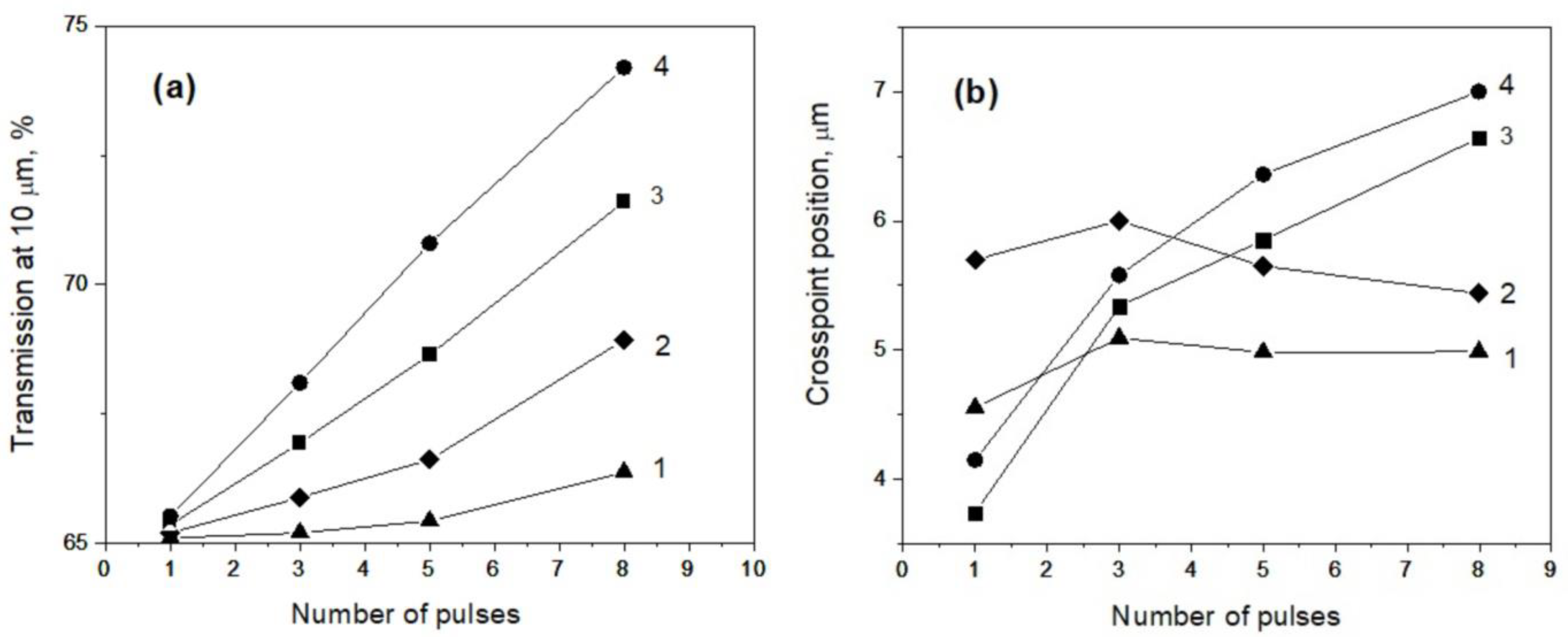
Figure 1. Optical image of GaSe surface with an ARM, inscribed at E = 8.4, 15.8 and 23.4 nJ (bottom, middle, and top row consequently), and numbers of pulses: N = 1, 3, 5, and 8. The scale bar has a length of 300 µm.
Photonics 09 00774 g001
Figure 2. SEM image of GaSe surface with an ARM, inscribed at E = 8.4 nJ and numbers of pulses: 8 (a), 3 (b), 1 (c). Scale bar—3 μm. One of the craters is shown separately in the upper right corner of each image.
Photonics 09 00774 g002
Figure 3. Dependence of crater diameter on pulses of energy E = 5.8, 8.4, 15.8, and 23.4 nJ and numbers of pulses N= 1, 3, 5, 8. For each energy, four diameter values corresponding to pulse numbers N = 1, 3, 5, and 8 are given (from bottom to top).
Photonics 09 00774 g003
Figure 4. Optical image of the GaSe surface with ARMs, inscribed at E = 37.5 nJ and numbers of pulses N = 1, 3, 5, and 8 on both sides of the sample.
Photonics 09 00774 g004
Figure 5. SEM image of GaSe surface with ARMs, inscribed at E = 37.5 nJ and numbers of pulses: 8 (a), 3 (b), and 1 (c). Scale bar—3 μm. One of the craters is shown separately in the upper right corner of each image.
Photonics 09 00774 g005
Figure 6. Surface topography of a single crater inscribed at E = 37.5 nJ and numbers of pulses: 8 (a), 3 (b), and 1 (c). Scale bar−1 μm.
Photonics 09 00774 g006
Figure 7. Surface profiles of a single crater inscribed at E = 37.5 nJ and numbers of pulses: 8 (a), 3 (b), and 1 (c).
Photonics 09 00774 g007
Figure 8. Transmission spectra of an ARM inscribed on one side of a GaSe sample at: E = 5.8 nJ (a), 8.4 nJ (b), 15.8 nJ (c), and 23.4 nJ (d). Single crater of an ARM was obtained by impacts of 1, 3, 5, and 8 laser pulses. The transmission spectrum of the initial GaSe sample is shown by a black line for comparison.
Photonics 09 00774 g008
Figure 9. (a) The transmission at a wavelength of 10 μm for GaSe with ARMs inscribed at different pulses of energies: 5.8 nJ (1), 8.4 nJ (2), 15.8 nJ (3), and 23.4 nJ (4) and numbers of pulses: 1, 3, 5, and 8. (b) The cross-point wavelength in the transmission spectra of the initial GaSe and GaSe with ARMs inscribed at the same experimental parameters.
Photonics 09 00774 g009
Figure 10. Transmission spectra of the ARM inscribed on both sides of the GaSe sample at E = 37.5 nJ. Single crater of the ARM was obtained by impact of 1, 3, 5, and 8 laser pulses. The transmission spectrum of the initial GaSe sample is shown by a black line for a comparison.
Photonics 09 00774 g010
Figure 11. Raman spectra for single crystal GaSe (a) and from the surface of GaSe with an ARM (b), obtained at an excitation of 532 nm, with the following parameters (pulse energy and number of pulses): 5.8 nJ/N = 1; 5.8nJ/N = 8; 8.4nJ/N = 8; 15.8 nJ/N = 8; 23.4 nJ/N = 8; and 37.5 nJ/N = 8 (curves 1−6, respectively).
Photonics 09 00774 g011
Figure 12. PL spectra for GaSe (a) and GaSe with an ARM (b) measured at 300 K (red line) and 80 K (black line) at 532 nm excitation. (c) The dependence of the intensity of the main PL line (at T = 80 K) on the parameters of laser pulses (energy per pulse and the number of pulses for the creation of one crater in an ARM at GaSe).
Photonics 09 00774 g012
Figure 13. PL spectra for the GaSe crystal obtained at an excitation of 532 nm, at 80 K (a) and 300 K (b). Thick black lines show the experimentally measured PL spectrum, thin black lines show the Gaussian components, and a thick red line shows the sum of these components.
Photonics 09 00774 g013
Figure 14. PL spectra for a GaSe crystal with an ARM obtained at an excitation of 532 nm, at 80 K (a) and 300 K (b). Thick black lines show the experimentally measured PL spectrum, thin black lines show the Gaussian components, and a thick red line shows the sum of these components.
Photonics 09 00774 g014
Figure 15. (a) AFM profiles of ARM craters inscribed with an energy of 37.5 nJ and a different number of pulses (solid) and 4th order approximations (dashed). Semi−ellipsoidal modification assumption for 8 pulses (green); (b) the model’s geometry: upper layer−air, lower layer−GaSe.
Photonics 09 00774 g015
Figure 16. Transmittance spectra of crystal with modification on both sides: experimental data of the spectra of ARMs inscribed on both sides at E = 37.5 nJ and different pulse numbers (solid) and simulation (dashed with squares).
Photonics 09 00774 g016
Figure 17. Transmission spectra of a GaSe crystal with ARMs on both sides: experimental data for 8 pulses, E = 37.5 nJ nJ (solid), and simulation (dashed with squares), with the modified profile of a crater in the form of a semi-ellipsoid.
Photonics 09 00774 g017
Table 1. Cross-point wavelengths and transmission of the ARM inscribed at E = 37.5 nJ on the both sides of the GaSe sample.
Number of Pulses, NCross-Point Wavelength, μmTransmission at 10.6 μm, %Maximal Transmission,% (at Wavelength), µm
14.3568.269.0 (8.03)
36.0276.176.8 (8.92)
56.5183.383.5 (9.5)
86.9091.794.1 (12.3)
Table 2. The result of decomposition into Gaussian components for the PL line in the GaSe crystal.
T = 80 K
NNEg, eVWavelength, nmFWHM, meV
12.066599.9516
22.083595.017
32.085594.517
42.0855594.34
52.0907592.72.5
62.090593.110
72.104589.112
T = 300 K
NN Eg, eV Wavelength, nm FWHM, meV
11.998620.418
22.0045618.351
Table 3. The result of decomposition into Gaussian components for the PL line in the GaSe crystal with an ARM.
T = 80 K
NNEg, eVWavelength, nmFWHM, meV
11.951635171
22.033609.630
32.073597.937
42.086594.212
52.101589.918
T = 300 K
NN Eg, eV Wavelength, nm FWHM, meV
11.658747.6175
21.833676.293
31.981625.747
Publisher’s Note: MDPI stays neutral with regard to jurisdictional claims in published maps and institutional affiliations.

