Article

Electrochemical Redox In-Situ Welding of Silver Nanowire Films with High Transparency and Conductivity

1
College of Materials Science and Engineering, Zhejiang University of Technology, Hangzhou 310014, China
2
College of Environment, Zhejiang University of Technology, Hangzhou 310014, China
*
Authors to whom correspondence should be addressed.
Submission received: 11 May 2022 / Revised: 23 June 2022 / Accepted: 27 June 2022 / Published: 30 June 2022
(This article belongs to the Special Issue Metal Nanomaterials as Efficient Electrocatalysts)

Abstract

:
Silver nanowire (AgNW) networks with high transparency and conductivity are crucial to developing transparent conductive films (TCFs) for flexible optoelectronic devices. However, AgNW-based TCFs still suffer from the high contact resistance of AgNW junctions with both the in-plane and out-of-plane charge transport barrier. Herein, we report a rapid and green electrochemical redox strategy to in-situ weld AgNW networks for the enhanced conductivity and mechanical durability of TCFs with constant transparency. The welded TCFs show a marked decrease of the sheet resistance (reduced to 45.5% of initial values on average) with high transmittance of 97.02% at 550 nm (deducting the background of substrates). The electrochemical welding treatment enables the removal of the residual polyvinylpyrrolidone layer and the in-situ formation of Ag solder in the oxidation and reduction processes, respectively. Furthermore, local conductivity studies confirm the improvement of both the in-plane and the out-of-plane charge transport by conductive atomic force microscopy. This proposed electrochemical redox method provides new insights on the welding of AgNW-based TCFs with high transparency and low resistance for the development of next-generation flexible optoelectronic devices. Furthermore, such conductive films based on the interconnected AgNW networks can be acted as an ideal supporter to construct heterogeneous structures with other functional materials for wide applications in photocatalysis and electrocatalysis.

1. Introduction

With the expanding demand in the field of transparent and flexible electronics, transparent conductive films (TCFs) have attracted enormous attention as one of the most indispensable components in many advanced flexible optoelectronic devices [1,2,3,4,5,6,7]. Indium tin oxide (ITO), the most commonly used transparent conductive material, struggles to meet the requirements of next-generation TCFs due to its brittle properties and its expensive cost due to the scarcity of indium [8,9,10]. Therefore, great efforts have been devoted to developing various nanomaterials, such as graphene, carbon nanotubes, metal nanowires and conductive polymers, for replacing the conventional ITO [11,12,13,14,15,16,17]. Among them, silver nanowires (AgNWs) have been considered one of the most promising candidates owing to their high optical transparency, low sheet resistance and excellent mechanical flexibility [16]. Nowadays, due to their high flexibility and optoelectronic features, AgNWs have been widely used for applications in touch-screen displays [18,19], flexible fuel cells [20,21,22], stretchable energy devices [23,24,25], transparent sensors [26,27], and air filters [28,29].
Currently, the fabrication of TCFs based on AgNWs contains two primary solution-based synthesis and coating processes: (1) the synthesis of uniform AgNWs using the polyol-reduction method in the presence of polyvinylpyrrolidone (PVP) [30,31,32,33]; (2) the fixation of pre-synthesized AgNWs on a flexible and transparent substrate by multiple coating techniques such as spin-/dip-/bar-coating and spraying [34]. The above solution-based processes are facile, low-cost and easy-to-operate; however, AgNW-based TCFs (AgNW-TCFs) still suffer from many issues to meet commercial applications. One of the main issues is the high contact resistance of AgNW junctions, where both the in-plane and out-of-plane charge transport barrier is formed due to the nanoscale gap between nanowires with weak bonding and the insulating layer of the residual PVP on the surface of AgNWs [35,36,37]. Several post-treatment strategies have been proposed to weld the junctions of AgNW networks by applying heat [38,39], pressure [40,41], intense pulsed light (IPL) [42,43,44,45], laser [46,47,48], electricity [49], capillary force [50,51], composite method [52,53,54], and chemical reactions [55,56,57], enabling the removal of the insulating PVP layer, the formation of additional solder at the junctions, and the improved contact between nanowires.
For example, heat-induced welding, mechanical welding, and light-induced welding have been reported and carried out to markedly reduce the high junction resistance. However, flexible polymer substrates with a low glass transition temperature and plastic character may be damaged under the thermal annealing and mechanical stress processes, respectively. Light-induced plasmonic welding depends on high optical power density, which limits the large-scale fabrication of TCFs for commercial application. These strategies are mainly to achieve the welding of AgNW networks through physical processes. In addition to the physical welding, the chemical reduction welding, based on a solution-based process by applying additional additives in joints to weld the AgNWs, is also an effective method to improve the conductivity of networks [55,56,57,58,59]. Especially, homogeneous Ag chemically/electrochemically reduced from Ag+ is an ideal soldering material to weld adjacent nanowires [60,61]. The Ag solder can be deposited on the surface of AgNW networks by an electroplating technique, which is widely applied in the industrial roll-to-roll process with an applied potential and an electrolyte containing Ag+. However, most studies have focused on improving the in-plane or out-of-plane charge transport solely through these welding methods. Consider both the in-plane and out-of-plane charge transport not only can effectively reduce the sheet resistance but also can improve the current collection efficiency of TCFs-based devices [36].
Therefore, the simultaneous removal of the PVP layer and solder formation is an effective way to achieve the improvement of the in-plane and out-of-plane charge transport. Herein, we demonstrate an in-situ welding strategy to improve the charge transport of AgNW-TCFs without the influence of their transmittance by the electrochemical redox reactions. The as-prepared TCFs, composed of cross-aligned AgNWs coated on a polyethyleneterephthalate (PET) substrate, are selected to be conducted the electrochemical redox welding investigation under a three-electrode system in a neutral electrolyte containing NaClO4 and NaCl (Scheme 1). The electrochemical welding treatment includes oxidation and reduction steps to remove the residual PVP layer and form AgCl as the solder precursor, as well as to in-situ generate the Ag solder from AgCl, respectively. The welded TCFs with a constant transmittance show a significant decrease in resistance, which is attributed to the improved in-plane and out-of-plane charge transport properties of AgNW networks.

2. Materials and Methods

2.1. Materials

AgNO3 (AR), CuCl2 (AR), PVP (K-30, 55,000) and PVP (K-90, 360,000) were purchased from Sigma-Aldrich. ε-PLL (AR) was donated from Aladdin Reagent Co. Ltd. (Shanghai, China) NaCl (AR), NaClO4 (AR), ethylene glycol (AR) and ethanol (AR) were obtained from Sinopharm Chemical Reagent Co., Ltd. (Shanghai, China) Polyethylene terephthalate (PET, 125 μm) were purchased from Kangdexin Composite Materials Group (Suzhou, China). All materials were used as received without further purification. Ultrapure water (18.2 MΩ·cm) was produced using an ultrapure water system (GWB-1).

2.2. Synthesis of AgNWs

AgNWs were synthesized by a polyol reduction method as in previous reports [30,31]. In this method, PVP, AgNO3, CuCl2 and ethylene glycol were introduced as the structure-directing and stabilizing agent, the silver source, the heterogeneous nucleation site and the solvent and reducing agent, respectively. Typically, 115 mL ethylene glycol, 0.421 g PVP (K30) and 0.406 g PVP (K90) were added into a three-neck flask, which was placed in a heating jacket with the temperature set to 140 °C. Meanwhile, 0.825 mmol L−1 CuCl2 and 45 mmol L−1 AgNO3 ethylene glycol solutions were prepared, followed by dropwise adding 3.2 mL CuCl2 solution and 20 mL AgNO3 solution when the temperature reached 140 °C. Thereafter, the reaction lasted for 50 min and then the flask was removed to a water bath until the solution completely cooled to room temperature. Finally, a centrifugal purification method was employed to remove the impurities such as organic matter, silver nanoparticles and short rods. The purified AgNWs were dispersed in ethanol to obtain AgNW ink for further use.

2.3. Fabrication of AgNW-TCFs

PET was cut into 10 cm × 10 cm and then exposed to ultraviolet ozone for 30 min. The as-prepared AgNW ink was diluted to 3.5 mg mL−1, and ε-PLL was dissolved in ultrapure water and then configure to a concentration of 0.1%. In order to obtain the orthogonal network, AgNW films were fabricated firstly by spin coating the ε-PLL solution (40 μL) on a clean PET substrate, followed by bar-coating the AgNW ink (300 μL) in an automatic film applicator, with the speed of 50 mm s−1. After that, orthogonal AgNW-TCFs were obtained by rotating the films 90° and repeating the bar-coating step [62].

2.4. Electrochemical Welding of AgNW-TCFs

The electrolyte was prepared by mixing NaClO4 (0.5 mol L−1) and NaCl (0.1 mol L−1) to obtain homogeneous solutions. For all electrochemical reactions, a platinum wire and an Ag/AgCl electrode were used as the counter electrode and the reference electrode, respectively. The AgNW-TCFs as the working electrode were oxidized at 0.3 V (vs. Ag/AgCl) and then reduced at −0.15 V (vs. Ag/AgCl) in an N2-saturated 150 mL electrolyte for 50 s and 100 s, respectively. Finally, the welded AgNW-TCFs were removed immediately after reaction, followed by rinsing in ultrapure water and drying in N2 flow.

2.5. Conductive Atomic Force Microscopy Studies

2.5.1. Topographical Imaging

A nanoIR2 AFM-IR instrument equipped with the contact mode NIR2 probe (Anasys Instruments, Inc., Santa Barbara, CA, USA) was used to obtain the atomic force microscopy (AFM) topographical images of AgNW-TCFs, AgNW-TCFs-Ox and AgNW-TCFs-Re. The scan rate was set at 0.5 Hz, the scan range was selected as 1 μm × 1 μm, and the x and y resolution are both 300 points. The AFM topographical images of AgNW-TCFs were collected and analyzed by the Analysis Studio software (Version 3.15, Anasys Instrument Inc.)

2.5.2. Nanoscale Electrical Analysis

The localized electrical analysis of AgNW-TCFs was carried out using the nanoIR2 AFM-IR instrument to operate in a conduction mode. A conductive AFM probe (PR-EX-CAFM-5) (Anasys Instruments Inc., USA) was adopted for data collection. The topography and conductivity of the sample can be obtained simultaneously by one scan at a bias voltage of 0.052 V. Pointwise spectroscopy can be obtained by sweeping and measuring corresponding current in a bias range.

2.6. Characterization

The morphology of samples was characterized by scanning electron microscopy (SEM, Nova Nano 450). The alignment of silver nanowires arrays was examined by optical microscope (OM, Zeiss). The morphology and lattice constant of silver nanowires were observed by transmission electron microscopy (TEM, Talos S-FEG). The phase analysis was determined by X-ray diffraction (XRD, DX-27mini). The binding energy of elements was characterized by X-ray photoelectron spectroscopy (XPS, Kratos AXIS Ultra DLD). The sheet resistance of AgNW-TCFs were measured by four-point probes resistivity measurement system (RTS-9). Optical transmittance spectra of AgNW-TCFs were measured by using UV−vis−NIR spectrophotometer (Lambda 750). Cyclic voltammetry (CV), linear sweep voltammetry (LSV), electrochemical impedance spectroscopy (EIS) and chronoamperometry curves were recorded on a CHI660E electrochemical workstation. LSV were carried out with a scan rate of 10 mV s−1. EIS curves were obtained at a bias of 0.15 V (vs. Ag/AgCl) in the frequency range of 100 kHz to 0.01 Hz. Current-voltage responses for AgNW-TCFs were monitored by an interconnected system of a digital source-meter (Keithley 2450) with an input voltage of 0.1 V and a real time tensile testing machine (Instron 5966).

3. Results and Discussion

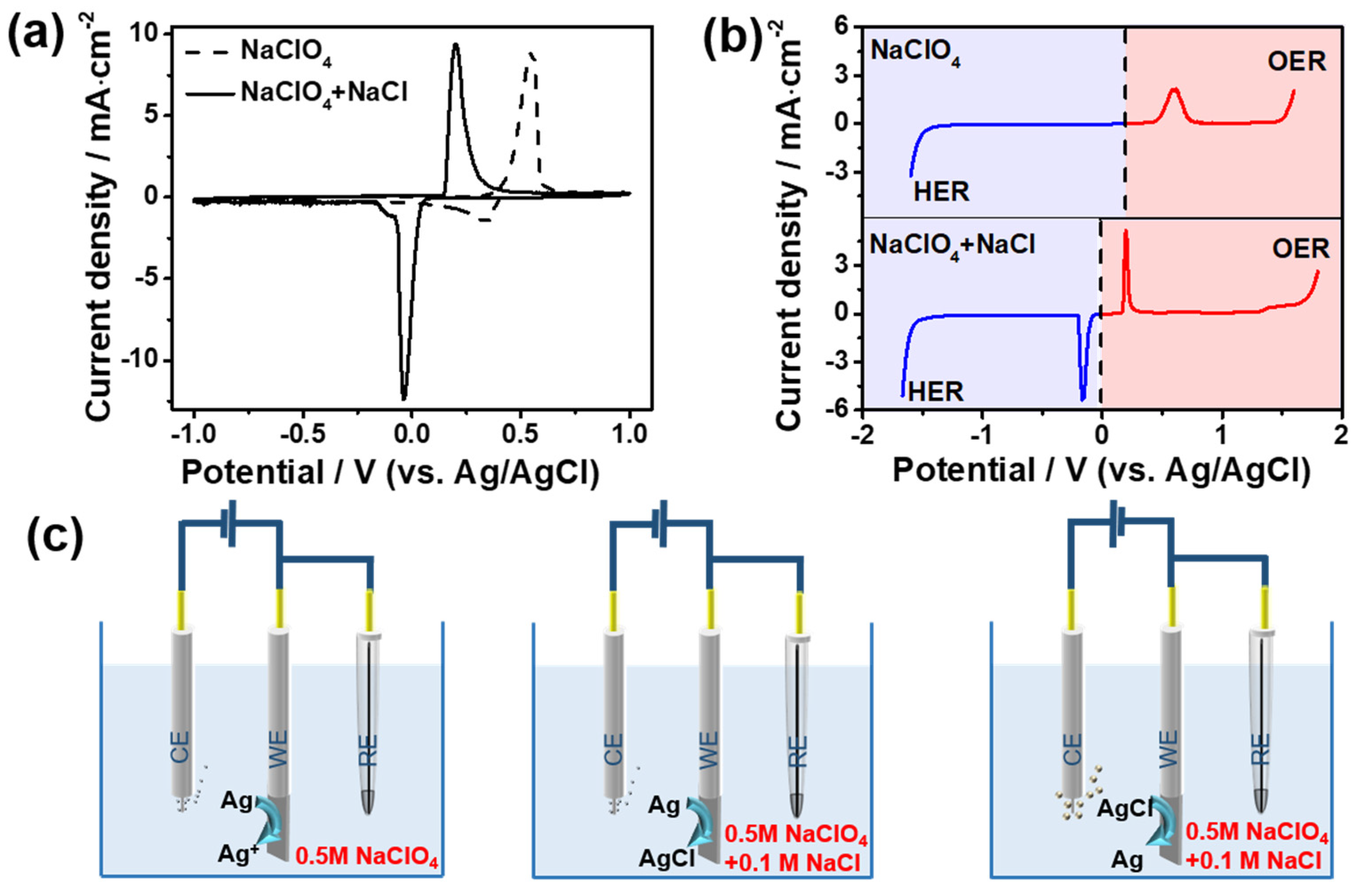
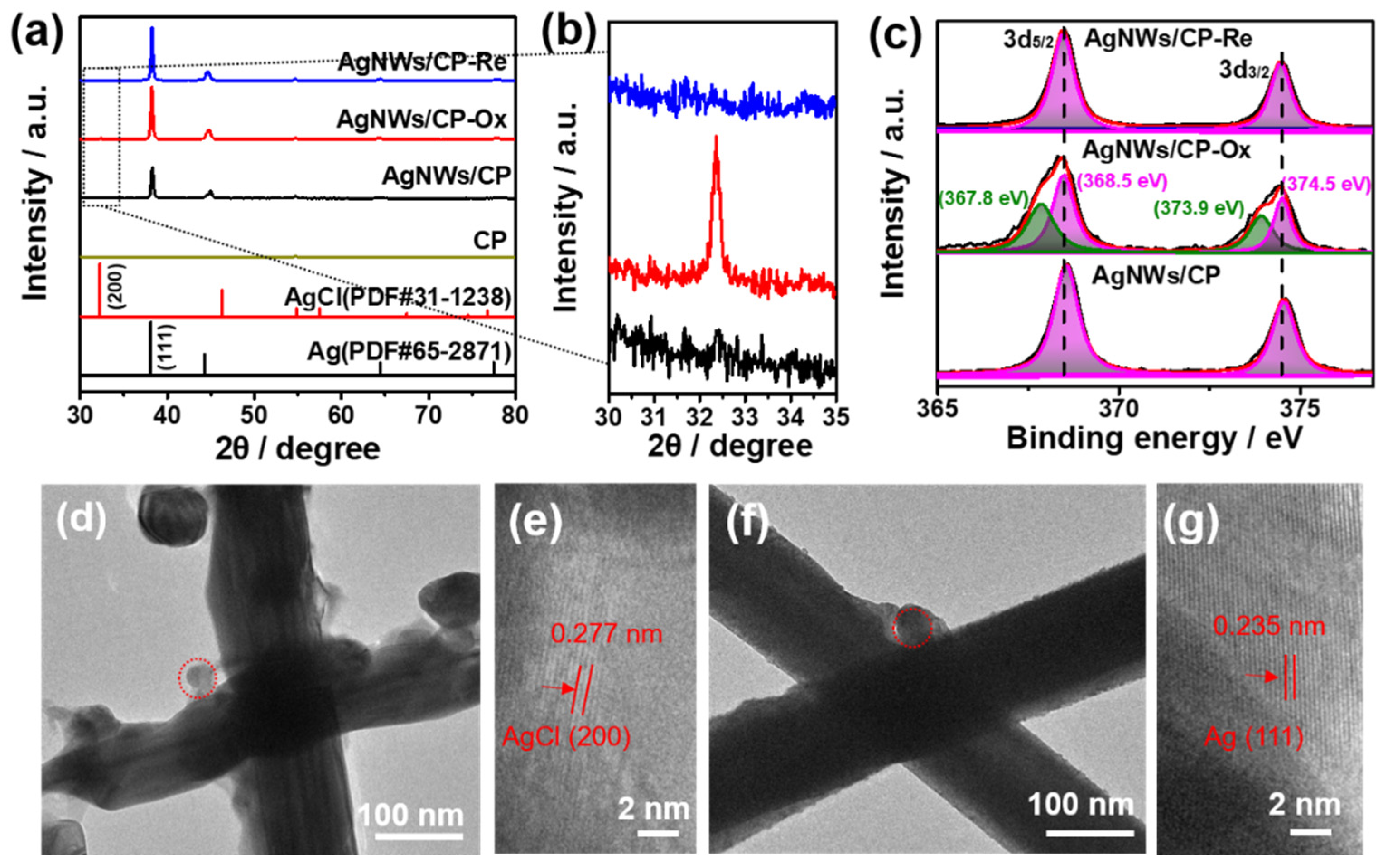
3.1. Characterization and Electrochemical Analysis of AgNWs

The conventional polyol reduction method was employed to prepare AgNWs with diameters of 99 ± 19 nm and lengths of 35 ± 10 μm, which were determined by the scanning electron microscopy (SEM) and optical microscopy images, respectively (Figure S1). The FoM (Figure-of-merit) of AgNW-TCFs is 227, and the haze is 3.2% [63]. The electrochemical behavior of AgNWs was carefully studied using a three-electrode system with the as-prepared AgNW ink supported on a glass carbon electrode (GCE) as a working electrode. Figure 1a shows cyclic voltammetry (CV) profiles of AgNWs using a scan window from −1 to 1 V versus (vs.) an Ag/AgCl reference electrode at a scan rate of 100 mV s−1 in a N2-saturated 0.5 M NaClO4 aqueous solution with and without NaCl. A couple of redox peaks can be observed at 0.55 V and 0.34 V (vs. Ag/AgCl) in the NaClO4 electrolyte without NaCl during the positive and reverse potential sweeps, which are attributed to the electrochemical oxidation of Ag to form Ag+ ions and the subsequent reduction of Ag+, respectively [64]. Note that the area of the reduction peak is much lower than that of the oxidation peak, and the redox peaks sharply decrease until disappear after multiple CV scanning (Figure S2a). This phenomenon can be explained by the diffusion of Ag+ ions into the solution, while only a small amount of Ag+ around the electrode (in the compact layer) can be reduced to Ag until AgNWs on the GCE are completely consumed. In the presence of NaCl, the oxidation and reduction peaks of AgNWs negatively shifted to 0.2 and −0.04 V (vs. Ag/AgCl), respectively (Figure 1a) [65]. Meanwhile, the redox peaks with similar area remain stable after multiple CV scanning (Figure S2b), suggesting that partial Ag on the surface of AgNWs can be reversibly oxidized and reduced owing to the formation of AgCl.
Figure 1b shows liner sweep voltammetry (LSV) curves of AgNWs in the absence and presence of Cl with a scan rate of 10 mV s−1. Without the addition of NaCl, the anodic current density is contributed by the oxidation of AgNWs to form Ag+ at 0.6 V (vs. Ag/AgCl) and the oxygen evolution reaction (OER) at 1.42 V (vs. Ag/AgCl), while the cathodic current density is only contributed by the hydrogen evolution reaction (HER) at −1.29 V (vs. Ag/AgCl) [66]. In contrast, a pronounced peak located at −0.16 V (vs. Ag/AgCl) is attributed to the reduction of AgCl in the cathodic current after adding NaCl. The schematic diagrams in Figure 1c show the oxidation processes on the working electrode in the electrolyte with and without NaCl as well as the reduction process in the electrolyte with NaCl.
To further understand the electrochemical conversion of AgNWs, we conducted SEM, X-ray diffraction (XRD) and X-ray photoelectron spectroscopy (XPS) measurements for investigating the morphology, crystal structure and valence state of pristine, oxidated and reduced AgNWs, respectively (Figure 2a–c, Figures S3 and S4). AgNW ink was first loaded on a carbon paper substrate (AgNWs/CP) by a drop-casting method. The AgNWs/CP samples were oxidated at 0.3 V (vs. Ag/AgCl) and then reduced at −0.15 V (vs. Ag/AgCl) in a 0.5 M NaClO4 electrolyte containing 0.1 M NaCl. The nanoscale solder can be observed on the surface of AgNWs especially at junctions in SEM images (Figure S3). Figure 2a shows the XRD patterns of all samples and the standard patterns of Ag ang AgCl. For the pristine AgNWs/CP, the peaks located at 38.2°, 44.2°, 64.4°, and 77.5° are assigned to the (111), (200), (220) and (311) planes of the Ag phase. After electrochemical oxidation, the XRD pattern of AgNWs/CP-Ox shows a characteristic peak at 32.5° attributed to the formation of AgCl (Figure 2b). The peak disappears in the XRD pattern of AgNWs/CP-Re, indicating that the formed AgCl can be completely converted into Ag after electrochemical reduction. In addition, the high-resolution XPS spectra of all samples show two typical peaks at 368.5 and 374.5 eV (Figure 2c), which are assigned at Ag 3d5/2 and 3d3/2, respectively. Meanwhile, the additional peaks at 367.8 and 373.9 eV in the spectrum of AgNWs/CP-Ox imply the presence of Ag+. Furthermore, the slight shift of the binding energy of Ag3d5/2 and 3d3/2 may be attributed to the removal of residual PVP during the electrochemical oxidation process [36].
For transmission electron microscopy (TEM) and high-resolution TEM (HRTEM) studies, AgNWs were loaded on a gold grid to in situ electrochemically oxidate and reduce under the same welding conditions. TEM images show that a pristine AgNW is coated by a clear PVP layer with the thickness of ~4 nm (Figure S5a), which disappeared after the electrochemical oxidation process. As shown in Figure S5b and Figure 2d, the formation of nanolayer and nanoparticles on the surface of AgNWs can be observed in TEM images. The HRTEM image of a nanoparticle highlighted by red cycle in Figure 2d shows the existence of the lattice fringes, in which is in agreement with the (200) interplanar spacing of AgCl (Figure 2e). After being further electrochemical reduced, AgNWs are welded by the formation of Ag solder confirmed by TEM and HRTEM images (Figure 2f,g), in which the lattice spacing is ~0.235 nm assigned to the (111) interplanar spacing of Ag.
The above results suggest that the reversible electrochemical conversion of Ag can achieve the removal of the PVP layer on the surface of AgNWs and the formation of the nanoscale Ag solders at junctions of AgNWs. Therefore, it is expected to weld AgNW-TCFs with the improved in-plane and out-of-plane charge transport properties by using such in situ electrochemical redox process.

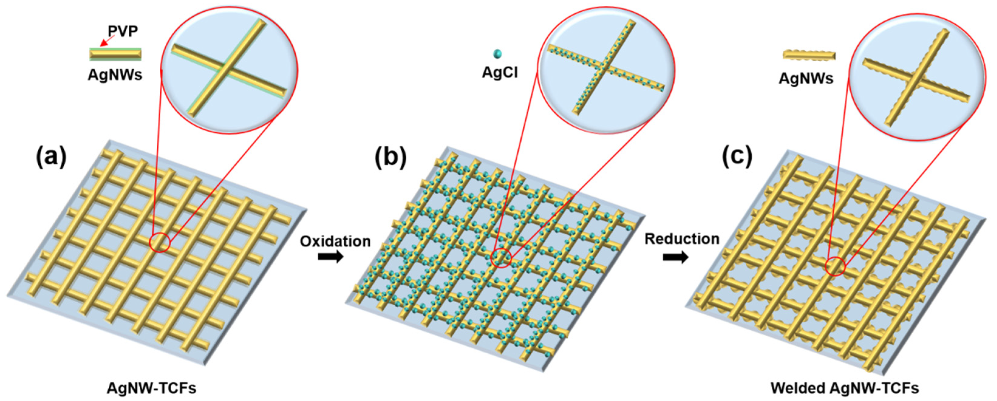
3.2. Fabrication of Cross-Aligned AgNW Network Films

The conventional polyol reduction method was employed to prepare AgNWs with diameters of ~99 nm and lengths of ~35 μm, which were determined by the scanning electron microscopy (SEM) and optical microscopy images, respectively (Figure S1). The electrochemical behavior of AgNWs was carefully studied using a three-electrode system with the as-prepared AgNW ink supported on a glass carbon electrode (GCE) as a working electrode. Figure 1a shows cyclic voltammetry (CV) profiles of AgNWs using a scan window from −1 to 1 V versus (vs.) an Ag/AgCl reference electrode at a scan rate of 100 mV s−1 in a N2-saturated 0.5 M NaClO4 aqueous solution with and without NaCl. A couple of redox peaks can be observed at 0.55 V and 0.34 V (vs. Ag/AgCl) in the NaClO4 electrolyte without NaCl during the positive and reverse potential sweeps, which are attributed to the electrochemical oxidation.

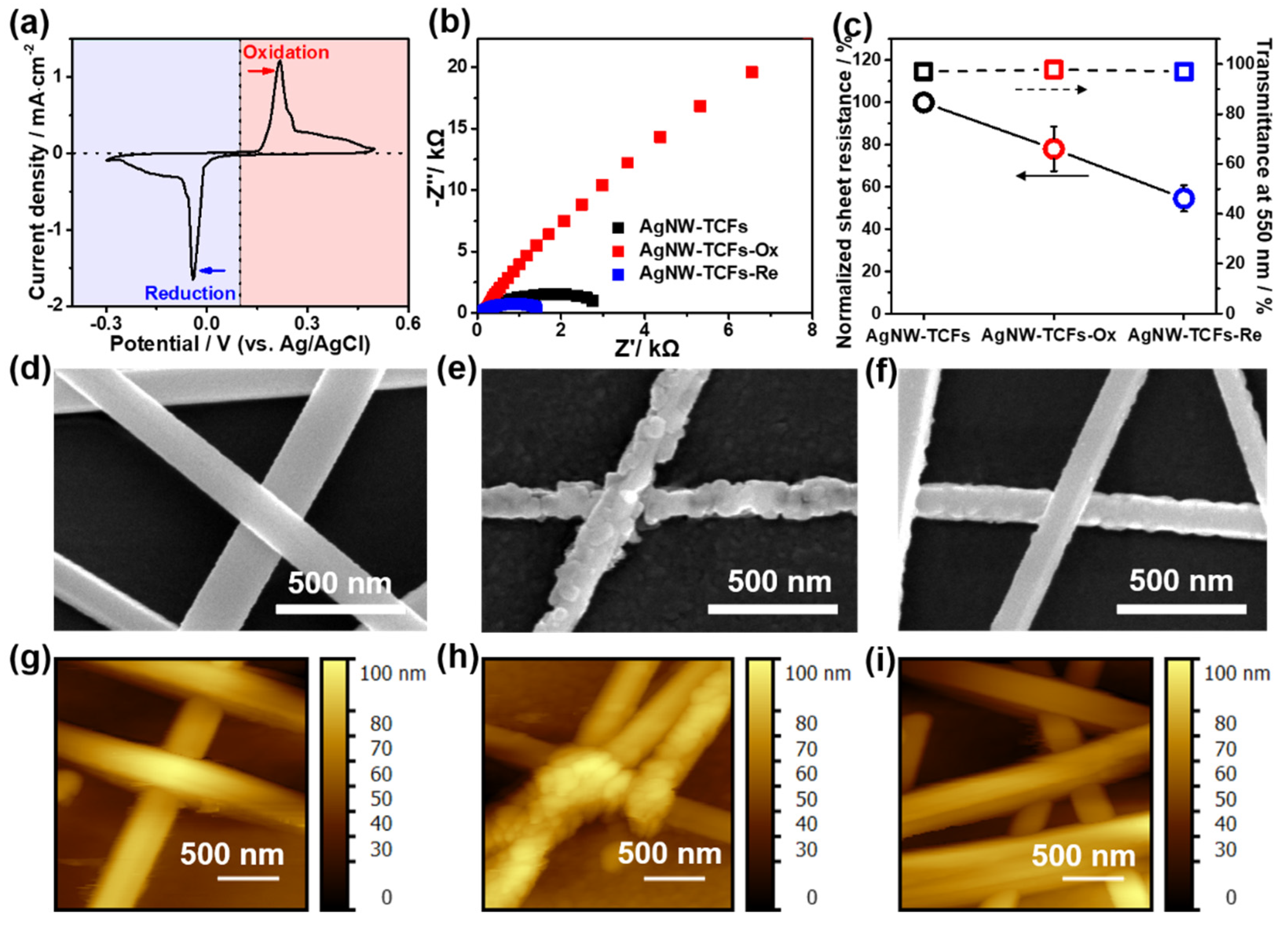
3.3. Electrochemical Redox Welding Process

As shown in Figure 3a, the CV profile of AgNW-TCFs shows a couple of typical redox peaks, which is consistent with that of AgNWs on GCE. In a typical electrochemical welding process, the pristine AgNW-TCFs were oxidized at 0.3 V (vs. Ag/AgCl) for 50 s to obtain the intermediate AgNW-TCFs-Ox and were subsequently reduced at −0.15 V (vs. Ag/AgCl) for 100 s to achieve the welded AgNW-TCFs-Re. The change of current density was contributed by the redox reactions of Ag in the chronoamperometry curves (Figure S8), indicating the rapid electrochemical processes and different amounts of AgCl formed at different oxidation potentials. Noted that the oxidation potential at 0.3 V (vs. Ag/AgCl) was optimized based on the morphology evolution of AgNWs (Figures S9–S11). There could be a galvanic replacement to destroy the AgNWs under a high reaction potential (>0.5 V), as shown in Figure S11. However, when the potential in an appropriate reaction potential (0.3 V), AgCl nanoparticles are uniformly attached to the surface of AgNWs without damaging the overall structure of AgNWs (Figure S10). Electrochemical impedance spectroscopy (EIS) measurements were carried out to reveal the out-of-plane charge transfer behavior of AgNW-TCFs, AgNW-TCFs-Ox and AgNW-TCFs-Re. Figure 3b shows Nyquist plots with semicircles for AgNW-TCFs and AgNW-TCFs-Re as well as with a Warburg line for AgNW-TCFs-Ox. The smaller diameter of the semicircle for AgNW-TCFs-Re relative to AgNW-TCFs suggests a great improvement in the out-of-plane charge transfer after electrochemical redox treatment [36]. This is attributed to the removal of the PVP layer and the welded junctions between AgNWs.

3.4. Optical and Morphological Analysis

The optical properties of AgNW-TCFs, AgNW-TCFs-Ox, and AgNW-TCFs-Re were further investigated and their transmittances were estimated to be around 97.02% at 550 nm deducting the background of PET substrates (Figure 3c and Figure S12). The FoM (Figure-of-merit) and the haze of AgNW-TCFs is 227 and 3.2%, respectively [66]. The negligible effect on optical transmittance manifests such electrochemical redox welding treatment is a mild process without affecting the overall structure of AgNW-TCFs, which is further confirmed by SEM and atomic force microscopy (AFM) images. Figure 3d–i show the morphology evolution of AgNWs during the electrochemical redox welding process, showing a slight charge on the surface of AgNWs. During the welding process, Ag atoms on the surface of AgNWs are oxidized to form an AgCl nanolayer and nanoparticles that enlarge the contact surface between nanowires under the positive current, whereafter AgCl can be reduced to in situ form nanoscale Ag solders and weld the nanowires under the negative current.

3.5. Sheet Resistance Analysis

To prove the improvement of the electrical conductivity of AgNW-TCFs-Re after welding, the sheet resistance of AgNW-TCFs, AgNW-TCFs-Ox, and AgNW-TCFs-Re were evaluated by a four-point probe resistivity measurement system. The sheet resistance data of representative samples is listed in Table S1, and the comparison of normalized sheet resistance for AgNW-TCFs before and after welding is shown in Figure 3c and Figure S13. Compared with the pristine AgNW-TCFs, AgNW-TCFs-Ox exhibits reduced sheet resistance after the electrochemical oxidation treatment. This phenomenon is attributed to the removal of the PVP layer and the improvement of in-plane charge transport properties of AgNW networks, which is in agreement with the results of TEM and XPS, as well as being further confirmed by following local conductivity studies. The further-reduced sheet resistance of AgNW-TCFs-Re indicates the AgNW networks welded by the formed Ag solders during the reduction process and the further improvement of in-plane charge transport properties of the AgNW networks. The statistical results show that the sheet resistance of AgNW-TCFs-Re can be reduced by 45.5% on average after the electrochemical welding process. The sheet resistance of AgNW-TCFs-Re is 53.99 ± 8.13 Ω/sq (Figure S13), and the nonuniformity factor (NUF) is 13.47% [67].

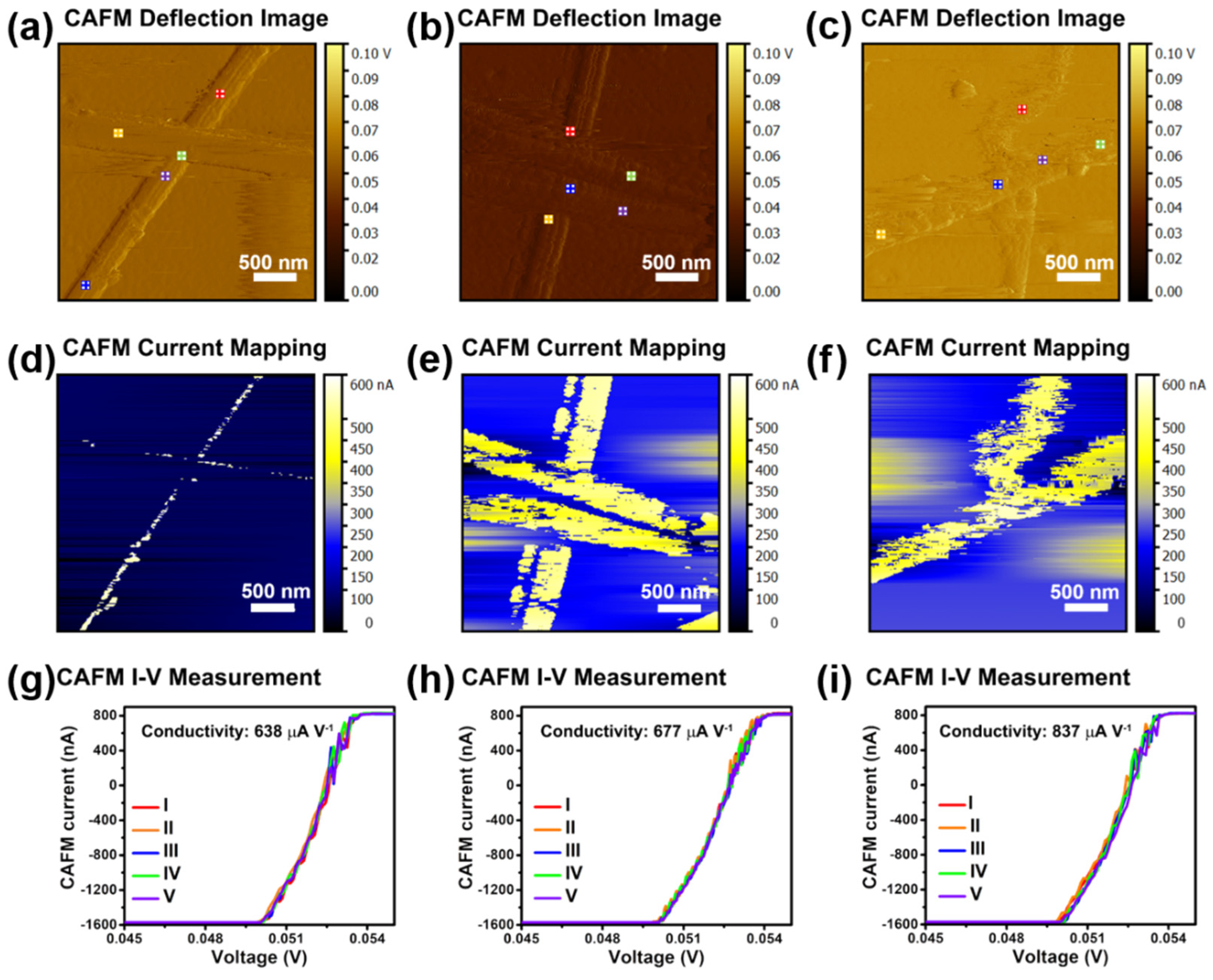
3.6. Local Conductivity Analysis

To further explore the effect of microstructure on the conductivity of macroscopic materials, the conductive AFM (CAFM) technique was employed to evaluate local conductivity of different samples during welding. CAFM is an effective method to map local current distribution with sensitivity up to picoamperes, and obtain local current–voltage (I-V) curves at a single point or even a series of points on a map [68,69]. Hence, it is suitable for comparing the local electrical properties of not only composite structures with different electrical conductivity in a single map but also materials in different maps with the same setting parameters.
The CAFM deflection images of two AgNWs crossing each other in pristine AgNW-TCFs, intermediate AgNW-TCFs-Ox and welded AgNW-TCFs-Re are shown in Figure 4a, Figure 4b and Figure 4c, respectively. The results are consistent with those obtained from the SEM and AFM images. Noted that the surface of welded AgNWs is prone to scratching on contact with the probe under the same bias voltage (0.052 V) and scan rate (0.5 Hz), which may be due to the tolerance of soft and rough surfaces decreases under the same current densities and friction after electrochemical welding. This phenomenon also evidences that Ag is reduced from AgCl adhered to the surface of AgNWs, which is just the cornerstone of electrochemical welding. Figure 4d–f shows the corresponding local CAFM current distribution mapping, in which AgNW-TCFs-Ox and AgNW-TCFs-Re exhibit the similar excellent local electrical conductivity but pristine AgNW-TCFs shows a weak current mapping, which is attributed to the presence of the PVP layer blocking the current transport. This is direct evidence to show the removal of the insulating PVP layer and the improvement of the out-of-plane charge transport properties after the electrochemical oxidation treatment. Furthermore, the CAFM I-V measurements were quantitatively confirmed, meaning that the electrochemical oxidation and reduction process are both beneficial to improve the local conductivity of AgNWs. Five data points in a CAFM deflection image were selected to analyze electrical properties of single site in each sample. The linearity curves of sweep output in CAFM I-V measurements are plotted in Figure 4g–i, and the slopes of the corresponding I–V curves are calculated in Table S2. The local conductivity of each material is the same at different selected points, indicating that the conductivity of a material is consistent in different microstructure. The average local conductivity of AgNW-TCFs, AgNW-TCFs-Ox and AgNW-TCFs-Re is estimated to be 638, 677, 837 μA V−1, respectively. This indicates the improvement of the in-plane charge transport properties, which is consistent with the results of sheet resistance measurements. Overall, the local CAFM studies clearly confirm the improvement of both the in-plane and the out-of-plane charge transport after the electrochemical redox welding processes.

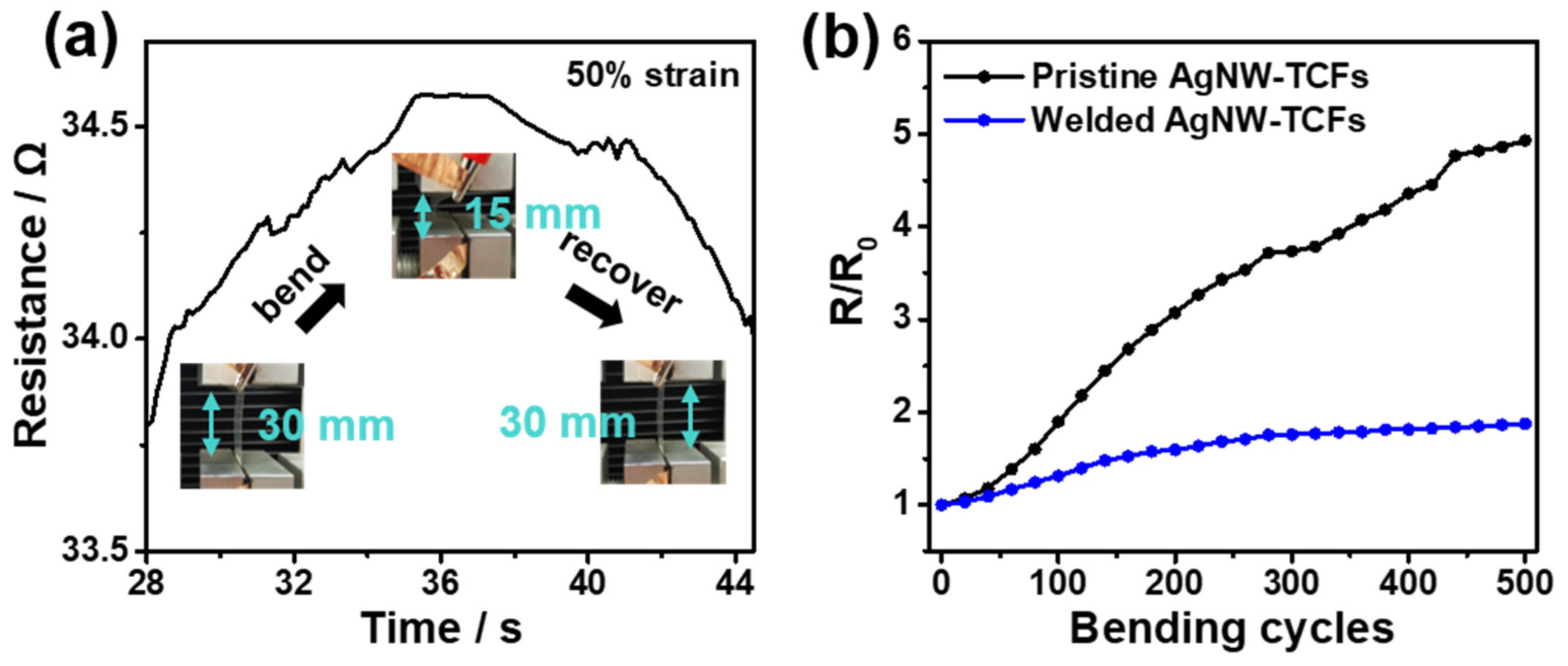
3.7. Mechanical Flexibility Stability Studies

Flexibility and stretchability are the most important factors to evaluate the mechanical stability of AgNW-TCFs [70,71,72,73,74,75]. For elastic substrate, AgNW-TCFs would be stretched to test the change of sheet resistance. For non-elastic substrate, AgNW-TCFs would be bended to evaluate the variation of sheet resistance. To further demonstrate the advantages of welded AgNW networks for practical applications, we evaluated the mechanical flexibility of the pristine and welded AgNW-TCFs by bending test. The film samples with a long strip-like shape were bent and recovered in a strain range of 0–50%, and showed an apparent resistance fluctuation recorded by interconnecting a mechanical stretching system with a supply control system. As shown in Figure 5a, the electrical resistance of AgNW-TCFs after bending reaches ~34.5 Ω from the original resistance of ~33.5 Ω. The increased resistance is due to the reduced conductive paths in the AgNW networks, affecting the electron transport and thus increasing resistance. After recovering, a slight increase in resistance is due to the presence of unrecovered paths. It is expected that the welded AgNW networks can resist the movement of nanowires during the bending process. Figure 5b shows the relative resistance variation for the pristine and welded AgNW-TCFs during 500 cycles at 50% strain. The curve of pristine AgNW-TCFs exhibits a rapid increase of relative resistance. In contrast, the curve of welded AgNW-TCFs slowly rises and a plateau emerges after 280 cycles. The relative resistance of welded AgNW-TCFs increases 1.8-fold after bending tests, which is far lower than that of pristine AgNW-TCFs (more than 4.9-fold). The time-dependent resistance studies confirm the small variation of welded AgNW-TCFs in each bending cycle (Figures S14 and S15). Therefore, the above results indicate the excellent mechanical bending stability of AgNW-TCFs after the electrochemical redox welding treatment.

4. Conclusions

In summary, we developed a rapid and green electrochemical redox strategy for welding AgNW network films in a neutral electrolyte containing NaCl. After the electrochemical redox welding, the AgNW-TCFs retain a constant transmittance of 97.02% at 550 nm (deducting the background of PET substrates) and show a marked decrease of sheet resistance (reduced to 45.5% of initial values on average). Morphological and structural characterization confirms the removal of the residual PVP layer in the electrochemical oxidation process and the formation of Ag nanoscale solder at junctions in the electrochemical reduction process. Meanwhile, local conductivity measurements and electrochemical charge transfer studies further reveal the local and whole enhancement of the in-plane and out-of-plane charge transport properties. Furthermore, the mechanical flexibility investigation shows that the change of sheet resistance of as-welded AgNW-TCFs is marked lower than that of pristine AgNW-TCFs after a 500-cycle bending test, confirming the successful welding of AgNW networks in such a facile, green and fast electrochemical redox manner. Consequently, the electrochemical redox welding strategy proposed here, aimed to fabricate AgNW-based conductive films with high transparency and low resistance, would benefit for the development of next-generation TCFs for future flexible optoelectronic devices. Furthermore, such conductive films based on the interconnected AgNW networks can act as an ideal supporter to construct heterogeneous structures with other functional materials for wide applications in photocatalysis and electrocatalysis.

Supplementary Materials

The following supporting information can be downloaded at: https://0-www-mdpi-com.brum.beds.ac.uk/article/10.3390/inorganics10070092/s1, Figure S1: SEM and optical microscope images of AgNWs; Figure S2:CV curves of AgNWs with a scan rate of 100 mV s-1 in a N2-saturated 0.5 M NaClO4 without and with 0.1 M NaCl; Figure S3: SEM images of AgNWs/CP-Ox and AgNWs/CP-Re; Figure S4: XPS survey spectra of AgNWs/CP, AgNWs/CP-Ox and AgNWs/CP-Re; Figure S5: TEM images of pristine AgNWs and oxidated AgNWs; Figure S6: Schematic illustration of the fabrication of cross-aligned AgNW-TCFs; Figure S7: Optical microscope image of a cross-aligned AgNW-TCF. Inset is the fast Fourier transform analyses, showing the orientation and uniformity of the aligned AgNWs; Figure S8: Polarization curves of AgNW-TCFs under different oxidation potentials at 0.15 V, 0.3 V and 0.5 V (vs. Ag/AgCl) for 50 s and the same reduction potential at −0.15 V (vs. Ag/AgCl) for 100 s; Figure S9: SEM images of AgNW-TCFs oxidated at 0.15 V (vs. Ag/AgCl) (a,b) and reduced at −0.15 V (vs. Ag/AgCl); Figure S10: SEM images of AgNW-TCFs oxidated at 0.3 V (vs. Ag/AgCl) (a,b) and reduced at −0.15 V (vs. Ag/AgCl); Figure S11: SEM images of AgNW-TCFs oxidated at 0.5 V (vs. Ag/AgCl) (a,b) and reduced at −0.15 V (vs. Ag/AgCl); Figure S12: UV−vis spectra and optical photographs of AgNW-TCFs, AgNW-TCFs-Ox and AgNW-TCFs-Re; Figure S13: Normalized sheet resistance of AgNW-TCFs, AgNW-TCFs-Ox and AgNW-TCFs-Re for comparing; The frequency distribution histogram of sheet resistance for AgNW-TCFs-Re; Figure S14: Time-dependent resistance variation for the pristine and welded AgNW-TCFs; Figure S15: Plots of relative resistance variation (R/R0) as a function of time for the pristine and welded AgNW-TCFs; Table S1: Comparing of sheet resistance for AgNW-TCFs, AgNW-TCFs-Ox and AgNW-TCFs-Re; Table S2: Electrical properties at five data points in a CAFM deflection image of AgNW-TCFs, AgNW-TCFs-Ox and AgNW-TCFs-Re.

Author Contributions

Methodology, W.Z., J.B. and P.Z.; formal analysis, X.P.; investigation, W.Z.; resources, C.X.; data curation, J.B., C.X., P.Z. and R.L.; writing—original draft preparation, W.Z. and J.B.; writing—review and editing, W.Z. and R.L.; supervision, W.Z.; project administration, W.Z. and R.L.; funding acquisition, W.Z. and R.L. All authors have read and agreed to the published version of the manuscript.

Funding

This research was funded by [National Natural Science Foundation of China] grant number [22105170 and 22075248] and [Natural Science Foundation of Zhejiang Province] grant number [LQ21B010001].

Institutional Review Board Statement

Not applicable.

Informed Consent Statement

Not applicable.

Data Availability Statement

Data available in a publicly accessible repository.

Conflicts of Interest

The authors declare no conflict of interest.

References

  1. Yu, L.; Shearer, C.; Shapter, J. Recent Development of Carbon Nanotube Transparent Conductive Films. Chem. Rev. 2016, 116, 13413–13453. [Google Scholar] [CrossRef] [PubMed]
  2. Cai, G.; Wang, J.; Lee, P.S. Next-Generation Multifunctional Electrochromic Devices. Acc. Chem. Res. 2016, 49, 1469–1476. [Google Scholar] [CrossRef] [PubMed]
  3. Li, D.; Lai, W.-Y.; Zhang, Y.-Z.; Huang, W. Printable Transparent Conductive Films for Flexible Electronics. Adv. Mater. 2018, 30, 1704738. [Google Scholar] [CrossRef]
  4. Wang, D.; Zhang, Y.; Lu, X.; Ma, Z.; Xie, C.; Zheng, Z. Chemical Formation of Soft Metal Electrodes for Flexible and Wearable Electronics. Chem. Soc. Rev. 2018, 47, 4611–4641. [Google Scholar] [CrossRef]
  5. Ma, Y.J.; Zhi, L.J. Graphene-Based Transparent Conductive Films: Material Systems, Preparation and Applications. Small Methods 2019, 3, 1800199. [Google Scholar] [CrossRef] [Green Version]
  6. Wang, C.; Xia, K.; Wang, H.; Liang, X.; Yin, Z.; Zhang, Y. Advanced Carbon for Flexible and Wearable Electronics. Adv. Mater. 2019, 31, 1801072. [Google Scholar] [CrossRef]
  7. Song, J.; Lee, H.; Jeong, E.G.; Choi, K.C.; Yoo, S. Organic Light-Emitting Diodes: Pushing toward the Limits and Beyond. Adv. Mater. 2020, 32, 1907539. [Google Scholar] [CrossRef]
  8. Zheng, Q.; Li, Z.; Yang, J.; Kim, J.-K. Graphene Oxide-Based Transparent Conductive Films. Prog. Mater. Sci. 2014, 64, 200–247. [Google Scholar] [CrossRef]
  9. Li, Y.; Xu, G.; Cui, C.; Li, Y. Flexible and Semitransparent Organic Solar Cells. Adv. Energy Mater. 2018, 8, 1701791. [Google Scholar] [CrossRef]
  10. Qiu, T.; Luo, B.; Akinoglu, E.M.; Yun, J.-H.; Gentle, I.R.; Wang, L. Trilayer Nanomesh Films with Tunable Wettability as Highly Transparent, Flexible, and Recyclable Electrodes. Adv. Funct. Mater. 2020, 30, 2002556. [Google Scholar] [CrossRef]
  11. Ye, S.; Rathmell, A.R.; Chen, Z.; Stewart, I.E.; Wiley, B.J. Metal Nanowire Networks: The Next Generation of Transparent Conductors. Adv. Mater. 2014, 26, 6670–6687. [Google Scholar] [CrossRef] [PubMed]
  12. Sannicolo, T.; Lagrange, M.; Cabos, A.; Celle, C.; Simonato, J.-P.; Bellet, D. Metallic Nanowire-Based Transparent Electrodes for Next Generation Flexible Devices: A Review. Small 2016, 12, 6052–6075. [Google Scholar] [CrossRef] [PubMed]
  13. Jiang, S.; Hou, P.-X.; Chen, M.-L.; Wang, B.-W.; Sun, D.-M.; Tang, D.-M.; Jin, Q.; Guo, Q.-X.; Zhang, D.-D.; Du, J.-H.; et al. Ultrahigh-Performance Transparent Conductive Films of Carbon-Welded Isolated Single-Wall Carbon Nanotubes. Sci. Adv. 2018, 4, eaap9264. [Google Scholar] [CrossRef] [PubMed] [Green Version]
  14. Zhang, C.; Nicolosi, V. Graphene and MXene-based Transparent Conductive Electrodes and Supercapacitors. Energy Storage Mater. 2019, 16, 102–125. [Google Scholar] [CrossRef]
  15. Balandin, A.A. Phononics of Graphene and Related Materials. ACS Nano 2020, 14, 5170–5178. [Google Scholar] [CrossRef]
  16. Azani, M.-R.; Hassanpour, A.; Torres, T. Benefits, Problems, and Solutions of Silver Nanowire Transparent Conductive Electrodes in Indium Tin Oxide (ITO)-Free Flexible Solar Cells. Adv. Energy Mater. 2020, 10, 2002536. [Google Scholar] [CrossRef]
  17. Li, Z.; Chang, S.; Khuje, S.; Ren, S. Recent Advancement of Emerging Nano Copper-Based Printable Flexible Hybrid Electronics. ACS Nano 2021, 15, 6211–6232. [Google Scholar] [CrossRef]
  18. Han, J.; Yang, J.; Gao, W.; Bai, H. Ice-Templated, Large-Area Silver Nanowire Pattern for Flexible Transparent Electrode. Adv. Funct. Mater. 2021, 31, 2010155. [Google Scholar] [CrossRef]
  19. He, W.; Ye, C. Flexible Transparent Conductive Films on the Basis of Ag Nanowires: Design and Applications: A Review. J. Mater. Sci. Technol. 2015, 31, 581–588. [Google Scholar] [CrossRef]
  20. Chang, I.; Park, T.; Lee, J.; Lee, M.H.; Ko, S.H.; Cha, S.W. Bendable Polymer Electrolyte Fuel Cell using Highly Flexible Ag Nanowire Percolation Network Current Collectors. J. Mater. Chem. A 2013, 1, 8541–8546. [Google Scholar] [CrossRef]
  21. Chang, I.; Park, T.; Lee, J.; Lee, H.B.; Ji, S.; Lee, M.H.; Ko, S.H.; Cha, S.W. Performance Enhancement in Bendable Fuel Cell using Highly Conductive Ag Nanowires. Int. J. Hydrog. Energy 2014, 39, 7422–7427. [Google Scholar] [CrossRef]
  22. Park, T.; Chang, I.; Lee, H.B.; Ko, S.H.; Cha, S.W. Performance Variation of Bendable Polymer Electrolyte Fuel Cell Based on Ag Nanowire Current Collector under Mixed Bending and Twisting Load. Int. J. Hydrog. Energy 2017, 42, 1884–1890. [Google Scholar] [CrossRef]
  23. Jung, J.; Cho, H.; Yuksel, R.; Kim, D.; Lee, H.; Kwon, J.; Lee, P.; Yeo, J.; Hong, S.; Unalan, H.E.; et al. Stretchable/Flexible Silver Nanowire Electrodes for Energy Device Applications. Nanoscale 2019, 11, 20356–20378. [Google Scholar] [CrossRef] [PubMed]
  24. Jeong, C.K.; Lee, J.; Han, S.; Ryu, J.; Hwang, G.T.; Park, D.Y.; Park, J.H.; Lee, S.S.; Byun, M.; Ko, S.H.; et al. A Hyper-Stretchable Elastic-Composite Energy Harvester. Adv. Mater. 2015, 27, 2866–2875. [Google Scholar] [CrossRef]
  25. Moon, H.; Lee, H.; Kwon, J.; Suh, Y.D.; Kim, D.K.; Ha, I.; Yeo, J.; Hong, S.; Ko, S.H. Ag/Au/Polypyrrole Core-shell Nanowire Network for Transparent, Stretchable and Flexible Supercapacitor in Wearable Energy Devices. Sci. Rep. 2017, 7, 41981. [Google Scholar] [CrossRef] [Green Version]
  26. Won, P.; Park, J.J.; Lee, T.; Ha, I.; Han, S.; Choi, M.; Lee, J.; Hong, S.; Cho, K.J.; Ko, S.H. Stretchable and Transparent Kirigami Conductor of Nanowire Percolation Network for Electronic Skin Applications. Nano Lett. 2019, 19, 6087–6096. [Google Scholar] [CrossRef] [Green Version]
  27. Hu, W.; Niu, X.; Zhao, R.; Pei, Q. Elastomeric Transparent Capacitive Sensors Based on an Interpenetrating Composite of Silver Nanowires and Polyurethane. Appl. Phys. Lett. 2013, 102, 083303. [Google Scholar] [CrossRef]
  28. Jeong, S.; Cho, H.; Han, S.; Won, P.; Lee, H.; Hong, S.; Yeo, J.; Kwon, J.; Ko, S.H. High Efficiency, Transparent, Reusable, and Active PM2.5 Filters by Hierarchical Ag Nanowire Percolation Network. Nano Lett. 2017, 17, 4339–4346. [Google Scholar] [CrossRef] [Green Version]
  29. Park, K.; Kang, S.; Park, J.W.; Hwang, J. Fabrication of Silver Nanowire Coated Fibrous Air Filter Medium via a Two-Step Process of Electrospinning and Electrospray for Anti-Bioaerosol Treatment. J. Hazard. Mater. 2021, 411, 125043. [Google Scholar] [CrossRef]
  30. Sun, Y.; Xia, Y. Large-Scale Synthesis of Uniform Silver Nanowires Through a Soft, Self-Seeding, Polyol Process. Adv. Mater. 2002, 14, 833–837. [Google Scholar] [CrossRef]
  31. Li, B.; Ye, S.; Stewart, I.E.; Alvarez, S.; Wiley, B.J. Synthesis and Purification of Silver Nanowires to Make Conducting Films with a Transmittance of 99%. Nano Lett. 2015, 15, 6722–6726. [Google Scholar] [CrossRef] [PubMed] [Green Version]
  32. Fan, Z.; Zhang, H. Crystal Phase-Controlled Synthesis, Properties and Applications of Noble Metal Nanomaterials. Chem. Soc. Rev. 2016, 45, 63–82. [Google Scholar] [CrossRef] [PubMed]
  33. Wang, J.-L.; Lu, Y.-R.; Li, H.-H.; Liu, J.-W.; Yu, S.-H. Large Area Co-Assembly of Nanowires for Flexible Transparent Smart Windows. J. Am. Chem. Soc. 2017, 139, 9921–9926. [Google Scholar] [CrossRef]
  34. Ma, C.; Liu, Y.-F.; Bi, Y.-G.; Zhang, X.-L.; Yin, D.; Feng, J.; Sun, H.-B. Recent Progress in Post Treatment of Silver Nanowire Electrodes for Optoelectronic Device Applications. Nanoscale 2021, 13, 12423–12437. [Google Scholar] [CrossRef] [PubMed]
  35. Ge, Y.; Duan, X.; Zhang, M.; Mei, L.; Hu, J.; Hu, W.; Duan, X. Direct Room Temperature Welding and Chemical Protection of Silver Nanowire Thin Films for High Performance Transparent Conductors. J. Am. Chem. Soc. 2018, 140, 193–199. [Google Scholar] [CrossRef]
  36. Ge, Y.; Liu, J.; Liu, X.; Hu, J.; Duan, X.; Duan, X. Rapid Electrochemical Cleaning Silver Nanowire Thin Films for High-Performance Transparent Conductors. J. Am. Chem. Soc. 2019, 141, 12251–12257. [Google Scholar] [CrossRef]
  37. Ding, Y.; Cui, Y.; Liu, X.; Liu, G.; Shan, F. Welded Silver Nanowire Networks as High-Performance Transparent Conductive Electrodes: Welding Techniques and Device Applications. Appl. Mater. Today 2020, 20, 100634. [Google Scholar] [CrossRef]
  38. Song, T.-B.; Chen, Y.; Chung, C.-H.; Yang, Y.; Bob, B.; Duan, H.-S.; Li, G.; Tu, K.-N.; Huang, Y.; Yang, Y. Nanoscale Joule Heating and Electromigration Enhanced Ripening of Silver Nanowire Contacts. ACS Nano 2014, 8, 2804–2811. [Google Scholar] [CrossRef]
  39. Nguyen, D.-T.; Youn, H. Facile Fabrication of Highly Conductive, Ultrasmooth, and Flexible Silver Nanowire Electrode for Organic Optoelectronic Devices. ACS Appl. Mater. Interfaces 2019, 11, 42469–42478. [Google Scholar] [CrossRef]
  40. Tokuno, T.; Nogi, M.; Karakawa, M.; Jiu, J.; Nge, T.T.; Aso, Y.; Suganuma, K. Fabrication of Silver Nanowire Transparent Electrodes at Room Temperature. Nano Res. 2011, 4, 1215–1222. [Google Scholar] [CrossRef]
  41. Seo, J.H.; Hwang, I.; Um, H.-D.; Lee, S.; Lee, K.; Park, J.; Shin, H.; Kwon, T.-H.; Kang, S.J.; Seo, K. Cold Isostatic-Pressured Silver Nanowire Electrodes for Flexible Organic Solar Cells via Room-Temperature Processes. Adv. Mater. 2017, 29, 1701479. [Google Scholar] [CrossRef] [PubMed]
  42. Garnett, E.C.; Cai, W.; Cha, J.J.; Mahmood, F.; Connor, S.T.; Greyson Christoforo, M.; Cui, Y.; McGehee, M.D.; Brongersma, M.L. Self-Limited Plasmonic Welding of Silver Nanowire Junctions. Nat. Mater. 2012, 11, 241–249. [Google Scholar] [CrossRef] [PubMed]
  43. Hu, H.; Wang, Z.; Ye, Q.; He, J.; Nie, X.; He, G.; Song, C.; Shang, W.; Wu, J.; Tao, P.; et al. Substrateless Welding of Self-Assembled Silver Nanowires at Air/Water Interface. ACS Appl. Mater. Interfaces 2016, 8, 20483–20490. [Google Scholar] [CrossRef] [PubMed]
  44. Park, J.H.; Hwang, G.-T.; Kim, S.; Seo, J.; Park, H.-J.; Yu, K.; Kim, T.-S.; Lee, K.J. Flash-Induced Self-Limited Plasmonic Welding of Silver Nanowire Network for Transparent Flexible Energy Harvester. Adv. Mater. 2017, 29, 1603473. [Google Scholar] [CrossRef] [PubMed]
  45. Jang, Y.-R.; Chung, W.-H.; Hwang, Y.-T.; Hwang, H.-J.; Kim, S.-H.; Kim, H.-S. Selective Wavelength Plasmonic Flash Light Welding of Silver Nanowires for Transparent Electrodes with High Conductivity. ACS Appl. Mater. Interfaces 2018, 10, 24099–24107. [Google Scholar] [CrossRef]
  46. Dai, S.; Li, Q.; Liu, G.; Yang, H.; Yang, Y.; Zhao, D.; Wang, W.; Qiu, M. Laser-Induced Single Point Nanowelding of Silver Nanowires. Appl. Phys. Lett. 2016, 108, 121103. [Google Scholar] [CrossRef] [Green Version]
  47. Lee, J.; Lee, P.; Lee, H.; Lee, D.; Lee, S.S.; Ko, S.H. Very long Ag Nanowire Synthesis and Its Application in a Highly Transparent, Conductive and Flexible Metal Electrode Touch Panel. Nanoscale 2012, 4, 6408–6414. [Google Scholar] [CrossRef]
  48. Lee, P.; Lee, J.; Lee, H.; Yeo, J.; Hong, S.; Nam, K.H.; Lee, D.; Lee, S.S.; Ko, S.H. Highly Stretchable and Highly Conductive Metal Electrode by Very Long Metal Nanowire Percolation Network. Adv. Mater. 2012, 24, 3326–3332. [Google Scholar] [CrossRef]
  49. Kim, J.; Nam, Y.S.; Song, M.H.; Park, H.W. Large Pulsed Electron Beam Welded Percolation Networks of Silver Nanowires for Transparent and Flexible Electrodes. ACS Appl. Mater. Interfaces 2016, 8, 20938–20945. [Google Scholar] [CrossRef]
  50. Celano, T.A.; Hill, D.J.; Zhang, X.; Pinion, C.W.; Christesen, J.D.; Flynn, C.J.; McBride, J.R.; Cahoon, J.F. Capillarity-Driven Welding of Semiconductor Nanowires for Crystalline and Electrically Ohmic Junctions. Nano Lett. 2016, 16, 5241–5246. [Google Scholar] [CrossRef]
  51. Liu, Y.; Zhang, J.; Gao, H.; Wang, Y.; Liu, Q.; Huang, S.; Guo, C.; Ren, Z. Capillary-Force-Induced Cold Welding in Silver-Nanowire-Based Flexible Transparent Electrodes. Nano Lett. 2017, 17, 1090–1096. [Google Scholar] [CrossRef] [PubMed]
  52. Lee, P.; Ham, J.; Lee, J.; Hong, S.; Han, S.; Suh, Y.D.; Lee, S.E.; Yeo, J.; Lee, S.S.; Lee, D.; et al. Highly Stretchable or Transparent Conductor Fabrication by a Hierarchical Multiscale Hybrid Nanocomposite. Adv. Funct. Mater. 2014, 24, 5671–5678. [Google Scholar] [CrossRef]
  53. Hsiao, S.-T.; Tien, H.-W.; Liao, W.-H.; Wang, Y.-S.; Li, S.-M.; Mma, C.-C.; Yu, Y.-H.; Chuang, W.-P. A highly electrically conductive graphene–silver nanowire hybrid nanomaterial for transparent conductive films. J. Mater. Chem. C 2014, 2, 7284–7291. [Google Scholar] [CrossRef]
  54. Lee, J.; Lee, P.; Lee, H.B.; Hong, S.; Lee, I.; Yeo, J.; Lee, S.S.; Kim, T.-S.; Lee, D.; Ko, S.H. Room-Temperature Nanosoldering of a Very Long Metal Nanowire Network by Conducting-Polymer-Assisted Joining for a Flexible Touch-Panel Application. Adv. Funct. Mater. 2013, 23, 4171–4176. [Google Scholar] [CrossRef]
  55. Kang, H.; Kim, Y.; Cheon, S.; Yi, G.-R.; Cho, J.H. Halide Welding for Silver Nanowire Network Electrode. ACS Appl. Mater. Interfaces 2017, 9, 30779–30785. [Google Scholar] [CrossRef]
  56. Kang, H.; Song, S.-J.; Sul, Y.E.; An, B.-S.; Yin, Z.; Choi, Y.; Pu, L.; Yang, C.-W.; Kim, Y.S.; Cho, S.M.; et al. Epitaxial-Growth-Induced Junction Welding of Silver Nanowire Network Electrodes. ACS Nano 2018, 12, 4894–4902. [Google Scholar] [CrossRef] [PubMed]
  57. Huang, Y.; Tian, Y.; Hang, C.; Liu, Y.; Wang, S.; Qi, M.; Zhang, H.; Zhao, J. Self-Limited Nanosoldering of Silver Nanowires for High-Performance Flexible Transparent Heaters. ACS Appl. Mater. Interfaces 2019, 11, 21850–21858. [Google Scholar] [CrossRef]
  58. Lee, M.-S.; Lee, K.; Kim, S.-Y.; Lee, H.; Park, J.; Choi, K.-H.; Kim, H.-K.; Kim, D.-G.; Lee, D.-Y.; Nam, S.; et al. High-Performance, Transparent, and Stretchable Electrodes Using Graphene-Metal Nanowire Hybrid Structures. Nano Lett. 2013, 13, 2814–2821. [Google Scholar] [CrossRef]
  59. Liang, J.; Li, L.; Tong, K.; Ren, Z.; Hu, W.; Niu, X.; Chen, Y.; Pei, Q. Silver Nanowire Percolation Network Soldered with Graphene Oxide at Room Temperature and Its Application for Fully Stretchable Polymer Light-Emitting Diodes. ACS Nano 2014, 8, 1590–1600. [Google Scholar] [CrossRef]
  60. Xiong, W.; Liu, H.; Chen, Y.; Zheng, M.; Zhao, Y.; Kong, X.; Wang, Y.; Zhang, X.; Kong, X.; Wang, P.; et al. Highly Conductive, Air-Stable Silver Nanowire@Iongel Composite Films toward Flexible Transparent Electrodes. Adv. Mater. 2016, 28, 7167–7172. [Google Scholar] [CrossRef]
  61. Bellew, A.T.; Manning, H.G.; Rocha, C.G.D.; Ferreira, M.S.; Boland, J.J. Resistance of Single Ag Nanowire Junctions and Their Role in the Conductivity of Nanowire Networks. ACS Nano 2015, 9, 11422–11429. [Google Scholar] [CrossRef] [PubMed]
  62. Lopez Teijelo, M.L.; Vilche, J.R.; Arvia, A.J. Comparative Voltammetric Behaviour of the Silver/Silver Oxide Electrode Prepared on Vitreous Carbon and Silver Substrates. J. Appl. Electrochem. 1988, 18, 691–698. [Google Scholar] [CrossRef]
  63. Larpant, N.; Pham, A.D.; Shafaat, A.; Gonzalez-Martinez, J.F.; Sotres, J.; Sjoholm, J.; Laiwattanapaisal, W.; Faridbod, F.; Ganjali, M.R.; Arnebrant, T.; et al. Sensing by Wireless Reading Ag/AgCl Redox Conversion on RFID Tag: Universal, Battery-Less Biosensor Design. Sci. Rep. 2019, 9, 12948. [Google Scholar] [CrossRef] [PubMed] [Green Version]
  64. Zhang, Y.; Zhou, B.; Wei, Z.; Zhou, W.; Wang, D.; Tian, J.; Wang, T.; Zhao, S.; Liu, J.; Tao, L.; et al. Coupling Glucose-Assisted Cu(I)/Cu(II) Redox with Electrochemical Hydrogen Production. Adv. Mater. 2021, 33, 2104791. [Google Scholar] [CrossRef]
  65. Cho, S.; Kang, S.; Pandya, A.; Shanker, R.; Khan, Z.; Lee, Y.; Park, J.; Craig, S.L.; Ko, H. Large-Area Cross-Aligned Silver Nanowire Electrodes for Flexible, Transparent, and Force-Sensitive Mechanochromic Touch Screens. ACS Nano 2017, 11, 4346–4357. [Google Scholar] [CrossRef] [PubMed]
  66. Gu, J.; Wang, X.; Chen, H.; Yang, S.; Feng, H.; Ma, X.; Ji, H.; Wei, J.; Li, M. Conductivity Enhancement of Silver Nanowire Networks via Simple Electrolyte Solution Treatment and Solvent Washing. Nanotechnology 2018, 29, 265703. [Google Scholar] [CrossRef]
  67. Jia, Y.; Chen, C.; Jia, D.; Li, S.; Ji, S.; Ye, C. Silver Nanowire Transparent Conductive Films with High Uniformity Fabricated via a Dynamic Heating Method. ACS Appl. Mater. Interfaces 2016, 8, 9865–9871. [Google Scholar] [CrossRef]
  68. Stern, A.; Aharon, S.; Binyamin, T.; Karmi, A.; Rotem, D.; Etgar, L.; Porath, D. Electrical Characterization of Individual Cesium Lead Halide Perovskite Nanowires Using Conductive AFM. Adv. Mater. 2020, 32, 1907812. [Google Scholar] [CrossRef]
  69. Wang, L.; Liu, S.; Feng, X.; Zhang, C.; Zhu, L.; Zhai, J.; Qin, Y.; Wang, Z.L. Flexoelectronics of Centrosymmetric Semiconductors. Nat. Nanotechnol. 2020, 15, 661–667. [Google Scholar] [CrossRef]
  70. Hong, S.; Lee, H.; Lee, J.; Kwon, J.; Han, S.; Suh, Y.D.; Cho, H.; Shin, J.; Yeo, J.; Ko, S.H. Highly Stretchable and Transparent Metal Nanowire Heater for Wearable Electronics Applications. Adv. Mater. 2015, 27, 4744–4751. [Google Scholar] [CrossRef]
  71. Jung, J.; Lee, H.; Ha, I.; Cho, H.; Kim, K.K.; Kwon, J.; Won, P.; Hong, S.; Ko, S.H. Highly Stretchable and Transparent Electromagnetic Interference Shielding Film Based on Silver Nanowire Percolation Network for Wearable Electronics Applications. ACS Appl. Mater. Interfaces 2017, 9, 44609–44616. [Google Scholar] [CrossRef] [PubMed]
  72. Kim, J.; Park, J.; Jeong, U.; Park, J.-W. Silver Nanowire Network Embedded in Polydimethylsiloxane as Stretchable, Transparent, and Conductive Substrates. J. Appl. Polym. Sci. 2016, 133, 43830. [Google Scholar] [CrossRef]
  73. Ko, Y.; Song, S.K.; Kim, N.H.; Chang, S.T. Highly Transparent and Stretchable Conductors Based on a Directional Arrangement of Silver Nanowires by a Microliter-Scale Solution Process. Langmuir 2016, 32, 366–373. [Google Scholar] [CrossRef] [PubMed]
  74. Lee, H.; Hong, S.; Lee, J.; Suh, Y.D.; Kwon, J.; Moon, H.; Kim, H.; Yeo, J.; Ko, S.H. Highly Stretchable and Transparent Supercapacitor by Ag-Au Core-Shell Nanowire Network with High Electrochemical Stability. ACS Appl. Mater. Interfaces 2016, 8, 15449–15458. [Google Scholar] [CrossRef]
  75. Pyo, J.B.; Kim, B.S.; Park, H.; Kim, T.A.; Koo, C.M.; Lee, J.; Son, J.G.; Lee, S.S.; Park, J.H. Floating Compression of Ag Nanowire Networks for Effective Strain Release of Stretchable Transparent Electrodes. Nanoscale 2015, 7, 16434–16441. [Google Scholar] [CrossRef]
Scheme 1. Schematic illustration of the electrochemical redox welding of AgNW-TCFs. (a) AgNW-TCFs; (b) electrochemical oxidation of AgNW-TCFs to remove the PVP layer and form AgCl on the surface of AgNWs. (c) Electrochemical reduction of AgCl to obtain the welded AgNW-TCFs.
Inorganics 10 00092 sch001
Figure 1. (a,b) CV (a) and LSV (b) curves of AgNWs on GCE in a N2−saturated 0.5 M NaClO4 electrolyte with and without NaCl. (c) Schematic diagram of different reactions on the working electrode in the electrochemical redox processes.
Inorganics 10 00092 g001
Figure 2. (ac) XRD patterns (a,b) and XPS spectra (c) of Ag 3d for AgNWs/CP, AgNWs/CP-Ox and AgNWs/CP-Re. (dg) TEM and HRTEM images of AgNWs after electrochemical oxidation (d,e) and reduction (f,g).
Inorganics 10 00092 g002
Figure 3. (a) CV curve of AgNW−TCFs in a N2−saturated 0.5 M NaClO4 electrolyte containing 0.1 M NaCl; (b) EIS spectra of AgNW−TCFs, AgNW−TCFs−Ox, and AgNW−TCFs−Re; (c) comparison of the sheet resistance and transmittance for AgNW−TCFs, AgNW−TCFs−Ox, and AgNW−TCFs−Re; (di) SEM and AFM images for AgNW−TCFs (d,g), AgNW−TCFs−Ox (e,h), and AgNW−TCFs−Re (f,i).
Inorganics 10 00092 g003
Figure 4. The deflection images (ac); the corresponding local current distribution (df) and the pointwise CAFM I–V curves (gi) of top surface of AgNW−TCFs (a,d,g), AgNW−TCFs−Ox (b,e,h) and AgNW−TCFs−Re (c,f,i) using CAFM probe (PR–EX–CAFM–5) with a platinum/iridium (Pt/Ir) tip (diameter: 25 nm ± 5 nm).
Inorganics 10 00092 g004
Figure 5. (a) In situ resistance change of a pristine AgNW-TCF and the insets show the photographs of AgNW-TCFs during the bending process at 50% strain; (b) plots of relative resistance variation of the pristine and welded AgNW-TCFs under 500 bending cycles.
Inorganics 10 00092 g005
Publisher’s Note: MDPI stays neutral with regard to jurisdictional claims in published maps and institutional affiliations.

