Article

Large Area Growth of Silver and Gold Telluride Ultrathin Films via Chemical Vapor Tellurization

1
CNR-IMM, Agrate Brianza Unit, Via C. Olivetti 2, 20864 Agrate Brianza, Italy
2
Dipartimento di Energia, Politecnico di Milano, Via Ponzio 34/3, 20133 Milano, Italy
*
Authors to whom correspondence should be addressed.
Submission received: 22 December 2023 / Revised: 12 January 2024 / Accepted: 15 January 2024 / Published: 17 January 2024
(This article belongs to the Special Issue Advances of Thermoelectric Materials)

Abstract

:
Developing a method for the growth of ultrathin metal chalcogenides, potentially targeting the two-dimensional (2D) limit, has a pivotal impact on various nanotechnological device applications. Here, we employed a vapor deposition scheme, based on tellurization, to induce the heterogenous chemical reaction between solid Ag and Au precursors, in the form of ultrathin films, and Te vapors. We characterized the morphological and structural properties of the grown tellurides by using atomic force microscopy, Raman spectroscopy, X-ray photoelectron spectroscopy and X-ray diffraction techniques. The developed tellurization methodology provides a key advancement in the picture of growing ultrathin noble metal tellurides and holds great potential for applications in different technological fields.

Graphical Abstract

1. Introduction

Over the recent few decades, there has been a growing demand for the development of two-dimensional (2D) materials for energy applications, which has led to the exploration of various metal chalcogenides, driven by their exceptional properties, including high electrical conductivity and stable thermal conductivity [1,2]. Among them, metal tellurides are gaining popularity owing to their rich variation in terms of structural and electronic properties. In particular, MoTe2 [3,4] and WTe2 [5] have been extensively studied because of their diverse chemical and physical properties and wide range of potential applications in nanotechnology and nanoscience. Despite extensive research on various metal tellurides, noble metal tellurides have not received adequate attention. However, the focus on noble metal tellurides, such as silver telluride and gold telluride, is increasing owing to their promising applications in different domains [6,7]. Silver telluride and gold telluride showcase favorable thermoelectric properties, such as a high Seebeck coefficient, low electrical resistivity and low thermal conductivity. Notably, silver telluride has demonstrated excellent thermoelectric properties [8,9], while gold telluride has shown potential in thermoelectric applications [6]. In the superconductivity domain, it is reported that gold telluride undergoes a structural phase transition under high pressure, inducing superconductivity [10]. Platinum and palladium doping of gold telluride also leads to dimer-breaking-induced superconductivity [11]. Moreover, silver telluride, which acting as a three dimensional topological insulator, exhibits insulating properties in its bulk form while possessing metallic Dirac fermions on its surface [12]. Further, silver telluride is an effective catalyst in lithium–oxygen batteries, demonstrating its versatility in catalytic applications [13].
In recent years, silver (Ag) telluride denoted as Ag2Te has become increasingly important because of its high electron mobility and low thermal conductivity, making it a desirable candidate for thermoelectric materials [9,14,15]. Ag2Te displays a low-temperature monoclinic β-Ag2Te phase featuring semiconductor characteristics with a low-bandgap 0.09 eV at room temperature [16], and a high-temperature cubic α-Ag2Te phase with metallic properties, undergoing a transition at 145 °C [17]. There are different reports on the synthesis of various one-dimension structures of Ag2Te like nanowires, nanotubes and nanorods [16,18,19]; however, the large-scale growth of ultrathin films based on vapor deposition methods has rarely been reported.
Another noble metal telluride, gold (Au) ditelluride (AuTe2), has also witnessed limited investigation. AuTe2 is the only admitted compound in the Au-Te phase diagram [20] and is naturally found as a mineral calaverite, the only compound in ores that is considered to extract Au from, at the industrial scale [21]. Despite many interesting features of AuTe2, such as thermoelectricity [6] and superconductivity [11,22], there are very few reports on its synthesis [23,24]. Moreover, there are almost no reports on AuTe2 chemical vapor deposition (CVD) growth on a large-scale. Recently, 2D Te growth on Au (111) substrates using molecular beam epitaxy has been reported, where the possible scenarios occurring between Te and Au, including the formation of compound AuTe2, toward the formation of monolayer tellurene on the Au substrate are discussed [25].
This study provides a comprehensive exploration into large-scale CVD tellurization of single-crystalline Ag (111)/Mica substrate and various Au substrates ranging from polycrystalline Au (50 nm)/SiO2/Si to single-crystalline Au (111)/Mica in order to achieve silver and gold tellurides ultrathin films, respectively. Furthermore, an investigation into the impact of varying the thickness of pre-deposited Au on SiO2/Si from 50 nm down to 10 nm and 5 nm is performed. We studied the chemical, structural and morphological properties of the grown materials via X-ray diffraction (XRD), X-ray photoelectron spectroscopy (XPS), atomic force microscopy (AFM) and Raman spectroscopy analysis.

2. Results and Discussions

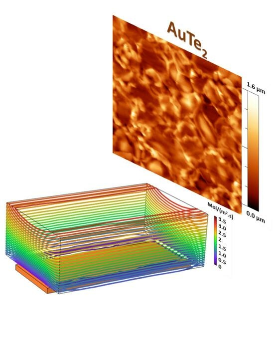
Aiming at studying the silver telluride and gold ditelluride formation based on the tellurization of pre-deposited silver and gold substrates, an AP-CVD system is used. Figure 1a shows the experimental set-up exploited for the growth, consisting of the double-furnace CVD system detailed in the Section 3. Among the key thermodynamic parameters for controlling the tellurization of metallic substrates, we can mention gas flux and temperature during the reaction. Given the kinetic character of the tellurization process, the gas flux is expected to play a significant role in increasing the number of sites for tellurium reaction with the metallic atoms of the substrate. This is supported by finite element method (FEM) simulation used as a guide to optimize the experimental condition (see Section 3 for details). In our experimental setup, typical gas flux values range from 1 sccm to 100 sccm. However, due to the expected low-velocity tellurization reaction in analogy with the sulfurization reaction of metal films [26], we decided to study the condition of the precursor flux magnitude in the range of 1–10 sccm, excluding the highest flux conditions (>10 sccm), which would result in a low residence time of tellurium vapors in the proximity of the metal precursor films. By mapping the FEM contour lines, connecting the points with equal total flux magnitude, we observed a pronounced increment of the contour levels in proximity of the substrate as the gas flux varied from 1 sccm to 100 sccm (see Figure S1a–c in Supplementary Materials). The lower flux magnitude is described by far spacing blue lines in Figure S1a and the higher flux magnitude is represented by more dense red lines in Figure S1b,c. The quantitative comparison of the total flux magnitude across an arbitrary line over the substrate is depicted in Figure S1d. The arbitrary line has a length of 3 cm (equal to the length of the substrate). The y-axis shows the total precursor flux magnitude or, in other terms, the amount of the precursor that is reaching the substrate per unit area per unit time (mol/(m2s)). From the comparison, it is clear that the flux magnitude in the case of 10 sccm carrier gas flow is at least four times higher compared to the 1 sccm flow rate. Although the simulation results reveal a higher precursor flux magnitude over the substrate volume at the carrier gas flux of 100 sccm (Figure S1c), it is not proven to be optimal for the reaction. This is due to the fact that the increase in the carrier gas flux will lead to the reduction in the residence time of the precursor at the vicinity of the substrate. As a conclusion, the FEM simulation clearly indicate that the optimal experimental conditions for the tellurization reaction are obtained at 10 sccm.
According to the literature, the reaction in bulk form between silver and tellurium occurs at 475 °C [24], while the reaction between gold and tellurium is reported at 300–500 °C [27]. In the case of thin films, we studied the growth in the temperature range of 100–350 °C for the downstream furnace under an isobaric condition (pressure of 1 atm/760 torr) and with a 10 sccm Ar/H2 flux (H2 4% vol.) as a carrier gas.
In the first set of experiments, the tellurization of the single-oriented Ag(111)/Mica at 100 °C is studied. The Raman spectra acquired on the tellurized sample is illustrated in Figure 2a and exhibits 7 vibrational modes. According to the literature [17,28], the surface of silver chalcogenides is soft and sensitive to laser power. Consequently, there will be a redox reaction upon the exposure of the laser to the sample surface, which may lead to the decomposition of the silver telluride and the segregation of TeO2 and metallic silver [17,28]. To avoid this issue, we acquired the Raman spectra at the lowest power achievable in our setup (1 mW). The broad spectra acquired on the sample are represented in Figure 2a. The spectra can be decomposed in different spectral components located at 71.0, 91.0, 128.5, 186.3 cm−1, 236.3 cm−1, 349.1 cm−1 and 462.0 cm−1. The peaks located at 91.0 and 128.5 are raised from in-plane E1 and out-of-plane A1 characteristics peaks of Te. The broad peaks at 186.3, 236.3, 349.1 and 462.0 cm−1 are assigned to TeO2 [28,29,30]. The observation of peaks related to the TeO2 may suggest the decomposition of Ag2Te, according to the following reaction: Ag2Te + O2 → 2Ag + TeO2 [17,28]. This leads to the measurement of the Raman peaks of TeO2. Nevertheless, on the local scale, the AFM morphology investigation shows a compact structure of the film. This is confirmed by the topography image acquired on a 2 μm × 2 μm scan area and depicted in Figure 2b, showing the closely packed formation of film with rms roughness value, σ, of 20.1 nm. As demonstrated by the silver and tellurium phase diagram of the reaction [31], the number of possible combinations of the two materials is higher than that of gold and tellurium. Ag2Te occurs in nature as the mineral hessite and can exist in at least three forms. The stoichiometry Ag5Te3 occurs in a mineral called stuetzite, while the metastable phases AgTe, AgTe4 and AgTe2.33 are reported after a very rapid quenching of the molten silver–tellurium alloy [31].
As a result, the control of the reaction product in the CVD system is more complicated in the case of silver tellurization experiments rather than the gold ones. We have investigated the effect of temperature on the growth of silver telluride by changing the temperature from 100 °C to 350 °C while maintaining all the other experimental parameters. According to the literature [28], Raman spectroscopy performed on the sample grown at 350 °C has a different characteristic and shows the formation of a peak at 152 cm−1 (see Figure 2c) that is compatible with the reported spectra of Ag5Te3, which is another compound that exists in the Ag-Te phase diagram. The XPS analysis reported in Figure S2 confirms the chemical coordination between the Ag 3d and Te 3d core levels. This is supported by the fact that the 3d doublet peaks of Te are located at different binding energies (Te 3d5/2~572.2 eV, Te 3d3/2~582.6 eV) compared to the pure elemental state (note that the presence of oxide components is demonstrated by the asymmetry of the spectra). The AFM morphology investigation performed on the 2 μm × 2 μm scan area is represented in Figure 2d and shows the formation of faceted and elongated structures with an RMS roughness of 22.6 nm.
Following the investigation into the tellurization of the Ag substrate on a large scale, the goal is to explore the use of Au as a pre-deposited substrate. The aim is to examine the impact of transitioning from the polycrystalline Au (50 nm)/SiO2 substrate to a single-crystalline Au (111)/Mica and also reducing the thickness of Au/SiO2 from 50 nm down to 10 nm and 5 nm. According to the literature, AuTe2 was synthesized using an aerosol-assisted CVD technique at temperatures around 300–500 °C [27]. It has been shown that samples grown at 300 °C exclusively form monoclinic AuTe2, whereas samples grown at higher temperatures produce Au particles as well, due to the depletion of Te [27]. The tellurization of various Au substrates is carried out under the same experimental conditions as those exploited for the tellurization of the Ag substrate, utilizing the growth temperature of 350 °C (the effect of a slight change of the temperature condition is described in the supporting information file—see Figure S3).
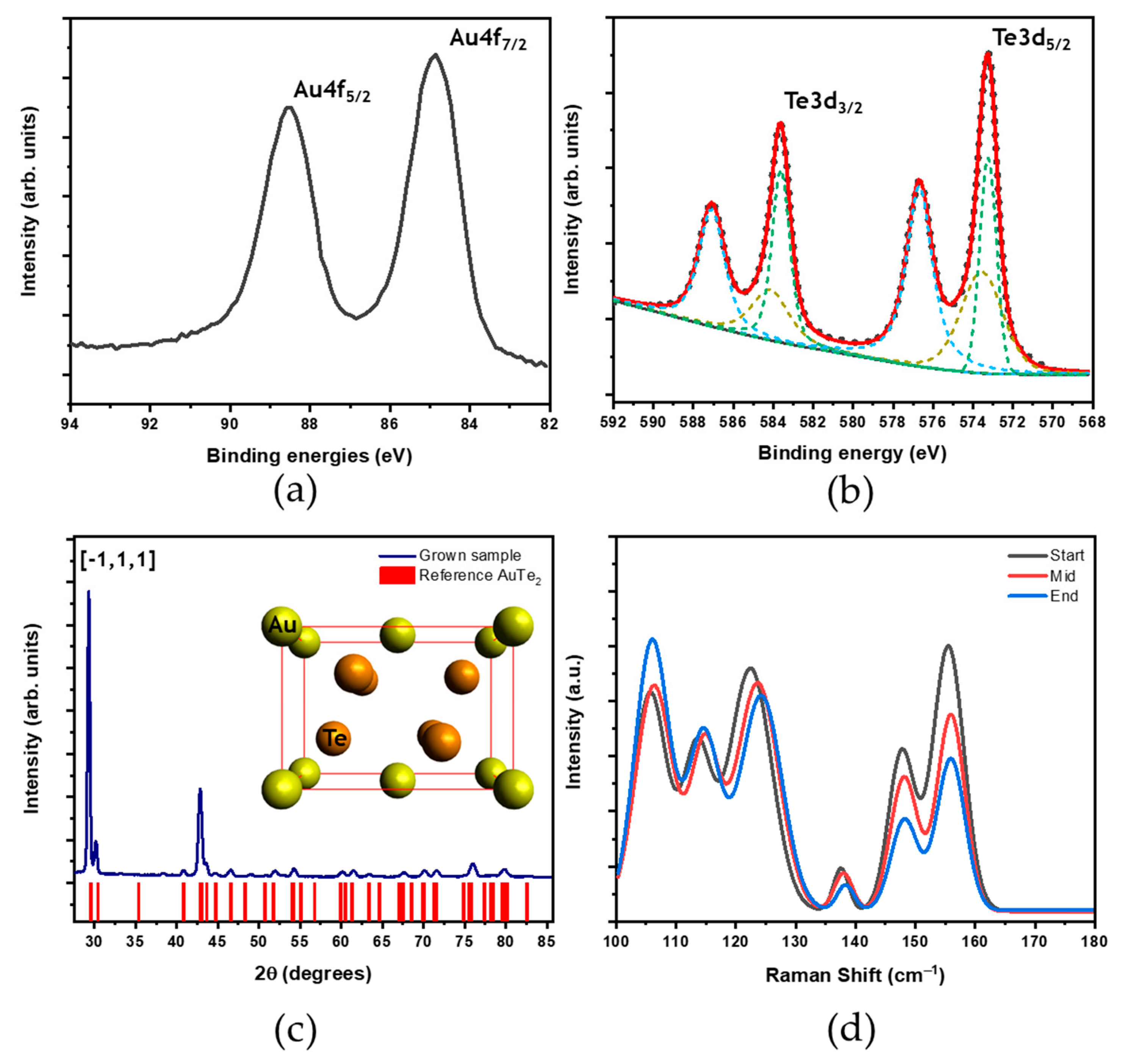
The chemical composition of the grown material is investigated by XPS measurement. The high-resolution Au 4f and Te 3d core levels as a function of binding energy (B.E.) are shown in Figure 3a,b. The experimental data are fitted with a pseudo-Voigt function after background removal. The 4f7/2 and 4f5/2 doublets of Au are located at a higher binding energy (B.E. ~84.8 eV and 88.5 eV, respectively) compared to the pure metallic Au (84 eV and 87.6 eV) [32]; we rationalize this shift of the B.E. with a chemical coordination of the Au atoms with Te atoms in the AuTe2 formation. The Te 3d broad core-level peaks are fitted by two components, where the binding energy of most important peaks, Te 3d5/2 and 3d3/2 (B.E. ~573.2 eV and 583.6 eV, respectively), are related to pure elemental tellurium [11]. The components located at ~576.6 and ~587 eV for 3d5/2 and 3d3/2 can be related to Te oxide due to the exposure to air before the XPS measurement.
To study the crystal structure of the sample, we used XRD analysis. The acquired XRD pattern with the sketch of the crystal structure acquired by Avogadro-1.2.0 software are depicted in Figure 3c. The results show the existence of two main peaks located at nearly 29° and 42.9° relating to the [−1,1,1] and [3,1,0] crystallographic orientation, in addition to few broad peaks matching with the AuTe2 reference pattern [33]. Since AuTe2 exhibits an incommensurately modulated structure, the XRD pattern shows satellites along with main reflections [34]. Therefore, the coordination of gold atoms changes from linear to square planar due to modulation, and the Te zig-zag chains are broken, resulting in isolated Te-Te pairs [32,33]. This average phase has a distorted CdI2 structure,with each Au atom being sixfold coordinated with Te atoms and two long and four short Au-Te bonds. The AuTe6 octahedra form layers parallel to the (001) plane as shown in the inset of Figure 3c [35].
According to the literature [36], the incommensurate modulation of the AuTe2 crystal structure has a strong influence on its optical and vibrational spectrum. In particular, it is responsible for the optical selection rules allowing Raman scattering of phonons with a wavevector q ≠ 0 [36]. As a result, the Raman spectra of the sample after the fitting by the Voigt function and subtraction of the background (due to large background contribution coming from the gold substrate) shows more peaks than expected for a crystal with three atoms per primitive cells [36]. We observed six peaks located at 106.0, 114.1, 123.4, 138.0, 148.0 and 155.7 cm−1 (see Figure 3d). The precise assignment of the peaks to a vibrational mode is not straightforward because of the expected degeneracy of the modes belonging to the different symmetries: Ag, Au and Bg [36]. It is worth to notice that the intensity ratio of the first peaks (located at 106.0 cm−1) with respect to the last peaks (located at 155.7 cm−1) undergoes a variation. In detail, it increases from 0.8 to 1.7, while moving from the region of the sample closer to the tellurium source (named “start point” in plot of Figure 3d) towards the farther region (named “end point” in plot of Figure 3d). On the one hand, we can rationalize this observation by assuming a reduction of the tellurized thickness of the gold film precursor as a function of the position; on the other hand, this demonstrates that the formation of AuTe2 occurs on a large scale (sample area ≈ cm2).
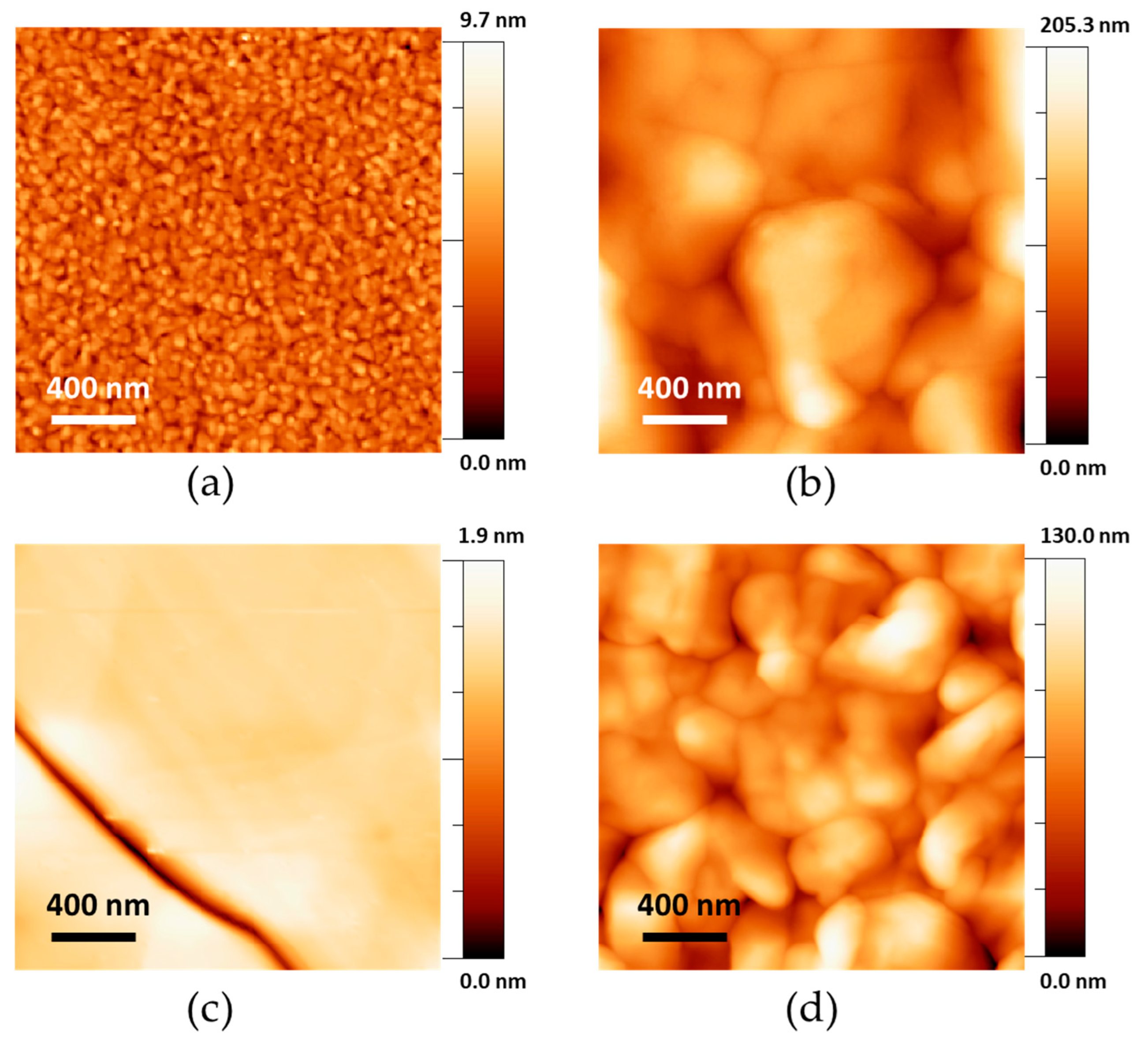
It is interesting to study the morphological features of the grown material at the nanoscale by AFM and make a direct comparison of the morphology of the Au/SiO2 and Au (111)/Mica substrates before and after tellurization (see Figure 4 and Figure S4). As shown in Figure 4a, the surface morphology of the pre-deposited Au on SiO2/Si consists of small grains, whereas the surface morphology of Au (111) film is different and shows a uniform surface (see Figure 4c). The morphology of tellurized Au/SiO2 and Au(111)/Mica films represented in Figure 4b,d, respectively, exhibits the formation of textured material characterized by a continuous and completely covered surface being constituted by large grains. The quantitative estimation of the statistical height distribution is provided by the rms roughness value, σ, in the two cases (see Section 3 The σ variable is derived by analyzing several AFM images (2 µm × 2 µm) acquired at different spatial positions of the sample and by calculating the average value and the statistical standard variation used as uncertainty on the variable. We observe that σ varies from 1.0 ± 0.1 nm in the case of the e-beam deposited Au on SiO2/Si substrate to 33.8 ± 2 nm for the AuTe2 sample after tellurization. Similarly, in the case of Au (111)/Mica, σ varies from 2.7 ± 0.1 nm to 23.1 ± 2 nm for AuTe2 after tellurization. Another statistical parameter derived by our analysis is the mean size of the polycrystalline grains observed in the AFM topographic images. It is worth noting that we applied two different methods for calculating the mean grain size in the topography of Figure 4a with respect to Figure 4b,d (in the case of the Au(111) film. Moreover, the size of the crystalline domains exceeds the typical size of the AFM image, as one can notice in the topography of Figure 4c, where only a small portion of a grain boundaries can be detected in the bottom left part of the map). As noted above, the topography of Figure 4a shows the presence of round-shaped grains obtained by the evaporation of gold atoms on the substrate surface. In this case, we can apply the analysis of the cross-correlation function of the figure to derive the average size of the grains as the full width at half maximum of the correlation peak (see Section 3 and Supplementary Materials for further details). From this analysis, we estimated that for the Au/SiO2 substrate, the average grain size is around 40 ± 2 nm. This method cannot be applied to the topographies of Figure 4b,d due to the fact that the grains show a more irregular shape and spatial distribution. For this reason, we identified the areal distribution of the grains in several AFM images by manually defining the contour line of each single grain and performing statistical calculations on the derived distribution. In the two cases, we observed that after tellurization, the grain size of the AuTe2 reads 870 ± 97 nm (starting from the evaporated gold precursor) and 592 ± 75 nm (starting from the single-crystalline Au(111) film).
The large-scale controlled growth of AuTe2 starting from polycrystalline Au(50 nm)/SiO2 and single-crystalline Au(111)/Mica are successfully demonstrated. The findings reveal that despite the different crystalline characteristics of the substrate (polycrystalline or single-crystalline), the morphological properties of AuTe2 are similar in both cases. The morphological similarity between the tellurized films starting from different substrates (polycrystalline or single-crystalline) demonstrates that the AuTe2 material does not inherit the morphological features of the metallic precursor film. This fact suggests that the mechanism of tellurization does not proceed at the scale of the single gold grain. We speculate that the reaction can occur in two possible ways: The first one is a reaction of the gold and tellurium atoms in the vapor phase and subsequent deposition on the surface. The second one is a reaction between a liquid layer of gold and tellurium vapors at the surface and subsequent re-crystallization. Moreover, after the large-scale synthesizing process of the uniform AuTe2 film, the tellurization of Au/SiO2 substrates with varying thicknesses from 50 nm down to 10 nm and 5 nm will be reported. Figure S5 illustrates the Raman spectra obtained from AuTe2 films with 10 nm and 5 nm pre-deposited Au substrate thicknesses. The Raman peaks identified at 105.6, 115.0, 124.1, 138.5, 148.5 and 156.4 cm−1 (Figure S5) are aligned with the observed Raman spectra of AuTe2 derived from Au with the thickness of 50 nm (in the previous section). The AFM topography images acquired on AuTe2 from Au with the 10 nm and 5 nm thicknesses are represented in Figure 5a,b and show the formation of compact granular grains with average sizes of 142 ± 14 nm and 78 ± 9 nm, respectively (Figure S6). The rms roughness value, σ, exhibits variation between different samples. It ranges from 22.2 ± 1.4 nm for the AuTe2 sample with a 10 nm Au substrate thickness to 10.0 ± 0.6 nm for the AuTe2 sample with a 5 nm Au substrate thickness.
By comparing the calculated average grain size obtained from different Au/SiO2 substrate thicknesses (see Figure 5c), it can be understood that there is a correlation between the initial Au substrate thickness and the resulting grain size of AuTe2 after the tellurization process. It can be interpreted that reducing the thickness of pre-deposited Au on SiO2/Si leads to a smaller grain size. This tellurization method is applicable not only to different gold substrates (polycrystalline and single-crystalline) but also to different thicknesses of gold, ranging from 50 nm to 10 nm and 5 nm.

3. Materials and Methods

3.1. Growth

The ambient pressure CVD (AP-CVD) consists of a double furnace system equipped with a quartz tube reactor of 2″ diameter. Tellurium (Te) powder (40 mg: 99.997%, Sigma Aldrich, Darmstadt, Germany) is exploited as powder precursor. Commercial single-crystal Ag (111) with the thickness of ~300 nm on mica substrate is used. Two different gold substrates are exploited for the experiments: (i) Gold film with 50 nm, 10 nm and 5 nm thicknesses, deposited onto SiO2 (50 nm)/Si substrate by means of e-beam evaporation. (ii) Commercial single-crystal Au(111) with the thickness ~300 nm on mica substrate. The tellurium powder is placed in the middle of ceramic boat in the center of upstream furnace, and the silver and gold substrates with 3 cm × 2 cm dimensions. They are kept on a ceramic boat (face up) parallel to the Te flow direction, and are positioned 18 cm away from the Te powder precursor. The temperatures of 440 °C is set for the upstream furnace (Te powder) and 100 °C or 350 °C is set for the downstream furnace (Ag or Au substrate, respectively), with a 10 sccm Ar/H2 flux (H2 4% volume) as a carrier gas that is flowing for 30 min growth time.

3.2. Characterization

Atomic force microscopy (AFM): The morphology of the samples is investigated in tapping mode by means of commercial AFM (Bruker Dimension Edge) using ultra-sharp silicon tips (TESPA-V2 Bruker radius of curvature 7 nm nominal frequency 320 kHz). Statistical parameters of surface morphology, such as root mean square (RMS) roughness, σ, are derived by means of freely available software (WSxM 4.0, Gwyddion 2.55). The root mean square variation from a height profile is measured by the AFM topographies recurring to the following formula:
σ = 1 N x × N y j = 1 N x i = 1 N y ( h j i < h j i > ) 2
where N x × N y denotes the number of data samples in the topographic matrix along the fast x -scan and low y -scan directions of the AFM acquisition, while h j i is the height acquisition at the j , i position of the matrix. The average height value < h j i > is defined by the following formula:
< h j i > = 1 N x × N y j = 1 N x i = 1 N y h j i
From the AFM images, the self-correlation is defined as follows:
G k 1 ,   k 2 = j = 1 N x i = 1 N y h j i   h j i ( j + k 1 ,   i + k 2 )
This function assesses how different an image is, and the same image is shifted by a distance k 1 and k 2 in the X and Y axis, respectively (starting from the center of the image). The more similar the image and the shifted image are, the higher the value of the self-correlation. For this reason, the highest value is obtained at the center of the image (where k 1 and k 2 are zero). Note that any periodicity in the original image, like the size of the polycrystalline grains, will be shown as a periodic pattern in the self-correlation.
Raman spectroscopy: Vibrational properties of the deposited sample are verified by Raman spectroscopy in z-backscattering geometry using a Renishaw inVia spectrometer equipped with a solid-state laser source of excitation wavelength 514 nm/2.41 eV. The laser source is coupled with an optical microscope and objective with numerical aperture = 0.75 and magnification 50×. The laser power on the sample is kept below 5 mW on the AuTe2 samples and below 1 mW on Ag2Te samples to avoid sample damage.
X-ray diffraction (XRD): XRD patterns were acquired with an HRXRD IS2000 tool equipped with a Cu Kα radiation source, a four-circle goniometer and a curved 120° position-sensitive detector (Inel CPS-120) with angular resolution 0.029°.
X-ray photoelectron spectroscopy (XPS): Chemical composition was probed using an XPS PHI ESCA 5600 with a monochromatic Al X-ray source and a hemispherical analyzer with pass energy 5.85 eV, energy step 0.025 eV and energy resolution 0.1 eV.

3.3. Finite Element Method (FEM) Simulations

The three-dimensional simulation of fluid flow dynamics coupled with mass and heat transfer in a CVD growth reactor was solved by finite element method (FEM) in COMSOL Multiphysics environment. This model involves using Navier–Stokes equation, mass diffusion, conduction and convection heat transfer solved within FEM scheme, taking into account different initial and boundary conditions [37]. The solution obtained from the simulation predicts the carrier gas velocity, concentration of precursor and temperature distribution within the furnace providing insights about macroscale growth parameters. In detail, the Navier–Stokes equation governing the laminar flow is as follows:
ρ u t + u · u = p + · μ u + u T 2 3 μ · u I + F ; ρ t + · ρ u = 0
where u is the velocity field, ρ is the mass density, μ the dynamic viscosity, p the pressure, I the unit matrix and F the volumetric applied force (i.e., gravity). The superscript T represents the transposed matrix.
The equation describing the mass transport is as follows:
R = c t + · D c + u · c ; N = D c + u
where R is the source term for precursor, c is the precursor concentration, D is the diffusion coefficient and N is the flux of the precursor.
The conduction and convection heat transfer are described by the following equation:
Q = ρ C p T t + ρ C p u · T + · q ; q = k T
where Q is the heat source, Cp is the specific heat of gas, k is thermal conductivity and T is temperature.

4. Conclusions

This study introduces a scalable CVD method for the growth of Ag2Te and AuTe2 ultrathin films by tellurizing the pre-deposited Ag and Au substrates on a cm2 scale area. Regarding the tellurization of Ag films at the optimal experimental conditions (temperature of 350 °C and atmospheric pressure), the results suggest the formation of Ag and Te compounds mainly in the Ag5Te3 stoichiometry. Moreover, for the Au substrates, we showed that the tellurization method is effective for obtaining ultrathin AuTe2 films. The growth of AuTe2 is triggered by maintaining the temperature at 350 °C, which is optimal for the tellurization reaction on the Au substrate. By employing the tellurization growth method, resulting AuTe2 films grown on Au substrates can be harnessed for the applications in thermoelectric, nanoelectronic and optoelectronic devices. Furthermore, this growth method is adaptable for the tellurization of single-crystalline Au (111)/Mica and thinner Au films with thicknesses as low as 5 nm.

Supplementary Materials

The following supporting information can be downloaded at: https://0-www-mdpi-com.brum.beds.ac.uk/article/10.3390/inorganics12010033/s1. Figure S1: FEM simulation results of the precursor (tellurium powder) flux (represented by colorful contour lines) at the volume (cube) above the substrate (depicted in orange color) for different carrier gas fluxes. Figure S2: X-ray photoelectron spectroscopy (XPS) of silver telluride. Figure S3: Effect of temperature on the growth of AuTe2. Figure S4: Large-scale AFM topographies of the AuTe2 obtained, starting from the evaporated Au on SiO2/Si and single-crystal Au/Mica. Figure S5: Raman spectra acquired on AuTe2 films starting from Au films with thicknesses 10 nm and 5 nm, respectively. Figure S6: Self-correlation function of the AFM topography.

Author Contributions

Conceptualization, C.M., A.L., C.G. and A.M.; methodology, S.G., C.M., A.L., M.A., C.G. and A.M.; formal analysis, S.G.; investigation, S.G.; writing—original draft preparation, S.G. and C.M.; writing—review and editing, S.G., C.M., A.L., M.A., C.G., C.S.C. and A.M.; supervision, C.M., C.S.C. and A.M.; funding acquisition, A.M. All authors have read and agreed to the published version of the manuscript.

Funding

This work was financially supported by the European Commission under the H2020 ERC-COG grant nr. 772261 “XFab” and Ministero Università e Ricerca (MUR) under the PRIN project “PHOTO” nr. 2020RPEPNH.

Data Availability Statement

The data presented in this study are available in this article and the Supplementary Materials.

Acknowledgments

We acknowledge Simone Cocco (CNR-IMM) for his technical support. We acknowledge Eleonora Bonaventura (University of Milano Bicocca) for her assistance in Raman spectroscopy acquisition.

Conflicts of Interest

The authors declare no conflicts of interest.

References

  1. Shi, Y.; Sturm, C.; Kleinke, H. Chalcogenides as Thermoelectric Materials. J. Solid State Chem. 2019, 270, 273–279. [Google Scholar] [CrossRef]
  2. Jamwal, D.; Mehta, S.K. Metal Telluride Nanomaterials: Facile Synthesis, Properties and Applications for Third Generation Devices. ChemistrySelect 2019, 4, 1943–1963. [Google Scholar] [CrossRef]
  3. Martella, C.; Quadrelli, A.; Tummala, P.P.; Lenardi, C.; Mantovan, R.; Lamperti, A.; Molle, A. Tailoring the Phase in Nanoscale MoTe2 Grown by Barrier-Assisted Chemical Vapor Deposition. Cryst. Growth Des. 2021, 21, 2970–2976. [Google Scholar] [CrossRef]
  4. Tummala, P.P.; Ghomi, S.; Casari, C.S.; Martella, C.; Lamperti, A.; Molle, A. Large Area Growth and Phase Selectivity of MoTe2 Nanosheets through Simulation-Guided CVD Tellurization. Adv. Mater. Interfaces 2023, 10, 2200971. [Google Scholar] [CrossRef]
  5. Li, J.; Cheng, S.; Liu, Z.; Zhang, W.; Chang, H. Centimeter-Scale, Large-Area, Few-Layer 1T′-WTe2 Films by Chemical Vapor Deposition and Its Long-Term Stability in Ambient Condition. J. Phys. Chem. C 2018, 122, 7005–7012. [Google Scholar] [CrossRef]
  6. Charoenphakdee, A.; Kurosaki, K.; Harnwunggmoung, A.; Muta, H.; Yamanaka, S. Thermoelectric Properties of Gold Telluride: AuTe2. J. Alloys Compd. 2010, 496, 53–55. [Google Scholar] [CrossRef]
  7. Kim, S.; Ryu, S.H.; Kwon, Y.-T.; Lim, H.-R.; Park, K.-R.; Song, Y.; Choa, Y.-H. Synthesis and Thermoelectric Characterization of High Density Ag2Te Nanowire/PMMA Nanocomposites. Mater. Chem. Phys. 2017, 190, 187–193. [Google Scholar] [CrossRef]
  8. Xu, Y.; Yan, M.; Jiang, E.; Zheng, Z.; Wang, H.; Duan, B.; Li, G.; Zhai, P. Thermoelectric Properties of Ag2Te Prepared by One-Step Hot-Pressing Method. Mater. Lett. 2023, 339, 134100. [Google Scholar] [CrossRef]
  9. Fujikane, M.; Kurosaki, K.; Muta, H.; Yamanaka, S. Thermoelectric Properties of α- and β-Ag2Te. J. Alloys Compd. 2005, 393, 299–301. [Google Scholar] [CrossRef]
  10. Kitagawa, S.; Kotegawa, H.; Tou, H.; Ishii, H.; Kudo, K.; Nohara, M.; Harima, H. Pressure-Induced Superconductivity in Mineral Calaverite AuTe2. J. Phys. Soc. Jpn. 2013, 82, 113704. [Google Scholar] [CrossRef]
  11. Kudo, K.; Ishii, H.; Takasuga, M.; Iba, K.; Nakano, S.; Kim, J.; Fujiwara, A.; Nohara, M. Superconductivity Induced by Breaking Te2 Dimers of AuTe2. J. Phys. Soc. Jpn. 2013, 82, 063704. [Google Scholar] [CrossRef]
  12. Zhang, Y.; Li, Y.; Ma, Y.; Li, Y.; Li, G.; Shao, X.; Wang, H.; Cui, T.; Wang, X.; Zhu, P. Electronic Topological Transition in Ag2Te at High-Pressure. Sci. Rep. 2015, 5, 14681. [Google Scholar] [CrossRef]
  13. Guo, L.; Tan, L.; Xu, A.; Li, G.; Zhang, G.; Liu, R.; Wang, J.; Du, Y.; Dang, F. Highly Efficient Two-Dimensional Ag2Te Cathode Catalyst Featuring a Layer Structure Derived Catalytic Anisotropy in Lithium-Oxygen Batteries. Energy Storage Mater. 2022, 50, 96–104. [Google Scholar] [CrossRef]
  14. Zhu, J.; Pandey, R. Silver Tellurides: Structural, Elastic, and Optical Properties of AgTe and Ag2Te. J. Phys. Chem. Solids 2019, 129, 41–45. [Google Scholar] [CrossRef]
  15. Wang, W.; Liu, J.; Li, X.; Jiang, Q.; Xu, J.; Luo, C.; Liu, P.; Tan, R.; Du, Y.; Jiang, F. Galvanic Exchange Reaction Involving Te Nanowires and Ag Ions for N-Type Te/Ag2Te Thermoelectric Nanofilms. J. Nanopart. Res. 2019, 21, 131. [Google Scholar] [CrossRef]
  16. Chang, Y.; Guo, J.; Tang, Y.-Q.; Zhang, Y.-X.; Feng, J.; Ge, Z.-H. Facile Synthesis of Ag2Te Nanowires and Thermoelectric Properties of Ag2Te Polycrystals Sintered by Spark Plasma Sintering. CrystEngComm 2019, 21, 1718–1727. [Google Scholar] [CrossRef]
  17. Qin, A.; Fang, Y.; Tao, P.; Zhang, J.; Su, C. Silver Telluride Nanotubes Prepared by the Hydrothermal Method. Inorg. Chem. 2007, 46, 7403–7409. [Google Scholar] [CrossRef]
  18. Zhong, B.; Wang, X.; Bi, Y.; Kang, W.; Zhang, L. Simple Synthesis of Crooked Ag2Te Nanotubes and Their Photoelectrical Properties. New J. Chem. 2021, 45, 6100–6107. [Google Scholar] [CrossRef]
  19. Park, D.; Ju, H.; Kim, J. Enhanced Thermoelectric Power Factor and Low Thermal Conductivity in One-Dimensional Te/Ag2Te Composites. Ceram. Int. 2017, 43, 11156–11162. [Google Scholar] [CrossRef]
  20. Hansen, M.; Anderko, K.; Salzberg, H.W. Constitution of Binary Alloys. J. Electrochem. Soc. 1958, 105, 2600. [Google Scholar] [CrossRef]
  21. Streltsov, S.V.; Roizen, V.V.; Ushakov, A.V.; Oganov, A.R.; Khomskii, D.I. Old Puzzle of Incommensurate Crystal Structure of Calaverite AuTe2 and Predicted Stability of Novel AuTe Compound. Proc. Natl. Acad. Sci. USA 2018, 115, 9945–9950. [Google Scholar] [CrossRef]
  22. Ootsuki, D.; Takubo, K.; Kudo, K.; Ishii, H.; Nohara, M.; Saini, N.L.; Sutarto, R.; He, F.; Regier, T.Z.; Zonno, M.; et al. Effect of Pt Substitution on the Electronic Structure of AuTe2. Phys. Rev. B 2014, 90, 144515. [Google Scholar] [CrossRef]
  23. Palyanova, G.A.; Tolstykh, N.D.; Zinina, V.Y.; Kokh, K.A.; Seryotkin, Y.V.; Bortnikov, N.S. Synthetic Gold Chalcogenides in the Au–Te–Se–S System and Their Natural Analogs. Dokl. Earth Sci. 2019, 487, 929–934. [Google Scholar] [CrossRef]
  24. Grasser, M.A.; Pietsch, T.; Brunner, E.; Doert, T.; Ruck, M. Low Temperature Activation of Tellurium and Resource-Efficient Synthesis of AuTe2 and Ag2Te in Ionic Liquids. ChemistryOpen 2021, 10, 117–124. [Google Scholar] [CrossRef]
  25. Bouaziz, M.; Zhang, W.; Tong, Y.; Oughaddou, H.; Enriquez, H.; Mlika, R.; Korri-Youssoufi, H.; Chen, Z.; Xiong, H.; Cheng, Y.; et al. Phase Transition from Au–Te Surface Alloy towards Tellurene-like Monolayer. 2D Mater. 2020, 8, 015029. [Google Scholar] [CrossRef]
  26. Vangelista, S.; Cinquanta, E.; Martella, C.; Alia, M.; Longo, M.; Lamperti, A.; Mantovan, R.; Basset, F.B.; Pezzoli, F.; Molle, A. Towards a Uniform and Large-Scale Deposition of MoS2 Nanosheets via Sulfurization of Ultra-Thin Mo-Based Solid Films. Nanotechnology 2016, 27, 175703. [Google Scholar] [CrossRef] [PubMed]
  27. Copsey, M.C.; Panneerselvam, A.; Afzaal, M.; Chivers, T.; O’Brien, P. Syntheses, X-ray Structures and AACVD Studies of Group 11 Ditelluroimidodiphosphinate Complexes. Dalton Trans. 2007, 15, 1528–1538. [Google Scholar] [CrossRef]
  28. Milenov, T.I.; Tenev, T.; Miloushev, I.; Avdeev, G.V.; Luo, C.W.; Chou, W.C. Preliminary Studies of the Raman Spectra of Ag2Te and Ag5Te3. Opt. Quantum Electron. 2014, 46, 573–580. [Google Scholar] [CrossRef]
  29. Vasileiadis, T.; Yannopoulos, S.N. Photo-Induced Oxidation and Amorphization of Trigonal Tellurium: A Means to Engineer Hybrid Nanostructures and Explore Glass Structure under Spatial Confinement. J. Appl. Phys. 2014, 116, 103510. [Google Scholar] [CrossRef]
  30. Champarnaud-Mesjard, J.C.; Blanchandin, S.; Thomas, P.; Mirgorodsky, A.; Merle-Méjean, T.; Frit, B. Crystal Structure, Raman Spectrum and Lattice Dynamics of a New Metastable Form of Tellurium Dioxide: γ-TeO2. J. Phys. Chem. Solids 2000, 61, 1499–1507. [Google Scholar] [CrossRef]
  31. Karakaya, I.; Thompson, W.T. The Ag-Te (Silver-Tellurium) System. JPE 1991, 12, 56–63. [Google Scholar] [CrossRef]
  32. Van Triest, A.; Folkerts, W.; Haas, C. Electronic Structure and Photoelectron Spectra of Calaverite, AuTe2. J. Phys. Condens. Matter 1990, 2, 8733. [Google Scholar] [CrossRef]
  33. Schutte, W.J.; de Boer, J.L. Valence Fluctuations in the Incommensurately Modulated Structure of Calaverite AuTe2. Acta Crystallogr. Sect. B 1988, 44, 486–494. [Google Scholar] [CrossRef]
  34. Wang, Z.; Wang, L.; Huang, J.; Wang, H.; Pan, L.; Wei, X. Formation of Single-Crystal Tellurium Nanowires and Nanotubes via Hydrothermal Recrystallization and Their Gas Sensing Properties at Room Temperature. J. Mater. Chem. 2010, 20, 2457–2463. [Google Scholar] [CrossRef]
  35. Caracas, R.; Gonze, X. Structural, Electronic, and Dynamical Properties of Calaverite AuTe2 under Pressure. Phys. Rev. B 2004, 69, 144114. [Google Scholar] [CrossRef]
  36. Van Loosdrecht, P.H.M.; van Bentum, P.J.M.; Balzuweit, K. Raman Study of Incommensurately Modulated Calaverite (AuTe2). Ferroelectrics 1992, 125, 517–522. [Google Scholar] [CrossRef]
  37. Ghomi, S.; Tummala, P.P.; Cecchini, R.; Casari, C.S.; Lamperti, A.; Grazianetti, C.; Martella, C.; Molle, A. Tailoring the Dimensionality of Tellurium Nanostructures via Vapor Transport Growth. Mater. Sci. Semicond. Process. 2023, 168, 107838. [Google Scholar] [CrossRef]
Figure 1. (a) Schematic view of the experimental setup for the CVD grown silver telluride and gold telluride. (b) Temperature ramp applied to the upstream is 440 °C and 100 °C (or 350 °C) to the downstream for the growth of the silver telluride and 350 °C for the gold telluride.
Inorganics 12 00033 g001
Figure 2. (a) Raman spectra acquired on the Ag2Te sample grown at 100 °C and excited at 514 nm with 3 mW laser power (orange curve: fitted curve; colored curves: fitting components). (b) AFM topography image performed on 2 μm × 2 μm scan area of Ag2Te sample grown at 100 °C. (c) Raman spectra acquired on the Ag5Te3 sample grown at 350 °C and excited at 514 nm with 3 mW laser power. (d) AFM topography image performed on 2 μm × 2 μm scan area of Ag5Te3 sample grown at 350 °C.
Inorganics 12 00033 g002
Figure 3. (a) Au 4f and (b) Te 3d spectral regions from XPS (red curve: fitted curve, color dashed lines: fitting components, dashed black curve: raw data). (c) XRD pattern taken from the AuTe2 sample and the peak position of the reference; inset crystal structure of AuTe2 imported from Avogadro-1.2.0 software. (d) Raman spectra acquired on the AuTe2 excited at 514 nm and the Raman measurement performed at start, middle and end points of the sample.
Inorganics 12 00033 g003
Figure 4. AFM topography image acquired on 2 μm × 2 μm scan area of (a) Au/SiO2 substrate before tellurization. (b) AuTe2 starting from Au/SiO2 after tellurization. (c) Au(111)/Mica substrate before tellurization. (d) AuTe2 starting from Au(111)/Mica after tellurization.
Inorganics 12 00033 g004
Figure 5. (a) AFM topography image acquired on 2 μm × 2 μm scan area performed on AuTe2 with 10 nm Au thickness and (b) 5 nm Au thickness (c) comparison of the average grain size and rms roughness of AuTe2 grown from 50 nm, 10 nm, and 5 nm Au substrates.
Inorganics 12 00033 g005
Disclaimer/Publisher’s Note: The statements, opinions and data contained in all publications are solely those of the individual author(s) and contributor(s) and not of MDPI and/or the editor(s). MDPI and/or the editor(s) disclaim responsibility for any injury to people or property resulting from any ideas, methods, instructions or products referred to in the content.

