
Introductory Overview of Layer Formation Techniques of Ag Nanowires on Flexible Polymeric Substrates

1
Department of Intelligent Semiconductor Engineering, Chung-Ang University, Seoul 06974, Republic of Korea
2
Material Science and Engineering, Physical Science and Engineering Division, King Abdullah University of Science and Technology (KAUST), Thuwal 04700, Saudi Arabia
3
School of Integrative Engineering, Chung-Ang University, Seoul 06974, Republic of Korea
*
Author to whom correspondence should be addressed.
Inorganics 2024, 12(3), 65; https://0-doi-org.brum.beds.ac.uk/10.3390/inorganics12030065
Submission received: 30 November 2023
/
Revised: 18 February 2024
/
Accepted: 21 February 2024
/
Published: 21 February 2024
(This article belongs to the Special Issue Optical and Quantum Electronics: Physics and Materials)
Abstract
:Ag nanowire electrodes are promising substitutes for traditional indium tin oxide (ITO) electrodes in optoelectronic applications owing to their impressive conductivity, flexibility, and transparency. This review provides an overview of recent trends in Ag nanowire electrode layer formation, including key developments, challenges, and future prospects. It addresses several challenges in integrating Ag nanowires into practical applications, such as scalability, cost-effectiveness, substrate compatibility, and environmental considerations. Additionally, drawing from current trends and emerging technologies, this review explores potential avenues for improving Ag nanowire layer-forming technologies, such as material advancements, manufacturing scalability, and adaptability to evolving electronic device architectures. This review serves as a resource for researchers, engineers, and stakeholders in nanotechnology and optoelectronics, and underscores the relationship between advancements in patterning and the application of Ag nanowire electrodes. Through an examination of key developments, challenges, and future prospects, this review contributes to the collective knowledge base and encourages continued innovation in the ever-evolving realm of Ag nanowire-based optoelectronics.
1. Introduction
In the evolving fields of electronic engineering and optoelectronics, scientists and engineers are constantly searching for materials that can outperform indium tin oxide (ITO). The scarcity and cost fluctuations of indium, along with environmental concerns related to its extraction, challenge its long-term viability. Additionally, the adaptability of ITO to emerging technologies is limited by its brittleness, which reduces its durability, especially on flexible substrates, and its low conductivity at lower thicknesses [1,2,3,4,5,6,7,8]. As a result, there is increasing demand for electronic components that offer not only high performance but also environmental sustainability. In this context, Ag nanowires have emerged as a promising alternative owing to their excellent electrical conductivity, inherent flexibility, and outstanding transparency [9,10,11,12,13,14,15,16,17], which makes them a leading choice for next-generation electronics such as flexible displays and wearable devices [18,19,20,21,22,23,24,25]. Consequently, extensive research has been conducted on the synthesis, characterization, and applications of Ag nanowires (Figure 1) [26].
Layer formation technologies play a crucial role in unlocking the full potential of Ag nanowire electrodes, especially in the context of how form and function interact. By overcoming the technical challenges associated with Ag nanowire layer formation, the theoretical benefits of Ag nanowires can be translated into practical applications [5,12,27,28,29,30,31,32]. This review examines recent developments in the formation of Ag nanowire electrode layers [9,10,13,20,33,34,35] and highlights the associated challenges and opportunities, including scalability, cost-efficiency, material compatibility, and environmental considerations. The primary aim is to provide an overview of the multifaceted challenges faced by researchers and industry in utilizing Ag nanowires in actual devices. Furthermore, this review explores the future potential of Ag nanowire layers and their integration into evolving electronic designs and the opportunities they offer for improving the electrode potential of optoelectronic devices. It aims to provide accessible knowledge beneficial to researchers, engineers, industry professionals, and policymakers.
2. Methods for Ag nanowire Layer Formation
The development of transparent conductive films on flexible polymeric substrates has led to significant advancements in coating techniques to improve the performance and applicability of the resulting films. Ag nanowires are increasingly recognized as candidates for transparent conductive layers in diverse applications, such as flexible electronics and solar cells, owing to their excellent electrical conductivity and optical transparency. Choosing an appropriate coating method is crucial, as it greatly affects the characteristics of the film and its suitability for a given application. The following sections explore different coating methods, including their operating principles, recent advancements and challenges, and the interaction between the coating method and the characteristics of the base material.
2.1. Spray Coating
Spray coating is a versatile and cost-effective method for depositing Ag nanowires on both rigid and flexible substrates [14,36,37,38]. This technique is simple and able to cover large areas uniformly. Recent advancements in spray coating have focused on refining precision, particularly with regard to nanowire density and orientation. Researchers are exploring novel approaches to optimize the spray parameters, such as the solvent composition and nozzle design, to enhance the homogeneity of the resultant films. In a notable example of these achievements, Zhu et al. developed a solvent-welding technique employing Ag nanowire spray coating (Figure 2) [36]. Ag nanowire networks combined with poly(vinylpyrrolidone) (PVP) and camphorquinone were spray coated onto a substrate containing ethylene glycol. By applying a current to the Ag nanowire network, the electrical resistance was reduced by a significant 96%. The versatility of spray-coating in terms of material selection and scalability makes it a valuable solution for wide-ranging applications, from small-scale laboratory research to large-scale industrial manufacturing. The ability to generate uniform and transparent conductive films through spray coating is particularly promising for the advancement of technologies such as flexible displays, touchscreens, and solar cells [14,36,37,38]. Furthermore, this method is cost-effective for the production of transparent conductive films. Advances in the spray-coating of Ag nanowire films on flexible polymeric substrates will facilitate the fabrication of next-generation transparent conductive films for diverse applications.
2.2. Dip Coating
Dip coating involves submerging a substrate in an Ag nanowire solution [37,39,40,41,42]. This method offers excellent control over the film thickness; however, achieving uniformity over large areas remains challenging. Therefore, recent research on dip-coating is focused on overcoming this limitation. In a recent study, Zeng et al. used dip coating to fabricate Ag nanowire electrodes on polyethylene terephthalate (PET) fabrics (Figure 3) [43], followed by hot pressing to improve the adhesion of the Ag nanowires to the fabric. This approach resulted in fabric with excellent electrical conductivity (of 464.2 S/m); strong electromagnetic shielding (17 dB); good strain sensing performance; minimal resistance changes (below −15%); and outstanding Joule-heating performance (110 °C at a current of 0.08 A). In the work by Choi et al., aligned Ag nanowire electrodes were fabricated with the dip-coating process [42]. They fabricated differently aligned Ag nanowire electrodes for flexible strain sensors, which were aligned longitudinally, parallel to the alignment direction, and the other aligned laterally, perpendicular to it (Figure 4). The sensor performance results indicated that the strain sensor with the longitudinally aligned Ag nanowire electrodes exhibited a gauge factor (GF) of 89.99 under 25% tensile strain, surpassing the GF of 12.71 of that with laterally aligned Ag nanowire electrodes. Other innovations such as advanced withdrawal techniques and modifications to the solution rheology have also been explored to enhance the uniformity of dip-coated films. Despite the challenges in achieving large-scale uniformity, dip coating remains a valuable tool, especially for applications and electronic components that require precise thickness control [37,39,40,41,42].
2.3. Roll-to-Roll Coating
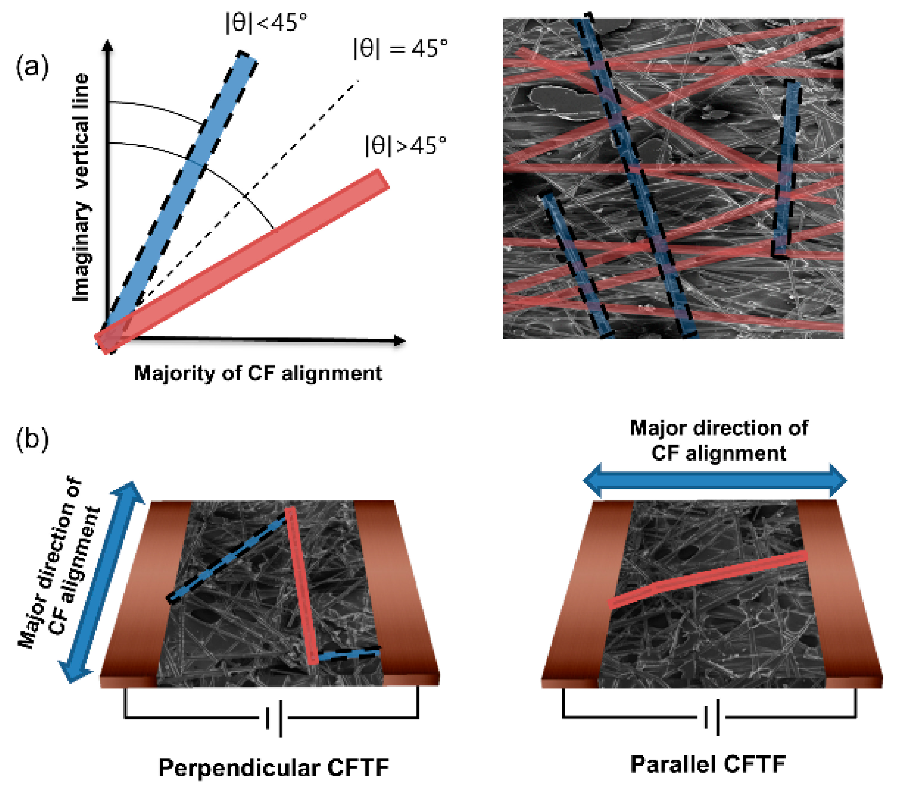
Roll-to-roll (R2R) coating is a popular method of producing transparent conductive films, particularly in large-scale manufacturing [39,44,45,46,47]. This method involves continuously applying an Ag nanowire solution to a flexible substrate as it moves between rolls. The continuous nature of R2R coating makes it highly efficient for mass production. Consequently, it is particularly promising for products that require high-volume outputs, including flexible electronics and large-area photovoltaic cells. Furthermore, it is compatible with existing manufacturing processes, which offers significant advantages. Recently, Jeong et al. created a transparent conductive film made of an Ag nanowire-PVP composite through R2R coating (Figure 5) [48]. They achieved selective calendering by continuous R2R patterning using an embossed pattern roll, resulting in a pattern line width of 0.1 mm and spacing of 1 mm. R2R coating also has the ability to align the Ag nanowires by adjusting the coating conditions (Figure 6) [49]. Current research on R2R coating is focused on further innovations such as optimizing the drying process and improving the substrate-handling systems, which will enhance its efficiency and applicability to diverse industrial applications [39,44,45,46,47].
2.4. Spin Coating
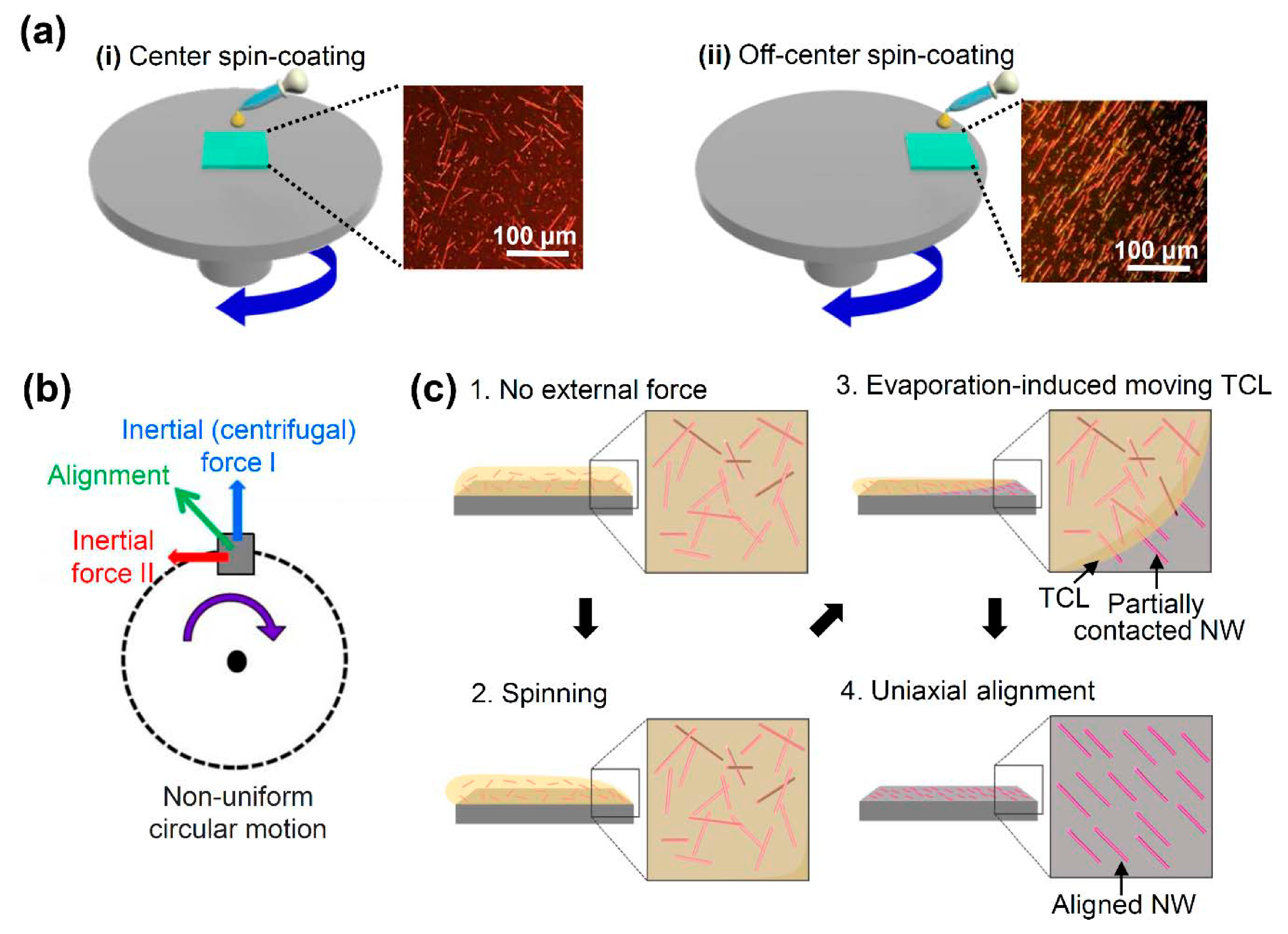
Spin coating is a prevalent method of applying thin films to substrates at laboratory scale [50,51,52,53]. This method involves spinning a substrate to evenly distribute an Ag nanowire solution over it, which offers precise control over the film thickness. However, its scalability is somewhat limited compared to other coating techniques. Current research on spin coating is focused on expanding its applicability by investigating new spinning techniques, exploring alternative solvents, and optimizing spin parameters to achieve larger-scale uniformity without compromising precision. For example, Zhang et al. prepared an Ag nanowire electrode by spin coating (Figure 7) [54]. They compared four common experimental methods, that is, Mayer rod coating, spin coating, spray coating, and vacuum filtration, to create transparent conductive films using a single type of Ag nanowire. Among the coating methods, spin coating was found to be well-suited for preparing small-sized Ag nanowire films that displayed excellent bending stability. By contrast, spray coating required precise control of the process parameters such as spray distance and traveling speed to obtain uniform Ag nanowire coatings; vacuum filtration required longer times to form Ag nanowire layers; and Mayer rod coating posed the risk of scratching the substrate owing to direct rod contact. Therefore, spin coating remains a valuable technique in research and development, especially for producing uniform films for in-depth electrical, optical, and mechanical analyses [50,51,52,53]. In addition, Lee et al. found that the spin coating can produce differently aligned Ag nanowire electrodes by adjusting the spin coating conditions (Figure 8) [55].
2.5. Doctor-Blade Coating
Doctor-blade coating is a precise technique for spreading Ag nanowire solutions onto substrates using a specialized blade [56,57,58]. This method offers meticulous control over the film thickness and uniformity, making it particularly promising for applications where these characteristics are paramount. Recent developments in doctor-blade coating have focused on improving the blade design and exploring innovative materials for the blade itself to refine the coating process. Yoon et al. studied the effect of doctor-blading conditions on the electrical properties of Ag nanowire electrodes (Figure 9) [59]. The blade height and speed were the main parameters that determined the electrical properties of the Ag nanowire electrodes. They found that a lower blade height correlated with lower electrical resistance, and that the optimal blade speed was 20 mm/s. The ability to tailor the film properties using this technique makes it a valuable tool in both research and industrial settings. Consequently, doctor-blade coating is likely to see increasing use to meet the growing demand for tailored transparent conductive films [56,57,58].
Doctor-blade coating shows excellent promise for the large-scale and cost-effective production of transparent conductive films on flexible polymeric substrates for applications including flexible electronics, touchscreens, and solar cells. This underscores the versatility and practicality of doctor-blade coating. Current research in this area is focused on exploring alternative materials, sustainable fabrication techniques, and integration with emerging technologies, highlighting the potential for continued innovation in doctor-blade-coated transparent conductive films.
2.6. Inkjet Printing
Inkjet printing is a digital deposition method that has gained popularity for its ability to precisely deposit Ag nanowire ink in controlled patterns on diverse substrates [60,61,62,63]. This technique enables intricate designs and patterns to be created, making it ideal for producing electronic circuits and displays. Recent innovations in inkjet printing technologies have focused on enhancing the printing resolution, exploring new ink formulations, and expanding substrate compatibility. For example, Wu et al. prepared Ag nanowire flexible transparent conductive films by inkjet printing (Figure 10) [64]. They tailored various factors, such as the surface tension and viscosity of the ink and the contact angle between the Ag nanowire ink droplet and PET substrate, and investigated the effect on the electrical properties of the prepared Ag nanowire layer. The best optical and electrical properties were achieved when using an Ag nanowire ink with a concentration of 0.38–0.57 mg/mL and a post-coating heat treatment at 60 °C for 10 min. In addition, Reenaers et al. showed that the final performance of electrodes fabricated by ink jet printing was mainly influenced by the post-sintering conditions (Figure 11) [65]. The adaptability of inkjet printing to different substrates, including flexible ones, makes it a promising method for applications requiring intricate designs and patterns, including advanced electronic devices and wearable technologies [60,61,62,63].
2.7. Electrospinning
Electrospinning is a less conventional yet innovative approach for preparing Ag nanowire films. This technique involves generating a nanofiber web on a substrate that captures Ag nanowires [66,67,68,69,70]. This method is particularly relevant for specialized applications that require the formation of nanofiber networks. Recent research in this area has focused on enhancing the nanofiber control, optimizing the solution parameters, and expanding the range of compatible substrates. Wang et al. deposited Ag nanowires on a stretchable thermoplastic polyurethane (TPU) substrate to fabricate a stretchable pressure sensor (Figure 12) [66]. The electrospun Ag nanowire layer exhibited high directionality, which was advantageous for directional sensing. The Ag nanowire/TPU electrode pressure sensor demonstrated excellent sensing performance, with a sensitivity of 7.24 kPa−1 within the range of 9.0 × 10⁻³ to 0.98 kPa. Notably, the versatility and potential of electrospinning for applications beyond traditional transparent conductive film applications, such as sensors and advanced filtration systems, demonstrates the impact of further research in this field [66,67,68,69,70].
2.8. Gravure Printing
Gravure printing, also known as rotogravure printing, is a high-throughput technique for transferring ink from engraved cells or depressions on a printing cylinder to a substrate [71,72,73,74]. The engraved cells are filled with ink, after which excess ink is removed from the surface, leaving ink only in the depressions. The substrate is then rolled over the cylinder to transfer the patterned ink. This technique is particularly beneficial in the field of printed electronics, as it offers an efficient and cost-effective method of producing conductive patterns, including electrodes, on various substrates. When applied to the deposition of Ag nanowires, gravure printing combines the advantages of traditional intaglio printing with the unique properties of Ag nanowires, resulting in the preparation of flexible and transparent conductive films suitable for diverse applications [75]. Notably, gravure printing allows precise control over the amount of ink transferred, ensuring uniformity of the electrode pattern. This is particularly important for applications such as electronic devices, because the performance is highly dependent on the consistency and reproducibility of the deposited film [71,72,73,74].
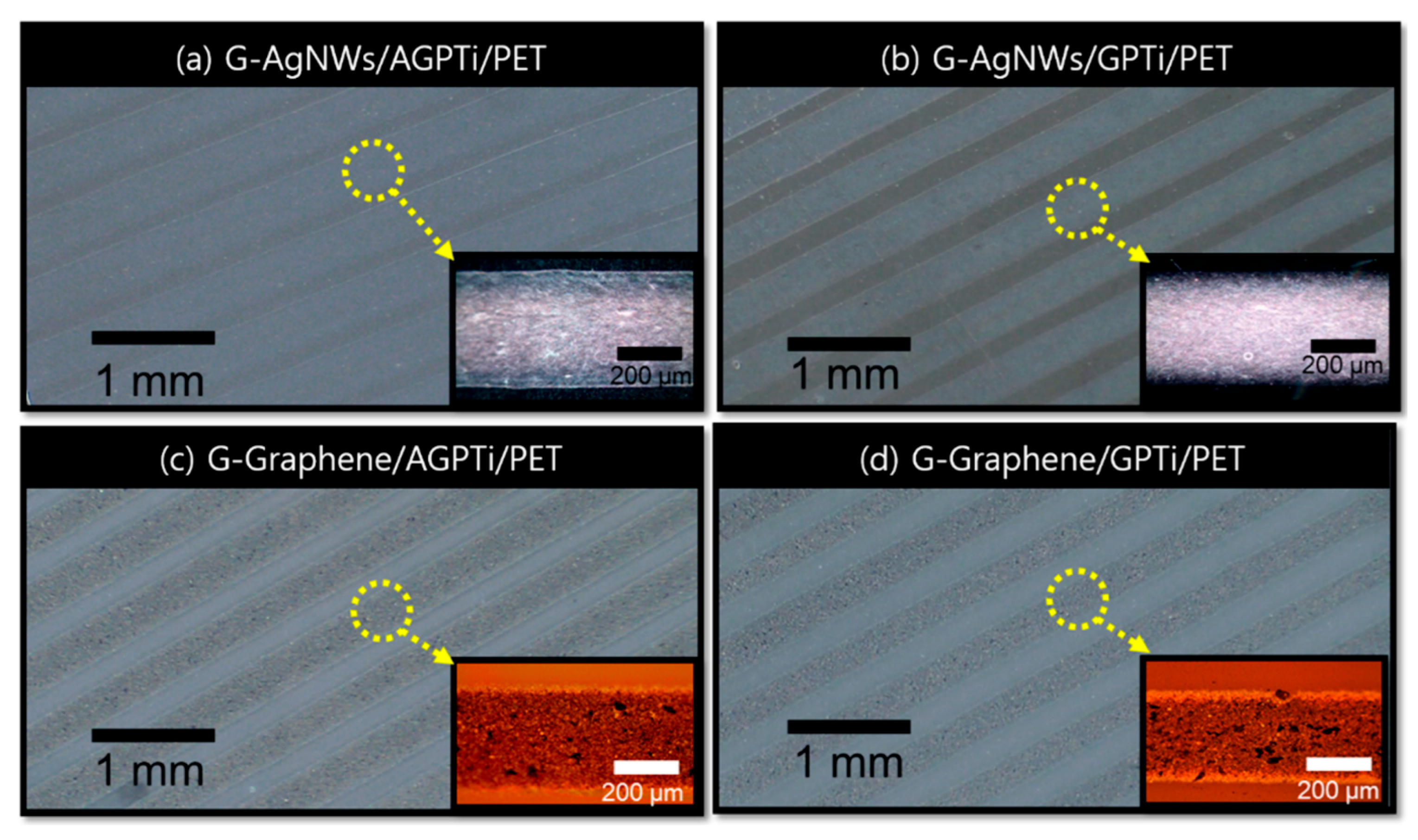
Ag nanowire ink for gravure printing is prepared by dispersing Ag nanowires in a solution along with suitable binders and solvents. The viscosity, surface tension, and other rheological properties of the ink must be optimized to achieve good transfer and pattern formation during printing. In addition, the use of stabilizing agents in the ink is essential to prevent nanowire agglomeration and maintain a stable dispersion for uniform printing. Li et al. fabricated Ag nanowire layers on glass substrates through gravure printing (Figure 13) [76]. They used an organic–inorganic nanohybrid ink prepared by incorporating an alkoxysilane-functionalized amphiphilic polymer precursor into a SiO2–TiO2 hybrid network (denoted as AGPTi) [76]. The gravure-printed Ag nanowire layers had uniform line widths of 490 ± 15 and 470 ± 12 µm, as well as excellent mechanical stability after 1000 bending cycles. Postprinting treatments such as thermal annealing or chemical treatments are often employed to enhance the conductivity and adhesion of Ag nanowire electrodes [71,72,73,74]. These treatments remove any residual binders and improve the interconnections between the nanowires, ultimately optimizing the electrical performance of the printed electrodes.
The transparency and conductivity of Ag nanowires make them well suited for use in optoelectronic devices, and the scalability of gravure printing is ideal for large-scale production [71,72,73,74]. Gravure printing is also versatile in terms of substrate compatibility, enabling the deposition of Ag nanowire electrodes on a wide range of materials, including flexible and transparent substrates. Consequently, the gravure printing of Ag nanowire electrodes is a promising technique for producing conductive patterns, including electrodes, on various substrates. Current research in this area is focused on maintaining ink stability, optimizing printing parameters, and ensuring the long-term stability of printed patterns. Future directions may involve the exploration of novel ink formulations, advances in printing cylinder technologies, and the development of in-line monitoring systems to enhance the precision and reproducibility of the printing process [71,72,73,74]. The ongoing exploration and refinement of Ag nanowire gravure printing in the field of printed electronics will contribute to the advancement of technologies that rely on high-performance, cost-effective, and scalable conductive patterns.
3. Additional Considerations for Ag Nanowire Layer Formation
There are several additional considerations for Ag nanowire layer formation. First, the choice of flexible polymeric substrate, like PET [77,78] or polyethylene naphthalate (PEN) [79,80], significantly impacts the mechanical, thermal, and adhesion properties of the prepared film. Recent advancements in coating techniques offer the possibility of tailoring these properties for specific applications, such as achieving mechanical flexibility for applications involving bending or stretching. Second, postcoating treatments such as drying and annealing are highly effective for enhancing the electrical conductivity and mechanical performance of a prepared film [14,15,20,30,31]. Researchers are continuously optimizing these treatments to improve film characteristics, including the morphology and Ag nanowire orientation. Advanced characterization techniques, including electrical conductivity measurements; optical transmittance analyses; and structural evaluations using scanning electron microscopy and atomic force microscopy, provide crucial insights for refining and optimizing post-fabrication processes [4,74,75,81]. Finally, the scalability of coating methods significantly influences their suitability for different applications [1,82,83,84,85,86]. R2R coating offers excellent scalability for mass production, whereas inkjet printing and spray coating offer advantages in terms of speed and efficiency.
Ag nanowire-coated films have diverse applications in flexible electronics, touchscreens, and solar cells. The exceptional properties of Ag nanowire-coated films, including transparency, flexibility, and conductivity, position them as essential components in the rapidly evolving field of flexible and transparent electronics.
Researchers are also actively exploring alternative materials and sustainable fabrication techniques, aiming to integrate these innovations with emerging technologies. This pursuit is driven by challenges including cost-effectiveness, scalability, and achieving uniformity over large areas. The complex interplay between coating methods, substrate choices, post-treatment processes, and characterization techniques should be more closely explored in future research to unlock new applications and breakthroughs in the field of transparent conductive films on flexible polymeric substrates.
4. Summary
Ag nanowire electrodes present a compelling alternative to traditional ITO electrodes for optoelectronic applications owing to their remarkable conductivity, flexibility, and transparency. This review explores recent trends in Ag nanowire electrode coating technologies. There are diverse coating methods for depositing Ag nanowires on flexible polymeric substrates, each with unique advantages for specific applications and production scales, as well as distinct challenges. Future research on these techniques will result in greater precision, uniformity, and substrate compatibility. The evolution of the field of Ag nanowire electrodes hinges on the development of these coating methods to meet the rapidly changing needs of diverse and advancing technologies.
Author Contributions
B.H. prepared the manuscript. H.H. and N.Q. revised the manuscript. All authors have read and agreed to the published version of the manuscript.
Funding
This research was supported by the GRDC (Global Research Development Center) Cooperative Hub Program through the National Research Foundation of Korea, funded by the Ministry of Science and ICT (MSIT) (RS-2023-00257595).
Data Availability Statement
Data sharing is not applicable.
Conflicts of Interest
The authors declare that they have no competing interests.
References
- Ahn, Y.; Jeong, Y.; Lee, Y. Improved Thermal Oxidation Stability of Solution-Processable Silver Nanowire Transparent Electrode by Reduced Graphene Oxide. ACS Appl. Mater. Interfaces 2012, 4, 6410–6414. [Google Scholar] [CrossRef]
- Bai, S.; Guo, X.; Chen, T.; Zhang, Y.; Zhang, X.; Yang, H.; Zhao, X. Solution processed fabrication of silver nanowire-MXene@PEDOT: PSS flexible transparent electrodes for flexible organic light-emitting diodes. Compos. Part A Appl. Sci. Manuf. 2020, 139, 106088. [Google Scholar] [CrossRef]
- Bhadra, R.; Jana, T.; Mitra, A.; Sahoo, P. Effect of CNT radius on flattening contact behaviour of CNT-Al nanocomposite: A numerical approch. Rep. Mech. Eng. 2023, 4, 121–130. [Google Scholar] [CrossRef]
- Basarir, F.; Madani, Z.; Vapaavuori, J. Recent Advances in Silver Nanowire Based Flexible Capacitive Pressure Sensors: From Structure, Fabrication to Emerging Applications. Adv. Mater. Interfaces 2022, 9, 2200866. [Google Scholar] [CrossRef]
- Bobinger, M.; Hinterleuthner, S.; Becherer, M.; Keddis, S.; Schwesinger, N.; Lugli, P. Energy harvesting from ambient light using PVDF with highly conductive and transparent silver nanowire/PEDOT:PSS hybride electrodes. In Proceedings of the 2017 IEEE 17th International Conference on Nanotechnology (IEEE-NANO), Pittsburgh, PA, USA, 25–28 July 2017; pp. 426–429. [Google Scholar]
- Hwang, B.; Han, Y.; Matteini, P. Bending Fatigue Behavior of Ag Nanowire/Cu Thin-Film Hybrid Interconnects for Wearable Electronics. Facta Univ. Ser. Mech. Eng. 2022, 20, 553–560. [Google Scholar] [CrossRef]
- Milić, P.; Marinković, D.; Klinge, S.; Cojbašić, Ž. Reissner-Mindlin Based Isogeometric Finite Element Formulation for Piezoelectric Active Laminated Shells. Teh. Vjesn. 2023, 30, 416–425. [Google Scholar] [CrossRef]
- Milić, P.; Marinković, D.; Ćojbašić, Ž. Geometrically Nonlinear Analysis of Piezoelectric Active Laminated Shells by Means of Isogeometric Fe Formulation. Facta Univ. Ser. Mech. Eng. 2023. online first. [Google Scholar] [CrossRef]
- Bobinger, M.; Keddis, S.; Hinterleuthner, S.; Becherer, M.; Kluge, F.; Schwesinger, N.; Salmerón, J.F.; Lugli, P.; Rivadeneyra, A. Light and Pressure Sensors Based on PVDF with Sprayed and Transparent Electrodes for Self-Powered Wireless Sensor Nodes. IEEE Sens. J. 2019, 19, 1114–1126. [Google Scholar] [CrossRef]
- Ayham, N.G.; Zuheir Fadhel, E.; Hashem Abbud, L. Investigation of the mechanical properties of nanocomposites with multi-wall carbon nanotube reinforcement and carbon fiber/epoxy. Rep. Mech. Eng. 2023, 4, 153–160. [Google Scholar] [CrossRef]
- Chen, S.; Song, L.; Tao, Z.; Shao, X.; Huang, Y.; Cui, Q.; Guo, X. Neutral-pH PEDOT:PSS as over-coating layer for stable silver nanowire flexible transparent conductive films. Org. Electron. 2014, 15, 3654–3659. [Google Scholar] [CrossRef]
- Cho, S.; Kang, S.; Pandya, A.; Shanker, R.; Khan, Z.; Lee, Y.; Park, J.; Craig, S.L.; Ko, H. Large-Area Cross-Aligned Silver Nanowire Electrodes for Flexible, Transparent, and Force-Sensitive Mechanochromic Touch Screens. ACS Nano 2017, 11, 4346–4357. [Google Scholar] [CrossRef] [PubMed]
- Choi, J.H.; Lee, K.Y.; Kim, S.W. Ultra-bendable and durable Graphene–Urethane composite/silver nanowire film for flexible transparent electrodes and electromagnetic-interference shielding. Compos. Part B Eng. 2019, 177, 107406. [Google Scholar] [CrossRef]
- Choi, Y.; Kim, C.S.; Jo, S. Spray Deposition of Ag Nanowire–Graphene Oxide Hybrid Electrodes for Flexible Polymer–Dispersed Liquid Crystal Displays. Materials 2018, 11, 2231. [Google Scholar] [CrossRef] [PubMed]
- Fang, F.; Huang, G.-W.; Xiao, H.-M.; Li, Y.-Q.; Hu, N.; Fu, S.-Y. Largely enhanced electrical conductivity of layer-structured silver nanowire/polyimide composite films by polyaniline. Compos. Sci. Technol. 2018, 156, 144–150. [Google Scholar] [CrossRef]
- Hwang, B.; Lund, A.; Tian, Y.; Darabi, S.; Müller, C. Machine-Washable Conductive Silk Yarns with a Composite Coating of Ag Nanowires and PEDOT:PSS. ACS Appl. Mater. Interfaces 2020, 12, 27537–27544. [Google Scholar] [CrossRef] [PubMed]
- Kim, H.; Qaiser, N.; Hwang, B. Electro-Mechanical Response of Stretchable PDMS Composites with a Hybrid Filler System. Facta Univ. Ser. Mech. Eng. 2023, 21, 51–61. [Google Scholar] [CrossRef]
- Ghosh, D.S.; Chen, T.L.; Mkhitaryan, V.; Pruneri, V. Ultrathin Transparent Conductive Polyimide Foil Embedding Silver Nanowires. ACS Appl. Mater. Interfaces 2014, 6, 20943–20948. [Google Scholar] [CrossRef]
- Leroy, J.-E.; Popov, V.L. Stress tensor in the linear viscoelastic incompressible half-space beneath axisymmetric bodies in normal contact. Rep. Mech. Eng. 2023, 4, 310–316. [Google Scholar] [CrossRef]
- Ha, H.; Müller, S.; Baumann, R.-P.; Hwang, B. PeakForce Quantitative Nanomechanical Mapping for Surface Energy Characterization on the Nanoscale: A Mini-Review. Facta Univ. Ser. Mech. Eng. 2023. online first. [Google Scholar] [CrossRef]
- Gao, D.; Zhao, P.; Liu, J.; Zhou, Y.; Lyu, B.; Ma, J.; Shao, L. Polyaniline/silver nanowire cotton fiber: A flexible electrode material for supercapacitor. Adv. Powder Technol. 2021, 32, 3954–3963. [Google Scholar] [CrossRef]
- Ha, H.; Amicucci, C.; Matteini, P.; Hwang, B. Mini review of synthesis strategies of silver nanowires and their applications. Colloid Interface Sci. Commun. 2022, 50, 100663. [Google Scholar] [CrossRef]
- Bzinkowski, D.; Ryba, T.; Siemiatkowski, Z.; Rucki, M. Real-time monitoring of the rubber belt tension in an industrial conveyor. Rep. Mech. Eng. 2022, 3, 1–10. [Google Scholar] [CrossRef]
- Ha, H.; Qaiser, N.; Yun, T.G.; Cheong, J.Y.; Lim, S.; Hwang, B. Sensing Mechanism and Application of Mechanical Strain Sensor: A Mini-Review. Facta Univ. Ser. Mech. Eng. 2023, 21, 751–772. [Google Scholar] [CrossRef]
- Seo, Y.; Hwang, B. Mulberry-paper-based composites for flexible electronics and energy storage devices. Cellulose 2019, 26, 8867–8875. [Google Scholar] [CrossRef]
- Shah, K.W.; Xiong, T. Multifunctional Metallic Nanowires in Advanced Building Applications. Materials 2019, 12, 1731. [Google Scholar] [CrossRef]
- Nam, V.B.; Lee, D. Copper Nanowires and Their Applications for Flexible, Transparent Conducting Films: A Review. Nanomaterials 2016, 6, 47. [Google Scholar] [CrossRef]
- Xiong, W.; Liu, H.; Chen, Y.; Zheng, M.; Zhao, Y.; Kong, X.; Wang, Y.; Zhang, X.; Kong, X.; Wang, P.; et al. Highly Conductive, Air-Stable Silver Nanowire@Iongel Composite Films toward Flexible Transparent Electrodes. Adv. Mater. 2016, 28, 7167–7172. [Google Scholar] [CrossRef]
- Lian, L.; Dong, D.; Feng, D.; He, G. Low roughness silver nanowire flexible transparent electrode by low temperature solution-processing for organic light emitting diodes. Org. Electron. 2017, 49, 9–18. [Google Scholar] [CrossRef]
- Luo, M.; Liu, Y.; Huang, W.; Qiao, W.; Zhou, Y.; Ye, Y.; Chen, L.-S. Towards Flexible Transparent Electrodes Based on Carbon and Metallic Materials. Micromachines 2017, 8, 12. [Google Scholar] [CrossRef]
- Morales-Masis, M.; De Wolf, S.; Woods-Robinson, R.; Ager, J.W.; Ballif, C. Transparent Electrodes for Efficient Optoelectronics. Adv. Electron. Mater. 2017, 3, 1600529. [Google Scholar] [CrossRef]
- Hwang, B.; Yun, T.G. Stretchable and patchable composite electrode with trimethylolpropane formal acrylate-based polymer. Compos. Part B Eng. 2019, 163, 185–192. [Google Scholar] [CrossRef]
- Xie, H.; Yang, X.; Du, D.; Zhao, Y.; Wang, Y. Flexible Transparent Conductive Film Based on Random Networks of Silver Nanowires. Micromachines 2018, 9, 295. [Google Scholar] [CrossRef]
- He, X.; Shen, G.; Xu, R.; Yang, W.; Zhang, C.; Liu, Z.; Chen, B.; Liu, J.; Song, M. Hexagonal and Square Patterned Silver Nanowires/PEDOT:PSS Composite Grids by Screen Printing for Uniformly Transparent Heaters. Polymers 2019, 11, 468. [Google Scholar] [CrossRef]
- Khadtare, S.; Ko, E.J.; Kim, Y.H.; Lee, H.S.; Moon, D.K. A flexible piezoelectric nanogenerator using conducting polymer and silver nanowire hybrid electrodes for its application in real-time muscular monitoring system. Sens. Actuators A Phys. 2019, 299, 111575. [Google Scholar] [CrossRef]
- Zhu, Z.; Wang, X.; Li, D.; Yu, H.; Li, X.; Guo, F. Solvent Welding-Based Methods Gently and Effectively Enhance the Conductivity of a Silver Nanowire Network. Nanomaterials 2023, 13, 2865. [Google Scholar] [CrossRef]
- Sohn, H.; Park, C.; Oh, J.-M.; Kang, S.W.; Kim, M.-J. Silver Nanowire Networks: Mechano-Electric Properties and Applications. Materials 2019, 12, 2526. [Google Scholar] [CrossRef]
- Gorji, M.; Mazinani, S.; Faramarzi, A.-R.; Ghadimi, S.; Kalaee, M.; Sadeghianmaryan, A.; Wilson, L.D. Coating Cellulosic Material with Ag Nanowires to Fabricate Wearable IR-Reflective Device for Personal Thermal Management: The Role of Coating Method and Loading Level. Molecules 2021, 26, 3570. [Google Scholar] [CrossRef]
- Kim, J.-H.; Ma, J.; Jo, S.; Lee, S.; Kim, C.S. Enhancement of Antibacterial Performance of Silver Nanowire Transparent Film by Post-Heat Treatment. Nanomaterials 2020, 10, 938. [Google Scholar] [CrossRef]
- Jin, I.S.; Lee, H.D.; Hong, S.I.; Lee, W.; Jung, J.W. Facile Post Treatment of Ag Nanowire/Polymer Composites for Flexible Transparent Electrodes and Thin Film Heaters. Polymers 2021, 13, 586. [Google Scholar] [CrossRef]
- Kumar, A.; Shaikh, M.O.; Chuang, C.-H. Silver Nanowire Synthesis and Strategies for Fabricating Transparent Conducting Electrodes. Nanomaterials 2021, 11, 693. [Google Scholar] [CrossRef]
- Choi, J.H.; Shin, M.G.; Jung, Y.; Kim, D.H.; Ko, J.S. Fabrication and Performance Evaluation of Highly Sensitive Flexible Strain Sensors with Aligned Silver Nanowires. Micromachines 2020, 11, 156. [Google Scholar] [CrossRef]
- Zeng, F.; Zheng, Y.; Wei, Y.; Li, H.; Wang, Q.; Shi, J.; Wang, Y.; Hong, X. Multifunctional Silver Nanowire Fabric Reinforced by Hot Pressing for Electromagnetic Interference Shielding, Electric Heating, and Sensing. Polymers 2023, 15, 4258. [Google Scholar] [CrossRef]
- Lee, S.H.; Lee, S. Cantilever Type Acceleration Sensors Made by Roll-to-Roll Slot-Die Coating. Sensors 2020, 20, 3748. [Google Scholar] [CrossRef]
- Liu, C.; Zhang, X.; Shan, J.; Li, Z.; Guo, X.; Zhao, X.; Yang, H. Large-Scale Preparation of Silver Nanowire-Based Flexible Transparent Film Heaters by Slot-Die Coating. Materials 2022, 15, 2634. [Google Scholar] [CrossRef]
- Kim, Y.J.; Kim, G.; Kim, H.-K. Study of Brush-Painted Ag Nanowire Network on Flexible Invar Metal Substrate for Curved Thin Film Heater. Metals 2019, 9, 1073. [Google Scholar] [CrossRef]
- Wu, X.; Zhou, Z.; Wang, Y.; Li, J. Syntheses of Silver Nanowires Ink and Printable Flexible Transparent Conductive Film: A Review. Coatings 2020, 10, 865. [Google Scholar] [CrossRef]
- Jeong, H.; Lee, J.H.; Song, J.-Y.; Ghani, F.; Lee, D. Continuous Patterning of Silver Nanowire-Polyvinylpyrrolidone Composite Transparent Conductive Film by a Roll-to-Roll Selective Calendering Process. Nanomaterials 2023, 13, 32. [Google Scholar] [CrossRef]
- Lim, S.-H.; Kim, H.-K. Thermal Profiles of Carbon Fiber Based Anisotropic Thin-Films: An Emerging Heat Management Solution for High-Current Flow Electrocatalysis and Electrochemical Applications. Catalysts 2020, 10, 1172. [Google Scholar] [CrossRef]
- Xu, H.; Liu, P.; Huang, B.; Jiang, X.; Gao, Q.; Liu, L. Preparation of Double-Layer Crossed Silver Nanowire Film and Its Application to OLED. Coatings 2022, 12, 26. [Google Scholar] [CrossRef]
- Camic, B.T.; Jeong, H.I.; Aslan, M.H.; Kosemen, A.; Kim, S.; Choi, H.; Basarir, F.; Lee, B.R. Preparation of Transparent Conductive Electrode via Layer-By-Layer Deposition of Silver Nanowires and Its Application in Organic Photovoltaic Device. Nanomaterials 2020, 10, 46. [Google Scholar] [CrossRef]
- Heo, S.W. Ultra-Flexible Organic Photovoltaics with Nanograting Patterns Based on CYTOP/Ag Nanowires Substrate. Nanomaterials 2020, 10, 2185. [Google Scholar] [CrossRef]
- Li, X.; Zhou, J.; Yan, D.; Peng, Y.; Wang, Y.; Zhou, Q.; Wang, K. Effects of Concentration and Spin Speed on the Optical and Electrical Properties of Silver Nanowire Transparent Electrodes. Materials 2021, 14, 2219. [Google Scholar] [CrossRef]
- Zhang, J.; Zhu, X.; Xu, J.; Xu, R.; Yang, H.; Kan, C. Comparative Study on Preparation Methods for Transparent Conductive Films Based on Silver Nanowires. Molecules 2022, 27, 8907. [Google Scholar] [CrossRef]
- Lee, G.; Kim, H.; Lee, S.B.; Kim, D.; Lee, E.; Lee, S.K.; Lee, S.G. Tailored Uniaxial Alignment of Nanowires Based on Off-Center Spin-Coating for Flexible and Transparent Field-Effect Transistors. Nanomaterials 2022, 12, 1116. [Google Scholar] [CrossRef]
- Wang, J.; Yu, J.; Bai, D.; Li, Z.; Liu, H.; Li, Y.; Chen, S.; Cheng, J.; Li, L. Biodegradable, Flexible, and Transparent Conducting Silver Nanowires/Polylactide Film with High Performance for Optoelectronic Devices. Polymers 2020, 12, 604. [Google Scholar] [CrossRef]
- Yang, X.; Du, D.; Wang, Y.; Zhao, Y. Silver Nanowires Inks for Flexible Circuit on Photographic Paper Substrate. Micromachines 2019, 10, 22. [Google Scholar] [CrossRef]
- Kong, J.; Wang, Y.; Wu, Y.; Zhang, L.; Gong, M.; Lin, X.; Wang, D. Toward High-Energy-Density Aqueous Lithium-Ion Batteries Using Silver Nanowires as Current Collectors. Molecules 2022, 27, 8207. [Google Scholar] [CrossRef]
- Yoon, H.; Matteini, P.; Hwang, B. Effect of the Blade-Coating Conditions on the Electrical and Optical Properties of Transparent Ag Nanowire Electrodes. Micromachines 2023, 14, 114. [Google Scholar] [CrossRef]
- Du, D.; Yang, X.; Yang, Y.; Zhao, Y.; Wang, Y. Silver Nanowire Ink for Flexible Circuit on Textiles. Micromachines 2019, 10, 42. [Google Scholar] [CrossRef]
- Wang, S.; Wu, X.; Lu, J.; Luo, Z.; Xie, H.; Zhang, X.; Lin, K.; Wang, Y. Inkjet-Printed Silver Nanowire Ink for Flexible Transparent Conductive Film Applications. Nanomaterials 2022, 12, 842. [Google Scholar] [CrossRef]
- Wang, Y.; Wu, X.; Wang, K.; Lin, K.; Xie, H.; Zhang, X.; Li, J. Novel Insights into Inkjet Printed Silver Nanowires Flexible Transparent Conductive Films. Int. J. Mol. Sci. 2021, 22, 7719. [Google Scholar] [CrossRef]
- Ke, S.-H.; Xue, Q.-W.; Pang, C.-Y.; Guo, P.-W.; Yao, W.-J.; Zhu, H.-P.; Wu, W. Printing the Ultra-Long Ag Nanowires Inks onto the Flexible Textile Substrate for Stretchable Electronics. Nanomaterials 2019, 9, 686. [Google Scholar] [CrossRef]
- Wu, X.; Wang, S.; Luo, Z.; Lu, J.; Lin, K.; Xie, H.; Wang, Y.; Li, J.-Z. Inkjet Printing of Flexible Transparent Conductive Films with Silver Nanowires Ink. Nanomaterials 2021, 11, 1571. [Google Scholar] [CrossRef]
- Reenaers, D.; Marchal, W.; Biesmans, I.; Nivelle, P.; D’Haen, J.; Deferme, W. Layer Morphology and Ink Compatibility of Silver Nanoparticle Inkjet Inks for Near-Infrared Sintering. Nanomaterials 2020, 10, 892. [Google Scholar] [CrossRef]
- Wang, J.; Lou, Y.; Wang, B.; Sun, Q.; Zhou, M.; Li, X. Highly Sensitive, Breathable, and Flexible Pressure Sensor Based on Electrospun Membrane with Assistance of AgNW/TPU as Composite Dielectric Layer. Sensors 2020, 20, 2459. [Google Scholar] [CrossRef]
- Li, B.; Xu, C.; Zheng, J.; Xu, C. Sensitivity of Pressure Sensors Enhanced by Doping Silver Nanowires. Sensors 2014, 14, 9889–9899. [Google Scholar] [CrossRef]
- Chen, M.; Wang, Z.; Zheng, Y.; Zhang, Q.; He, B.; Yang, J.; Qi, M.; Wei, L. Flexible Tactile Sensor Based on Patterned Ag-Nanofiber Electrodes through Electrospinning. Sensors 2021, 21, 2413. [Google Scholar] [CrossRef]
- Xiao, J.; Li, Y.; Wang, J.; Xu, Y.; Zhang, G.; Leng, C. Preparation and Antibiosis Investigation of Kaolinite Nanotubes and Silver Nanowires Co-Doped Electrospinning-Silk Fibroin/Gelatin Porous Fiber Films. Metals 2023, 13, 745. [Google Scholar] [CrossRef]
- Wang, X.; Sun, F.; Yin, G.; Wang, Y.; Liu, B.; Dong, M. Tactile-Sensing Based on Flexible PVDF Nanofibers via Electrospinning: A Review. Sensors 2018, 18, 330. [Google Scholar] [CrossRef]
- Park, S.; Kim, H.; Kim, J.-H.; Yeo, W.-H. Advanced Nanomaterials, Printing Processes, and Applications for Flexible Hybrid Electronics. Materials 2020, 13, 3587. [Google Scholar] [CrossRef]
- Yang, J.; Zeng, W.; Li, Y.; Yi, Z.; Zhou, G. Fabrication of Screen Printing-Based AgNWs Flexible Transparent Conductive Film with High Stability. Micromachines 2020, 11, 1027. [Google Scholar] [CrossRef]
- Garcia, A.J.L.; Sico, G.; Montanino, M.; Defoor, V.; Pusty, M.; Mescot, X.; Loffredo, F.; Villani, F.; Nenna, G.; Ardila, G. Low-Temperature Growth of ZnO Nanowires from Gravure-Printed ZnO Nanoparticle Seed Layers for Flexible Piezoelectric Devices. Nanomaterials 2021, 11, 1430. [Google Scholar] [CrossRef]
- Giasafaki, D.; Mitzithra, C.; Belessi, V.; Filippakopoulou, T.; Koutsioukis, A.; Georgakilas, V.; Charalambopoulou, G.; Steriotis, T. Graphene-Based Composites with Silver Nanowires for Electronic Applications. Nanomaterials 2022, 12, 3443. [Google Scholar] [CrossRef]
- Garcia, A.J.L.; Jalabert, T.; Pusty, M.; Defoor, V.; Mescot, X.; Montanino, M.; Sico, G.; Loffredo, F.; Villani, F.; Nenna, G.; et al. Size and Semiconducting Effects on the Piezoelectric Performances of ZnO Nanowires Grown onto Gravure-Printed Seed Layers on Flexible Substrates. Nanoenergy Adv. 2022, 2, 197–209. [Google Scholar] [CrossRef]
- Li, X.; Kim, N.; Youn, S.; An, T.K.; Kim, J.; Lim, S.; Kim, S.H. Sol–Gel-Processed Organic–Inorganic Hybrid for Flexible Conductive Substrates Based on Gravure-Printed Silver Nanowires and Graphene. Polymers 2019, 11, 158. [Google Scholar] [CrossRef]
- Huang, C.-H.; Wang, Y.-Y.; Lu, T.-H.; Li, Y.-C. Flexible Transparent Electrode of Hybrid Ag-Nanowire/Reduced-Graphene-Oxide Thin Film on PET Substrate Prepared Using H2/Ar Low-Damage Plasma. Polymers 2017, 9, 28. [Google Scholar] [CrossRef] [PubMed]
- Xu, L.; Weng, W.-C.; Yeh, Y.-C. Continuous Wave Laser Nanowelding Process of Ag Nanowires on Flexible Polymer Substrates. Nanomaterials 2021, 11, 2511. [Google Scholar] [CrossRef] [PubMed]
- Zacharatos, F.; Karvounis, P.; Theodorakos, I.; Hatziapostolou, A.; Zergioti, I. Single Step Laser Transfer and Laser Curing of Ag NanoWires: A Digital Process for the Fabrication of Flexible and Transparent Microelectrodes. Materials 2018, 11, 1036. [Google Scholar] [CrossRef] [PubMed]
- Oh, J.; Wen, L.; Tak, H.; Kim, H.; Kim, G.; Hong, J.; Chang, W.; Kim, D.; Yeom, G. Radio Frequency Induction Welding of Silver Nanowire Networks for Transparent Heat Films. Materials 2021, 14, 4448. [Google Scholar] [CrossRef] [PubMed]
- Zhu, Y.; Li, X.; Xu, Y.; Wu, L.; Yu, A.; Lai, G.; Wei, Q.; Chi, H.; Jiang, N.; Fu, L.; et al. Intertwined Carbon Nanotubes and Ag Nanowires Constructed by Simple Solution Blending as Sensitive and Stable Chloramphenicol Sensors. Sensors 2021, 21, 1220. [Google Scholar] [CrossRef] [PubMed]
- Pang, S.; Hernandez, Y.; Feng, X.; Müllen, K. Graphene as Transparent Electrode Material for Organic Electronics. Adv. Mater. 2011, 23, 2779–2795. [Google Scholar] [CrossRef] [PubMed]
- Tokuno, T.; Nogi, M.; Karakawa, M.; Jiu, J.; Nge, T.T.; Aso, Y.; Suganuma, K. Fabrication of silver nanowire transparent electrodes at room temperature. Nano Res. 2011, 4, 1215–1222. [Google Scholar] [CrossRef]
- Hu, W.; Niu, X.; Zhao, R.; Pei, Q. Elastomeric transparent capacitive sensors based on an interpenetrating composite of silver nanowires and polyurethane. Appl. Phys. Lett. 2013, 102, 083303. [Google Scholar] [CrossRef]
- Kim, A.; Won, Y.; Woo, K.; Kim, C.-H.; Moon, J. Highly Transparent Low Resistance ZnO/Ag Nanowire/ZnO Composite Electrode for Thin Film Solar Cells. ACS Nano 2013, 7, 1081–1091. [Google Scholar] [CrossRef] [PubMed]
- Lee, D.; Lee, H.; Ahn, Y.; Jeong, Y.; Lee, D.-Y.; Lee, Y. Highly stable and flexible silver nanowire–graphene hybrid transparent conducting electrodes for emerging optoelectronic devices. Nanoscale 2013, 5, 7750–7755. [Google Scholar] [CrossRef] [PubMed]
Figure 1.
Synthesis, characterization, and applications of Ag nanowires [26]. Reproduced from Ref. [26] under the Creative Commons Attribution 4.0 International (CC BY 4.0) License.

Figure 2.
Ag nanowire layer formation using spray coating [36]. (A) Schematic of Ag nanowire synthesis with PVP (red lines) and camphorquinone (CQ; blue dots) capping; (B) fabrication of Ag nanowire network via spray coating; (C) solvent welding and corresponding state of Ag nanowire junctions; (D) solvent-based plasmonic welding; and (E) combined solvent-based plasmonic and Joule-heating welding. Reproduced from Ref. [36] under the Creative Commons Attribution 4.0 International (CC BY 4.0) License.

Figure 3.
Formation of Ag nanowire (AgNW) layers using dip coating. Schematic diagram of dip-coating and hot-pressing processes for embedding Ag nanowires into PET fabric [43]. Reproduced from Ref. [43] under the Creative Commons Attribution 4.0 International (CC BY 4.0) License.

Figure 4.
Comparison of the degree of alignment of silver nanowires [42]: (a) SEM image of unaligned silver nanowires; (b) SEM image of silver nanowires aligned using temperature-controlled dip coating process; (c) SEM image of silver nanowires transferred to PDMS; (d) analysis of degree of alignment of unaligned silver nanowires; (e) analysis of degree of alignment of silver nanowires aligned using temperature-controlled dip coating process; and (f) analysis of degree of alignment of transferred silver nanowires. Insets of (d–f) show the distribution of nanowires according to the angle, and the amount of silver nanowires is expressed in color. Reproduced from Ref. [42] under the Creative Commons Attribution 4.0 International (CC BY 4.0) License.

Figure 5.
R2R-processed continuous patterning by selective calendering: (a) schematic illustration of patterning via R2R manufacturing; (b) selective calendering mechanism of Ag nanowire-PVP transparent conductive film using an embossed pattern roll; (c) pressure-sensitive paper pressed by an embossed pattern roll; and (d) comparison of the resistance between the unpressed and pressed part in a single-line pattern. Reproduced from Ref. [48] under the Creative Commons Attribution 4.0 International (CC BY 4.0) License.

Figure 6.
(left) (a) aligned angle of carbon fiber to an imaginary perpendicular line—carbon fibers with aligned angle less than 45° are colored red, and above 45° are colored blue; (right) (a) overlaid colored surface FESEM image of carbon fiber thin film [49]. (left) (b) schematic of electron pathway is overlaid on FESEM image of CF thin film, in which majority of CFs are aligned perpendicular to direction of applied voltage (perpendicular CFTF); (right) (b) majority of CFs aligned parallel to direction of applied voltage (parallel CFTF) [49]. Reproduced from Ref. [49] under the Creative Commons Attribution 4.0 International (CC BY 4.0) License.

Figure 7.
Photographs of Ag nanowire-based films prepared through (a) Mayer rod coating, (b) spin coating, (c) spray coating, and (d) vacuum-filtration methods. Insets are corresponding diagrams of these four methods. Reproduced from Ref. [54] under the Creative Commons Attribution 4.0 International (CC BY 4.0) License.

Figure 8.
Schematic diagrams of the overall spin-coating processes and their effects upon NW alignment [55]: (a) the conventional spin-coating setup (i) and the proposed off-center spin-coating setup (ii) with inset polarized optical microscope images of the as-deposited Si nanowires; (b) the forces involved in the off-center spin-coating mechanism, including Inertial (centrifugal) Force I, due to centripetal acceleration (blue), Inertial Force II (red), due to tangential acceleration, and the resultant force (green); (c) the sequential influence of the resultant force upon the uniaxial alignment of the NWs that are in partial contact with the substrate surface. Reproduced from Ref. [55] under the Creative Commons Attribution 4.0 International (CC BY 4.0) License.

Figure 9.
Schematic of the coating process for the production of transparent Ag nanowire (AgNW) electrodes using a doctor-blade system: (a) applying an AgNW suspension, (b) blade coating, and (c) drying in an oven. Reproduced from Ref. [59] under the Creative Commons Attribution 4.0 International (CC BY 4.0) License.

Figure 10.
Schematic diagrams of Ag nanowire (AgNW)-based conductive ink fabrication and the inkjet printing process. A schematic of the deposited Ag nanowire flexible transparent conductive film is shown in the center. Reproduced from Ref. [64] under the Creative Commons Attribution 4.0 International (CC BY 4.0) License.

Figure 11.
Sintering at shorter distances results in lower sheet resistance and requires a smaller number of flashes [65] (A). The higher light intensity at shorter distances causes a higher surface roughness; it exponentially decreases with increasing sintering distance according to the decrease of light intensity. (Every datapoint consists of three corresponding samples, with every sample measured on two locations with the profilometer (line measurement); the error bars represent the standard deviation of each population). (B). The layer thickness decreases linearly when increasing the sintering distance for JS-A102A at a flashing intensity of 100% and a flash and cooling time of 2 s. (Each data point is representing the average of 8 to 12 measurements distributed over four to six different samples. The error bars represent the standard deviation of each population). (C). Reproduced from Ref. [65] under the Creative Commons Attribution 4.0 International (CC BY 4.0) License.

Figure 12.
Fabrication of nanofiber membrane-based flexible capacitive pressure sensor: (a,b) preparation of Ag nanowires (AgNWs); (c) preparation of spinning solution; (d) electrospinning process; and (e–g) assembly of sensors—electrode printing and ultrasonic welding. Reproduced from Ref. [66] under the Creative Commons Attribution 4.0 International (CC BY 4.0) License.

Figure 13.
Gravure-printed lines of Ag nanowires and graphene on AGPTi: (a) G-Ag nanowires/AGPTi/PET; (c) G-graphene/AGPTi/PET) and GPTi; (b) G-Ag nanowires/GPTi/PET; and (d) G-graphene/GPTi/PET), previously deposited on PET. Reproduced from Ref. [76] under the Creative Commons Attribution 4.0 International (CC BY 4.0) License.

Disclaimer/Publisher’s Note: The statements, opinions and data contained in all publications are solely those of the individual author(s) and contributor(s) and not of MDPI and/or the editor(s). MDPI and/or the editor(s) disclaim responsibility for any injury to people or property resulting from any ideas, methods, instructions or products referred to in the content. |
© 2024 by the authors. Licensee MDPI, Basel, Switzerland. This article is an open access article distributed under the terms and conditions of the Creative Commons Attribution (CC BY) license (https://creativecommons.org/licenses/by/4.0/).
Share and Cite
MDPI and ACS Style
Ha, H.; Qaiser, N.; Hwang, B. Introductory Overview of Layer Formation Techniques of Ag Nanowires on Flexible Polymeric Substrates. Inorganics 2024, 12, 65. https://0-doi-org.brum.beds.ac.uk/10.3390/inorganics12030065
AMA Style
Ha H, Qaiser N, Hwang B. Introductory Overview of Layer Formation Techniques of Ag Nanowires on Flexible Polymeric Substrates. Inorganics. 2024; 12(3):65. https://0-doi-org.brum.beds.ac.uk/10.3390/inorganics12030065
Chicago/Turabian StyleHa, Heebo, Nadeem Qaiser, and Byungil Hwang. 2024. "Introductory Overview of Layer Formation Techniques of Ag Nanowires on Flexible Polymeric Substrates" Inorganics 12, no. 3: 65. https://0-doi-org.brum.beds.ac.uk/10.3390/inorganics12030065
Note that from the first issue of 2016, this journal uses article numbers instead of page numbers. See further details here.