
Diamond as Insulation for Conductive Diamond—A Spotted Pattern Design for Miniaturized Disinfection Devices
 , , and
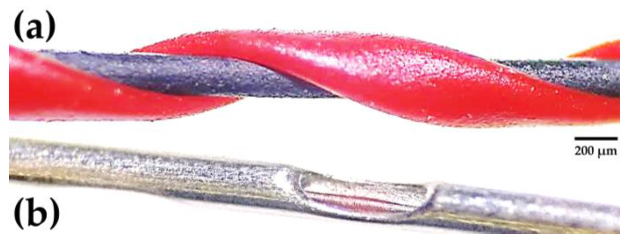
Abstract
:1. Introduction
2. Materials and Methods
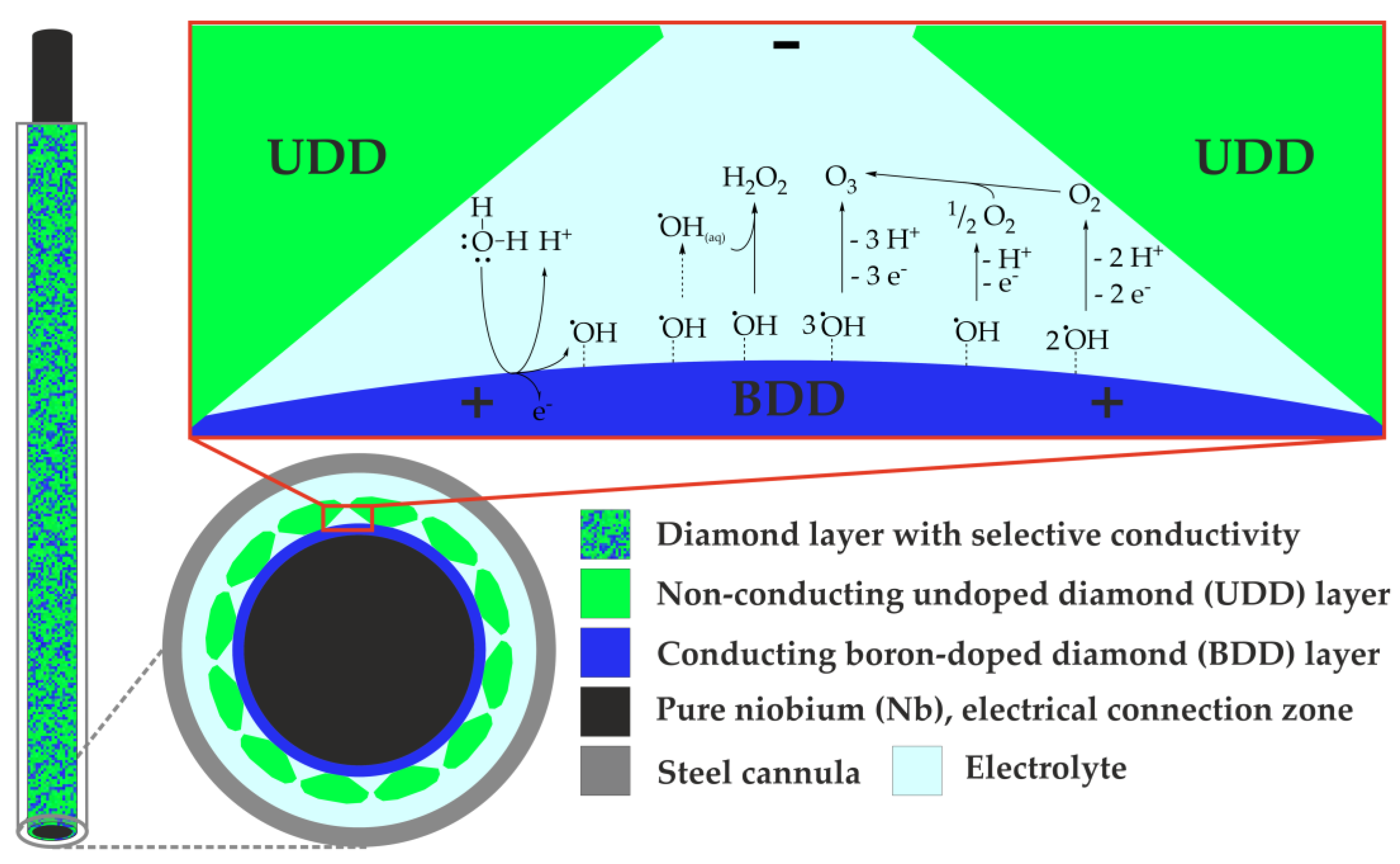
2.1. Conductive Diamond Coating of Niobium Wires
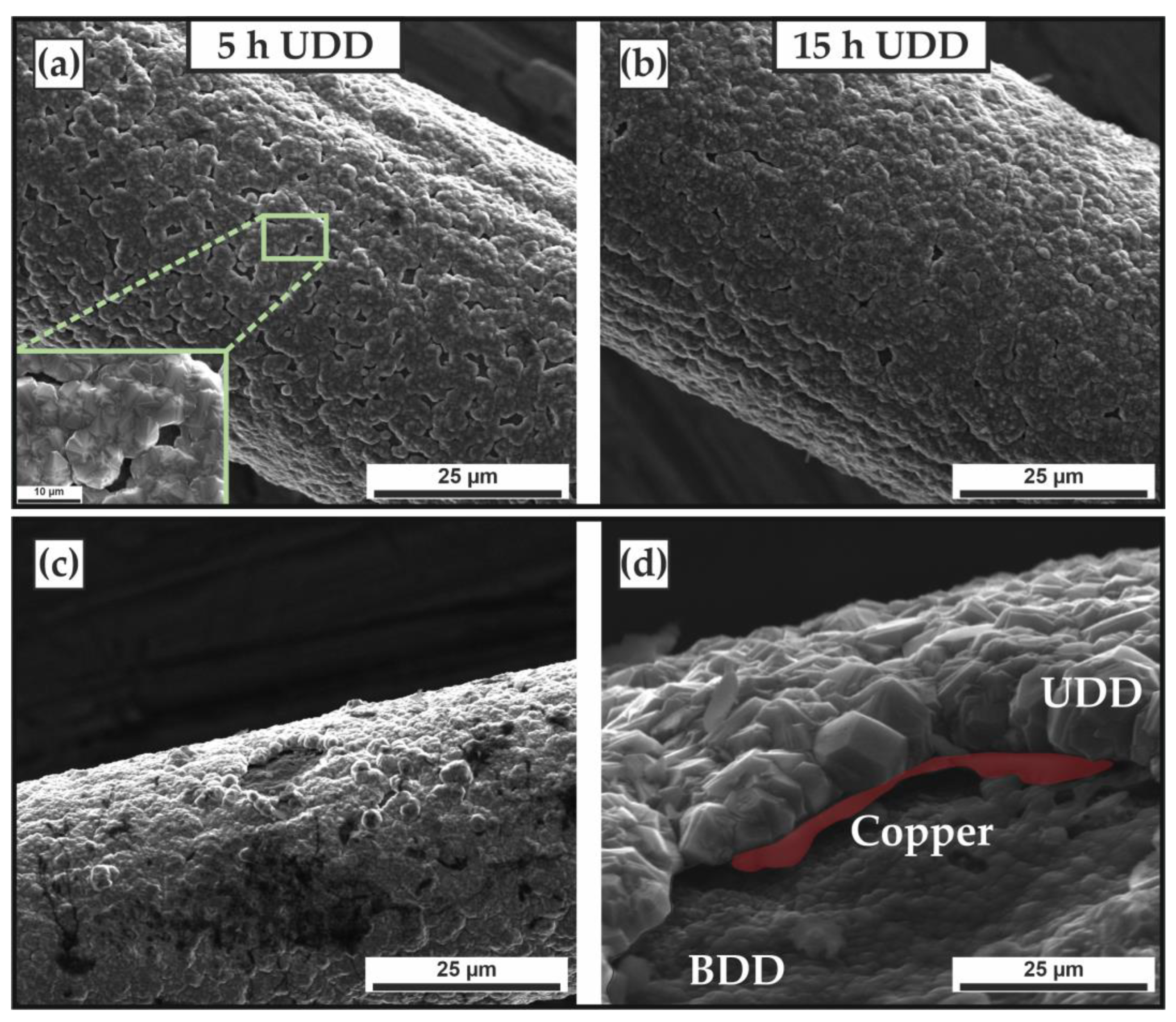
2.2. Spotted Copper Deposition (SCD) as Intermediate Layer
2.3. Non-Conductive Diamond Coating of BDD/Cu/Niobium Wires
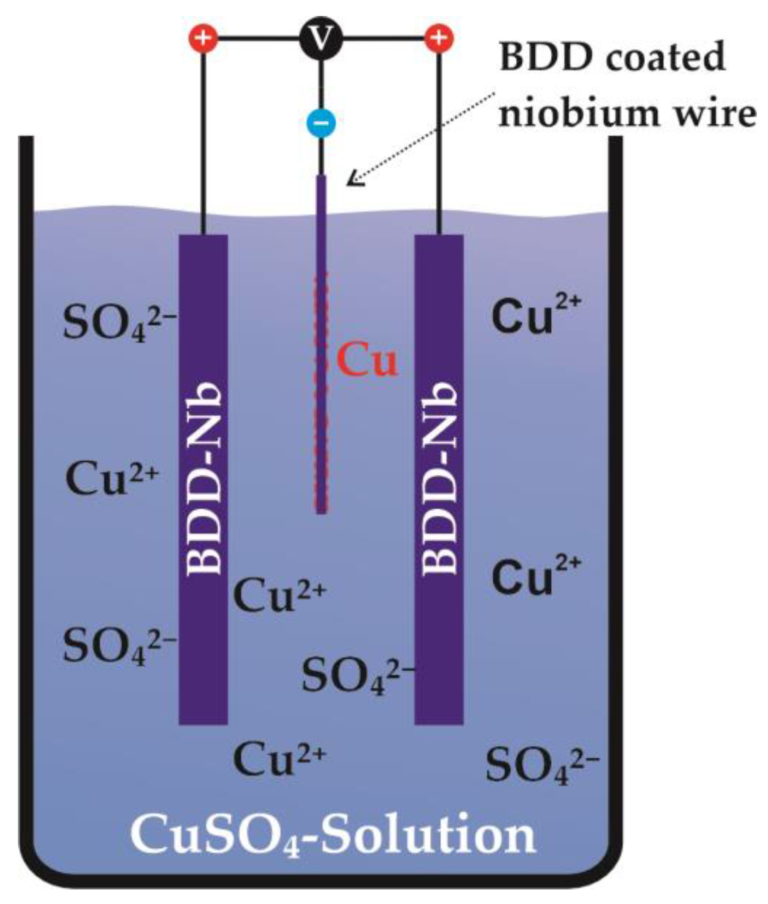
2.4. Electrochemical and Acidic Etching of Copper
2.5. Prototype Design and Manufacturing Process
2.6. Analysis of Oxidant Production
3. Results
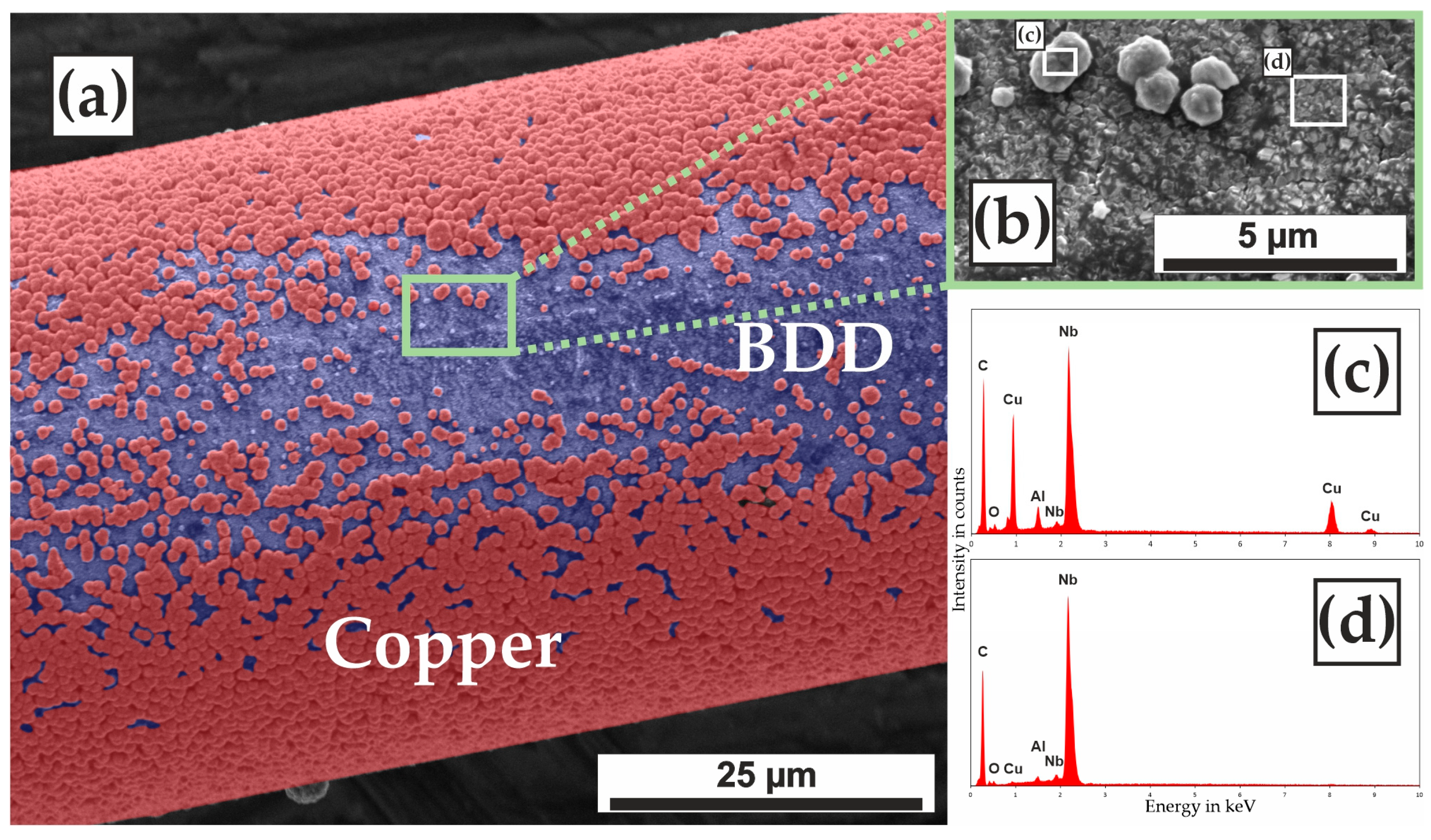
3.1. Electrochemical Deposition of Copper as Intermediate Layer
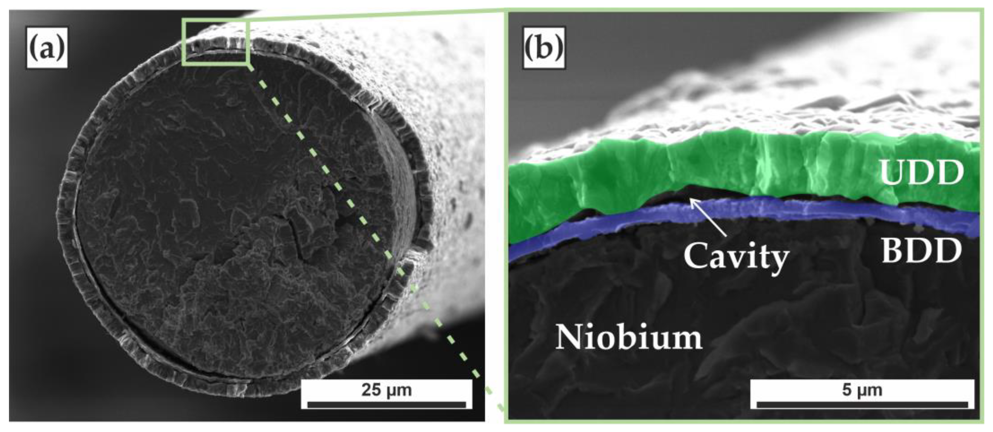
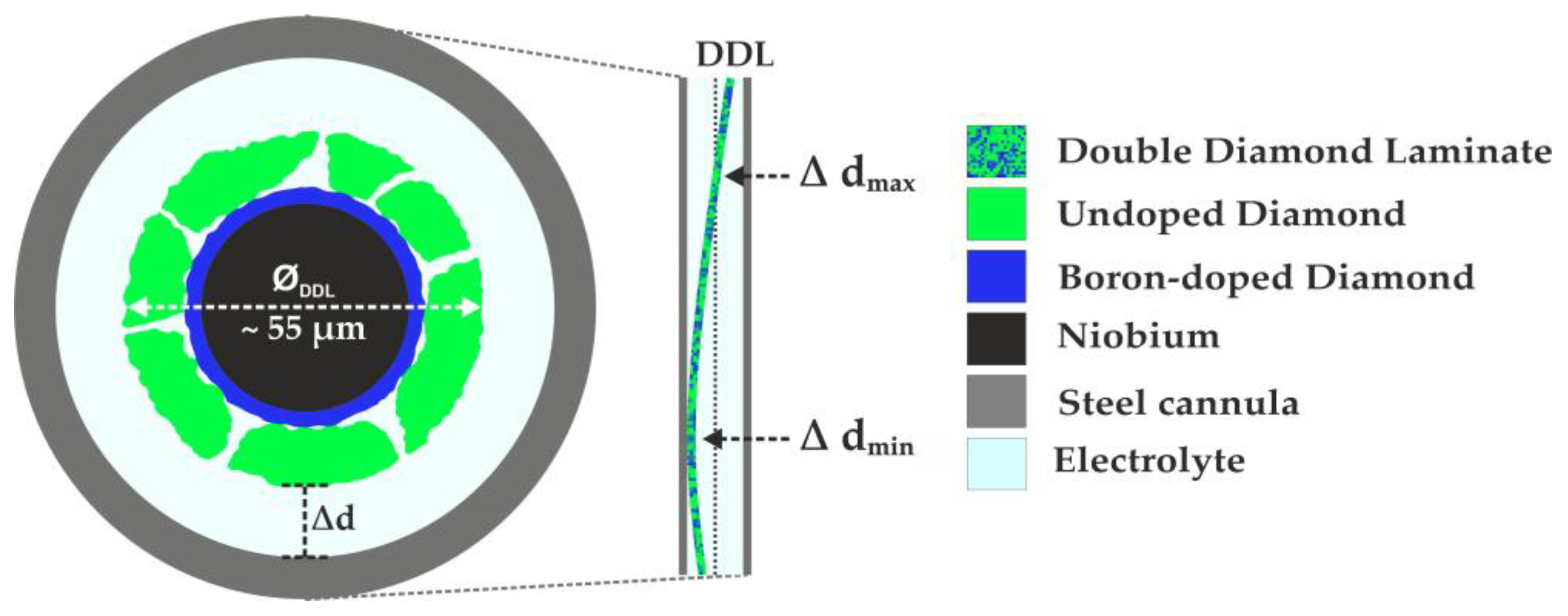
3.2. Double Diamond Laminate
3.3. Formation of Active BDD Sites as a Spotted Pattern
3.4. Oxidant Production Screening with DDL
4. Discussion
4.1. Diamond as Insulation and Electrochemical Active Site
4.2. Introduction of a More Realistic Model of DDL
4.3. Beneficial Properties of DDL Electrodes with Microdistancing
5. Conclusions and Outlook
6. Patents
Supplementary Materials
Author Contributions
Funding
Institutional Review Board Statement
Informed Consent Statement
Data Availability Statement
Acknowledgments
Conflicts of Interest
References
- Nidheesh, P.V.; Divyapriya, G.; Oturan, N.; Trellu, C.; Oturan, M.A. Environmental applications of boron-doped diamond electrodes: 1. Applications in water and wastewater treatment. ChemElectroChem 2019, 6, 2124. [Google Scholar] [CrossRef]
- Ochiai, T.; Iizuka, Y.; Nakata, K.; Murakami, T.; Tryk, D.A.; Fujishima, A.; Koide, Y.; Morito, Y. Efficient electrochemical decomposition of perfluorocarboxylic acids by the use of a boron-doped diamond electrode. Diam. Relat. Mater. 2011, 20, 64–67. [Google Scholar] [CrossRef]
- Schorr, B.; Ghanem, H.; Rosiwal, S.; Geißdörfer, W.; Burkovski, A. Elimination of bacterial contaminations by treatment of water with boron-doped diamond electrodes. World J. Microbiol. Biotechnol. 2019, 35, 48. [Google Scholar] [CrossRef]
- Davis, J.; Baygents, J.C.; Farrell, J. Understanding persulfate production at boron doped diamond film anodes. Electrochim. Acta 2014, 150, 68–74. [Google Scholar] [CrossRef]
- Divyapriya, G.; Nidheesh, P.V. Electrochemically generated sulfate radicals by boron doped diamond and its environmental applications. Curr. Opin. Solid State Mater. Sci. 2021, 25, 100921. [Google Scholar] [CrossRef]
- Griesbach, U.; Malkowsky, I.M.; Waldvogel, S.R. Green electroorganic synthesis using BDD electrodes. In Electrochemistry for the Environment; Comninellis, C., Chen, G., Eds.; Springer: New York, NY, USA, 2010; pp. 125–141. [Google Scholar]
- Lips, S.; Waldvogel, S.R. Use of boron-doped diamond electrodes in electro-organic synthesis. ChemElectroChem 2019, 6, 1649–1660. [Google Scholar] [CrossRef]
- Waldvogel, S.R.; Mentizi, S.; Kirste, A. Boron-doped diamond electrodes for electroorganic chemistry. In Topics in Current Chemistry; Springer: Berlin/Heidelberg, Germany, 2012; Volume 320, pp. 1–32. [Google Scholar]
- Zhang, F.; Sun, Z.; Cui, J. Research on the mechanism and reaction conditions of electrochemical preparation of persulfate in a split-cell reactor using BDD anode. RSC Adv. 2020, 10, 33928–33936. [Google Scholar] [CrossRef]
- Tago, S.; Ochiai, T.; Suzuki, S.; Hayashi, M.; Kondo, T.; Fujishima, A. Flexible boron-doped diamond (BDD) electrodes for plant monitoring. Sensors 2017, 17, 1638. [Google Scholar] [CrossRef]
- Dwyer, D.J.; Kohanski, M.A.; Collins, J.J. Role of reactive oxygen species in antibiotic action and resistance. Curr. Opin. Microbiol. 2009, 12, 482–489. [Google Scholar] [CrossRef] [PubMed]
- Koch, M.; Rosiwal, S.; Burkovski, A. Environmentally sustainable elimination of microbes using boron-doped diamond electrodes. In Microbial Biotechnology; Chowdhary, P., Mani, S., Chaturvedi, P., Eds.; Wiley: Weinheim, Germany, 2022; pp. 355–364. [Google Scholar]
- Böhm, A.L.; Koch, M.; Rosiwal, S.; Burkovski, A.; Karl, M.; Grobecker-Karl, T. Electrochemical disinfection of experimentally infected teeth by boron-doped diamond electrode treatment. J. Clin. Med. 2019, 8, 2037. [Google Scholar] [CrossRef] [PubMed]
- Göltz, M.; Koch, M.; Detsch, R.; Karl, M.; Burkovski, A.; Rosiwal, S. Influence of in-situ electrochemical oxidation on implant surface and colonizing microorganisms evaluated by scanning electron microscopy. Materials 2019, 12, 3977. [Google Scholar] [CrossRef] [PubMed]
- Klär, V.; Palarie, V.; Burkovski, A.; Karl, M.; Grobecker-Karl, T. Pilot study on the applicability of boron-doped diamond electrodes for tooth whitening. Clin. Exp. Dent. Res. 2022, 8, 757–762. [Google Scholar] [CrossRef]
- Koch, M.; Palarie, V.; Göltz, M.; Kurzer, M.; Zulla, M.; Rosiwal, S.; Willner, M.; Burkovski, A.; Karl, M. Root canal obturation by electrochemical precipitation of calcium phosphates. Appl. Sci. 2022, 12, 2956. [Google Scholar] [CrossRef]
- Koch, M.; Palarie, V.; Koch, L.; Burkovski, A.; Zulla, M.; Rosiwal, S.; Karl, M. Preclinical testing of boron-doped diamond electrodes for root canal disinfection: A series of preliminary studies. Microorganisms 2022, 10, 782. [Google Scholar] [CrossRef]
- Koch, M.; Göltz, M.; Xiangjun, M.; Karl, M.; Rosiwal, S.; Burkovski, A. Electrochemical disinfection of dental implants experimentally contaminated with microorganisms as a model for periimplantitis. J. Clin. Med. 2020, 9, 475. [Google Scholar] [CrossRef] [PubMed]
- Koch, M.; Burkovski, A.; Zulla, M.; Rosiwal, S.; Geißdörfer, W.; Dittmar, R.; Grobecker-Karl, T. Pilot study on the use of a laser-structured double diamond electrode (DDE) for biofilm removal from dental implant surfaces. J. Clin. Med. 2020, 9, 3036. [Google Scholar] [CrossRef] [PubMed]
- Ochiai, T.; Ishii, Y.; Tago, S.; Hara, M.; Sato, T.; Hirota, K.; Nakata, K.; Murakami, T.; Einaga, Y.; Fujishima, A. Application of boron-doped diamond microelectrodes for dental treatment with pinpoint ozone-water production. ChemPhysChem 2013, 14, 2094–2096. [Google Scholar] [CrossRef]
- May, P.W.; Rego, C.A.; Thomas, R.M.; Ashfold, M.N.R.; Rosser, K.N.; Everitt, N.M. CVD diamond wires and tubes. Diam. Relat. Mater. 1994, 3, 810–813. [Google Scholar] [CrossRef]
- Manfredotti, C.; Fizzotti, F.; Lo Giudice, A.; Mucera, G.; Polesello, P.; Vittone, E.; Mankelevich, Y.A.; Suetin, N.V. Growth and characterisation of CVD diamond wires for X-ray detection. Diam. Relat. Mater. 1997, 6, 1051–1056. [Google Scholar] [CrossRef]
- Abada, H.M.; Hashem, A.A.R.; Abu-Seida, A.M.; Nagy, M.M. The effect of changing apical foramen diameter on regenerative potential of mature teeth with necrotic pulp and apical periodontitis. Clin. Oral. Investig. 2022, 26, 1843–1853. [Google Scholar] [CrossRef] [PubMed]
- Asai, K.; Einaga, Y. Fabrication of an all-diamond microelectrode using a chromium mask. Chem. Commun. 2019, 55, 897–900. [Google Scholar] [CrossRef]
- Holt, K.B. Diamond ultramicroelectrodes and nanostructured electrodes. In Synthetic Diamond Films: Preparation, Electrochemistry, Characterization and Applications; Brillas, E., Martinez-Huitle, C.A., Eds.; John Wiley: Hoboken, NJ, USA, 2011; p. 133. [Google Scholar]
- Pagels, M.; Hall, C.E.; Lawrence, N.S.; Meredith, A.; Jones, T.G.J.; Godfried, H.P.; Pickles, C.S.J.; Wilman, J.; Banks, C.E.; Compton, R.G.; et al. All-diamond microelectrode array device. Anal. Chem. 2005, 77, 3705–3708. [Google Scholar] [CrossRef]
- Einaga, Y. Boron-doped diamond electrodes: Fundamentals for electrochemical applications. Acc. Chem. Res. 2022, 55, 3605–3615. [Google Scholar] [CrossRef]
- McBeath, S.T.; Wilkinson, D.P.; Graham, N.J.D. Application of boron-doped diamond electrodes for the anodic oxidation of pesticide micropollutants in a water treatment process: A critical review. Environ. Sci. Water Res. Technol. 2019, 5, 2090–2107. [Google Scholar] [CrossRef]
- Borchardt, R.; Sand, P.; Fromm, T.; Rosiwal, S. Novel structuring technique for diamond coatings. Diam. Relat. Mater. 2020, 110, 108103. [Google Scholar] [CrossRef]
- Didier, C.M.; Kundu, A.; Deroo, D.; Rajaraman, S. Development of in vitro 2D and 3D microelectrode arrays and their role in advancing biomedical research. J. Micromech. Microeng. 2020, 30, 103001. [Google Scholar] [CrossRef]
- Martínez-Huitle, C.A.; Brillas, E. A critical review over the electrochemical disinfection of bacteria in synthetic and real wastewaters using a boron-doped diamond anode. Curr. Opin. Solid State Mater. Sci. 2021, 25, 100926. [Google Scholar] [CrossRef]
- Long, Y.; Ni, J.; Wang, Z. Subcellular mechanism of Escherichia coli inactivation during electrochemical disinfection with boron-doped diamond anode: A comparative study of three electrolytes. Water Res. 2015, 84, 198–206. [Google Scholar] [CrossRef]
- Jeong, J.; Kim, J.Y.; Yoon, J. The role of reactive oxygen species in the electrochemical inactivation of microorganisms. Environ. Sci. Technol. 2006, 40, 6117–6122. [Google Scholar] [CrossRef]


Disclaimer/Publisher’s Note: The statements, opinions and data contained in all publications are solely those of the individual author(s) and contributor(s) and not of MDPI and/or the editor(s). MDPI and/or the editor(s) disclaim responsibility for any injury to people or property resulting from any ideas, methods, instructions or products referred to in the content. |
© 2023 by the authors. Licensee MDPI, Basel, Switzerland. This article is an open access article distributed under the terms and conditions of the Creative Commons Attribution (CC BY) license (https://creativecommons.org/licenses/by/4.0/).
Share and Cite
Zulla, M.; Vierheilig, V.; Koch, M.; Burkovski, A.; Karl, M.; Rosiwal, S. Diamond as Insulation for Conductive Diamond—A Spotted Pattern Design for Miniaturized Disinfection Devices. C 2023, 9, 78. https://0-doi-org.brum.beds.ac.uk/10.3390/c9030078
Zulla M, Vierheilig V, Koch M, Burkovski A, Karl M, Rosiwal S. Diamond as Insulation for Conductive Diamond—A Spotted Pattern Design for Miniaturized Disinfection Devices. C. 2023; 9(3):78. https://0-doi-org.brum.beds.ac.uk/10.3390/c9030078
Chicago/Turabian StyleZulla, Manuel, Vera Vierheilig, Maximilian Koch, Andreas Burkovski, Matthias Karl, and Stefan Rosiwal. 2023. "Diamond as Insulation for Conductive Diamond—A Spotted Pattern Design for Miniaturized Disinfection Devices" C 9, no. 3: 78. https://0-doi-org.brum.beds.ac.uk/10.3390/c9030078