Review

Nonvolatile Voltage Controlled Molecular Spin-State Switching for Memory Applications

1
Department of Physics and Astronomy, University of Nebraska-Lincoln, Lincoln, NE 68588, USA
2
Advanced Light Source, Lawrence Berkeley National Laboratory, Berkeley, CA 94720, USA
3
Physics Department, Indiana University Purdue University-Indianapolis, Indianapolis, IN 46202, USA
4
Physics Department, Oklahoma State University, Stillwater, OK 74078, USA
5
Advanced Materials Sciences, Sandia National Laboratories, Albuquerque, NM 87185, USA
6
Molecular Foundry, Lawrence Berkeley National Laboratory, Berkeley, CA 94720, USA
7
Department of Electrical Engineering, University of Texas at Dallas, Richardson, TX 75080, USA
8
School of Electrical and Computer Engineering, Georgia Institute of Technology, 791 Atlantic Drive N.W., Atlanta, GA 30332, USA
*
Authors to whom correspondence should be addressed.
Contributed equally to this work.
Submission received: 26 January 2021 / Revised: 18 February 2021 / Accepted: 8 March 2021 / Published: 11 March 2021
(This article belongs to the Special Issue Spin Crossover Materials: Towards Applications in Devices)

Abstract

:
Nonvolatile, molecular multiferroic devices have now been demonstrated, but it is worth giving some consideration to the issue of whether such devices could be a competitive alternative for solid-state nonvolatile memory. For the Fe (II) spin crossover complex [Fe{H2B(pz)2}2(bipy)], where pz = tris(pyrazol-1-yl)-borohydride and bipy = 2,2′-bipyridine, voltage-controlled isothermal changes in the electronic structure and spin state have been demonstrated and are accompanied by changes in conductance. Higher conductance is seen with [Fe{H2B(pz)2}2(bipy)] in the high spin state, while lower conductance occurs for the low spin state. Plausibly, there is the potential here for low-cost molecular solid-state memory because the essential molecular thin films are easily fabricated. However, successful device fabrication does not mean a device that has a practical value. Here, we discuss the progress and challenges yet facing the fabrication of molecular multiferroic devices, which could be considered competitive to silicon.

1. Introduction

As the expectations for novel organic electronics grow, the design of flexible and high-density nonvolatile memory device remains a hot topic. The successes with organic electronics, combined with indications of success in addressing the complex grand challenge of manipulating magnetically ordered states by electrical means, suggest new approaches and applications to develop novel spintronics. In molecular systems, the spin crossover (SCO) relates to the transition between a low spin (LS) of the metal ion (indeed, diamagnetic state in the case of the Fe2+ system) to a high-spin (HS) paramagnetic state in 3D transition metal compounds, and for quite some time now, it has been suggested that the spin crossover (SCO) phenomenon has potential applicability in molecular spintronic devices [1,2,3,4,5,6,7,8,9,10,11,12,13,14,15]. In such device elements, based on the molecular spin state, is very likely that state switching may be accomplished without large current densities or power consumption. Molecular systems have the very real possibility of providing a room temperature device on a length scale less than 10 nm while delivering low-power nonvolatile local magneto-electric memory operations.
We have investigated heteromolecular devices from molecular ferroelectrics and spin crossover molecular complex [Fe{H2B(pz)2}2(bipy)], where pz = tris(pyrazol-1-yl)-borohydride and bipy = 2,2′-bipyridine [13,14]. Such devices work where the voltage control of the molecular spin states leads to nonvolatile conductance changes [13,14]. From these many perspectives of memory devices [1,2,3,4,5,6,7,8,9,10,11,12,13,14] made possible by the molecular spin-state transition, we can construct a list of some of the key elements needed to make a competitive nonvolatile molecular device for memory applications.
Spin crossover molecular systems have a long history [16,17,18,19,20,21], but as successful nonvolatile devices that can be manipulated by voltage alone, the success is much more recent [12,13,14]. Nonetheless, a picture has emerged [5,7,8,12,22,23] of some of the key criteria needed to make a molecular spintronic device, based on spin crossover complexes, competitive with silicon technology. These identified criteria are as follows:
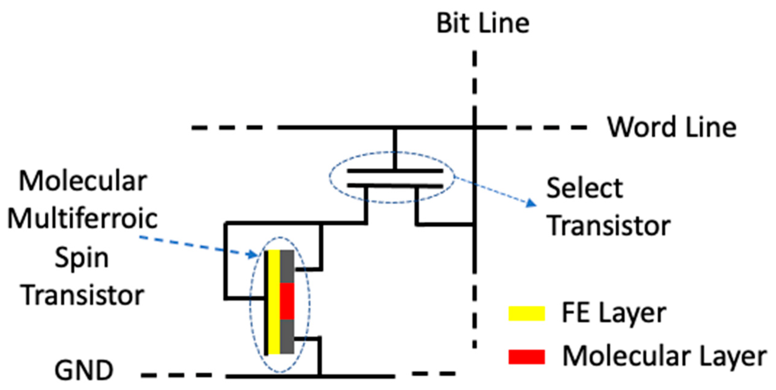
  • A device implementation scheme;
  • The ability to make a thin film;
  • The ability to “lock” the spin state (i.e., nonvolatility);
  • The ability to isothermally “unlock” and switch the spin state, ideally with voltage;
  • A low coercive voltage (ideally less than 1 V) and low write peak currents (ideally 104 A/cm2);
  • A conductance change with spin state;
  • Room-temperature operation and at temperatures well above room temperature;
  • A device on/off ratio > 10;
  • An on-state device resistivity less than 1 Ω·cm;
  • A device fast switching speed, ideally less than 100 ps;
  • Device reproducibility;
  • Device endurance, ideally 1016 switches without degradation;
  • The ability of having a nonvolatile device with a transistor channel width of 40 nm or below.
Nonvolatile devices that are both two-terminal diode-like devices [13] and effectively four-terminal transistor devices [13,14] have been fabricated from spin crossover molecules. Both are seen to operate at room temperature. The diode or two-terminal multiferroic molecular devices are very much like the nonvolatile tunnel junction devices, in terms of implementation, for which there is considerable literature [24,25,26,27] and indeed a commercial product [28,29,30,31]. The two-terminal spin crossover heteromolecular nonvolatile device [13] could be very competitive, because the on/off ratio of the oxide tunnel barrier magnetic tunnel junction is typically very low, often less than 2 [32,33,34,35].
Existing memory components are configured in numerous ways, the most common being SRAM (static random-access memory), DRAM (dynamic random-access memory), and NAND flash. They each have their own distinct advantages in memory cell area and read or write time. Spin-state molecular devices have inherent memory, so they do not benefit from being configured as an SRAM memory cell, where a positive feedback loop provides the memory storage rather than being provided by the device itself. In a similar way, memory, based on the nonvolatile manipulation of molecular spin state, is likely not suitable for configuration in a “NAND Flash” memory arrays, due to read difficulties and write difficulties associated with the very high resistance of these molecular devices, as noted below. However, the basic DRAM cell consists of an access transistor and a capacitive storage element. We can use the same concept of an access transistor but substitute the capacitor with a spin-state molecular device. Figure 1 shows a schematic of a plausible nonvolatile memory element cell. This memory cell is based on the field effect voltage-controlled spin state molecular transistor described elsewhere [12,13,14] and could exploit the difference between the low-resistance and high-resistance states of a voltage-controlled spin-state molecular memory device fabricated from spin crossover complexes. However, unlike DRAM (dynamic random-access memory), where charge storage on the cell must be refreshed periodically, molecular spin-state memory is nonvolatile, as noted above and elsewhere [12,13,14], and the output is resistive. This is particularly useful when low-power memory is needed. The select transistor may be any appropriate transistor switch. It could be a silicon NMOS (n-channel MOSFET) device, a tunnel field-effect transistor (TFET), or even another molecular multiferroic spin transistor, providing that switching does not allow for any memory storage in the select transistor.
With this DRAM-like configuration, read is achieved by activating the required bit line to a voltage high enough that the resistance of the multiferroic transistor may be read but low enough that programming cannot occur. Then, the word line is activated, so the resistance of a particular multiferroic transistor may be read. Read is achieved with a current sensing amplifier, as the read voltage is typically in the tens to hundreds of millivolts, and a current sense amplifier is more robust in these conditions. It is anticipated that the sense amplifier will be constructed in conventional MOS technology. In order to write a state into the spin transistor, the bit line is raised to the positive reprogramming voltage to program a “1” state or lowered to a sufficiently negative voltage that the transistor is programmed to the “0” state.
As indicated elsewhere in this article, this particular variant of a nonvolatile memory element would not be the only implementation scheme for a potential nonvolatile spin crossover molecular device, but it provides a context for reviewing the experimentally demonstrated properties of spin crossover molecular devices and spin crossover complexes in the context of what would be needed for a competitive nonvolatile molecular device. Other types of memory architecture are possible utilizing this room temperature voltage-controlled spin state molecular memory device technology.
Here, we seek to outline the key characteristics of the successful room-temperature nonvolatile spin crossover devices in the context of what must be achieved and demonstrated for such devices to be competitive against silicon technology. This is not only a roadmap for future work but also a basis for benchmarking the molecular spintronics devices against silicon technology and other beyond CMOS device concepts.

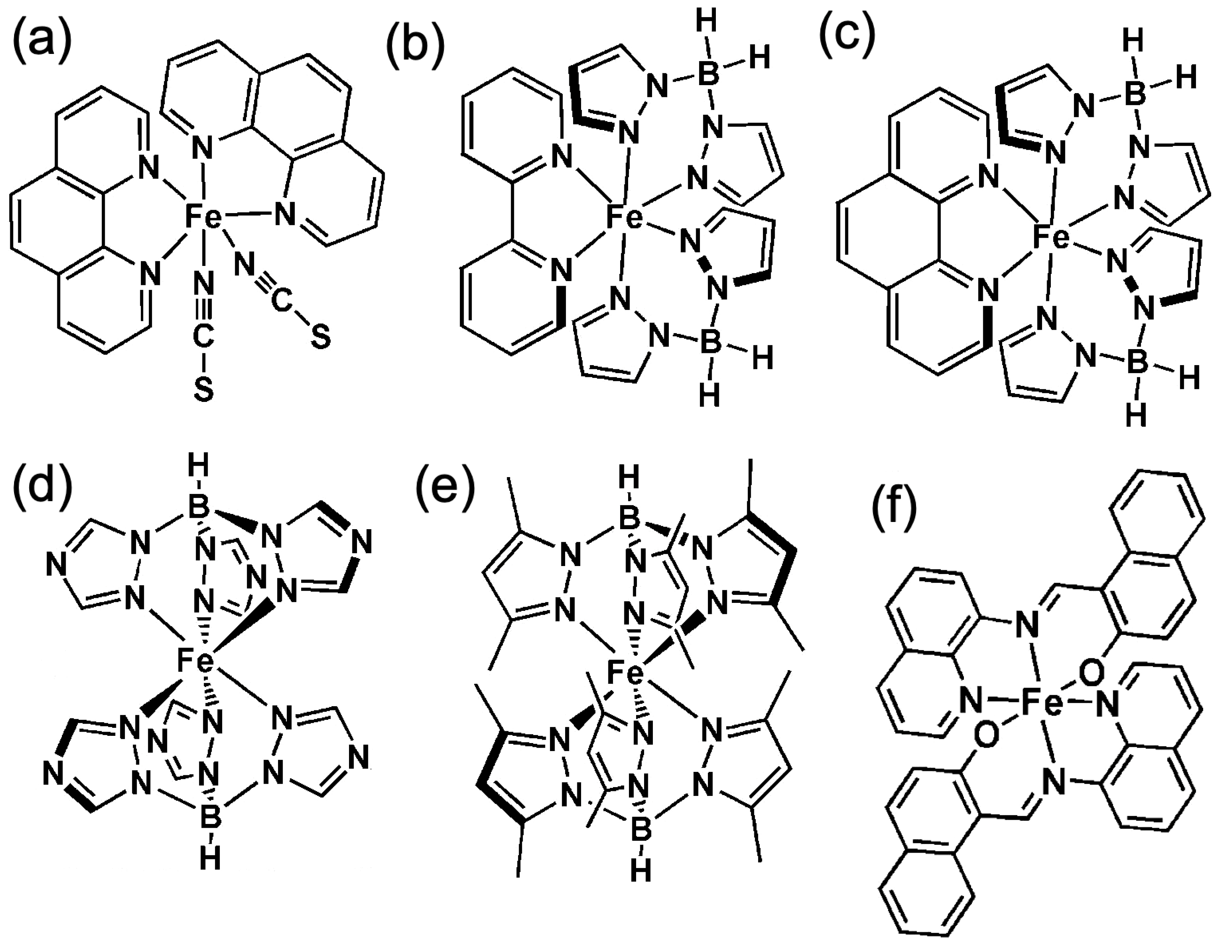
2. Making a Spin Crossover Molecular Thin Film

A competitive device requires scalability. This is to say that there has to be a route to large scale manufacturability. This tends to negate single molecule devices [12] for the simple reason that there are insurmountable barriers to the fabrication of such devices into a 1 GB memory array. Large device arrays require thin films. There are three approaches. These are to build a spin crossover thin film architecture chemically, as has been done in the case of [Fe-(pz){Pd(CN4)}] [36,37], evaporate a thin film, or spin coat a thin film from solution.
The more widely used approach to film fabrication is to evaporate a thin film of spin crossover molecules [8]. This will not work with all spin crossover molecular systems, because the sublimation process must leave the molecules “intact”, and the condensation process must result in a suitable molecular packing on the local scale (at least), so that the properties that change across the spin transition can be exploited reproducibly. The requirements tend to exclude molecular salts and polymers, as neither can be evaporated readily. Yet the approach has been successfully applied to [Fe(1,10-phenanthroline)2(NCS)2] (frequently known as Fe(phen)2(NCS)2) [38,39,40,41,42,43,44], as illustrated in Figure 2a, [Fe(H2B(pz)2)2phen] where H2B(pz)2 = dihydrobis(1H-pyrazol-1-yl)borate [45,46,47,48,49,50,51], as illustrated in Figure 2c, [Fe(HB(tz)3)2] (tz = 1,2,4-triazol-1-yl) [52,53,54,55,56], as illustrated in Figure 2d, [Fe(HB(3,5-(CH3)2(pz)3)2], where pz = pyrazolyl [10,57,58,59,60,61], as illustrated in Figure 2e, [Fe(qnal)2] where qnal = quinoline-naphthaldehyde [62], as illustrated in Figure 2f, [Fe(HB(pz)3)2] where pz = pyrazolyl [11,63], and the molecule that is the focus of this review: [Fe{H2B(pz)2}2(bipy)] where (H2B(pz)2 = bis(hydrido)bis(1H-pyrazol-1-yl)borate, bipy = 2,2′-bipyridine) [13,14,64,65,66,67,68,69,70,71,72,73,74,75,76,77], as illustrated in Figure 2b.
Another approach would be to spin coat the molecular layers from solution, as in the case of Fe(hptrz)3](OTs)2 (hptrz = 4-heptyl-1,2,4-triazole, OTs = tosylate) [78]. The problem with making the thin film from solution is that solvent effects are known to alter the characteristics of the spin-state transition for some spin crossover complexes [79,80]. This is not likely to be an insurmountable problem, but realistically, the molecular solubility and solvent effects are issues that would have to be addressed if this were chosen as the route to large scale device fabrication. Presently, efforts to explore solubility and solvent effects are only in their infancy.

3. Locking the Molecular Spin State

A competitive nonvolatile device requires locking of the spin state in the region of room temperature, as has been achieved with the inclusion of both dipolar molecular additives [73,81] as well as from the influence of the substrate. Key here is that the polarization of a ferroelectric interface can preferentially favor the adoption of the high or low spin state of an adjacent spin cross molecular thin film [13,14,72,77] over a wide range of temperatures from 100 K [72] to 350 K [14]. It is important to note that this influence of the ferroelectric substrate domain polarization extends away from the interface with ferroelectric and well into the adjacent spin crossover molecular thin film. The exact mechanisms for this influence of the substrate on the spin state of the molecular spin crossover complex thin film have not been precisely identified, but intermolecular cooperative effects are implicated in the influence of the substrate on the adjacent spin crossover molecular thin film [71]. The fact that the interface polarization influences the spin-state occupancy significantly for molecular spin crossover complex thin films up to 20 molecular layers [71], and for even greater film thicknesses in a somewhat diminished manner [14] means that device fabrication does not require precise and stringent film thickness choices, easing the constraints.
Thus far, there is no evidence of finite scaling effects that would lead to diminished critical temperatures with thinner films, although intermolecular cooperativity is seen to vary with film thickness [71]. The result is that isothermal switching (as discussed below) is more complete, and spin-state locking is more effective in thinner films than thicker films. We note, in passing, that the surface of molecular spin crossover complex thin film may have a different spin-state occupancy than the rest of the film [71]. Furthermore, since the device has to be both top and bottom gated, the molecular spin crossover complex thin film will be influenced by two different interfaces, and the effects of the latter have not yet been investigated in detail.

4. Isothermal Molecular Spin-State Switching

A competitive nonvolatile molecular spin crossover device requires change of the spin state, ideally with voltage, from one nonvolatile state to another. This is the device “write” operation and has now been demonstrated [13,14]. Recent studies [74,82] suggest that an applied magnetic field could reduce the activation barrier to a change in spin state, but as with light activation of a spin state change [69,77], this does not seem to lend itself toward a readily applicable memory application. Just the same, isothermal spin state and conductance switching has been demonstrated. It is this achievement of nonvolatile voltage control of the molecular spin state [13,14] that opens the door to potential practical applications. The adjacent ferroelectric layer provides a low coercivity voltage control of the spin state, as well as nonvolatility, but the device practicalities favor the use of organic [13,14] rather than inorganic [77] ferroelectrics, as discussed next.
Isothermal switching of the spin state optically, in the vicinity of room temperature, is certainly well established [55,57,58,73,74,83,84,85,86,87,88,89], as there are a number of photoactive spin crossover molecules, and optically switching has been a route to probing spin-state switching speed (as discussed below). However, these other routes to isothermal switching of the spin state (pressure changes, light, etc.) are not a route to a competitive memory device.

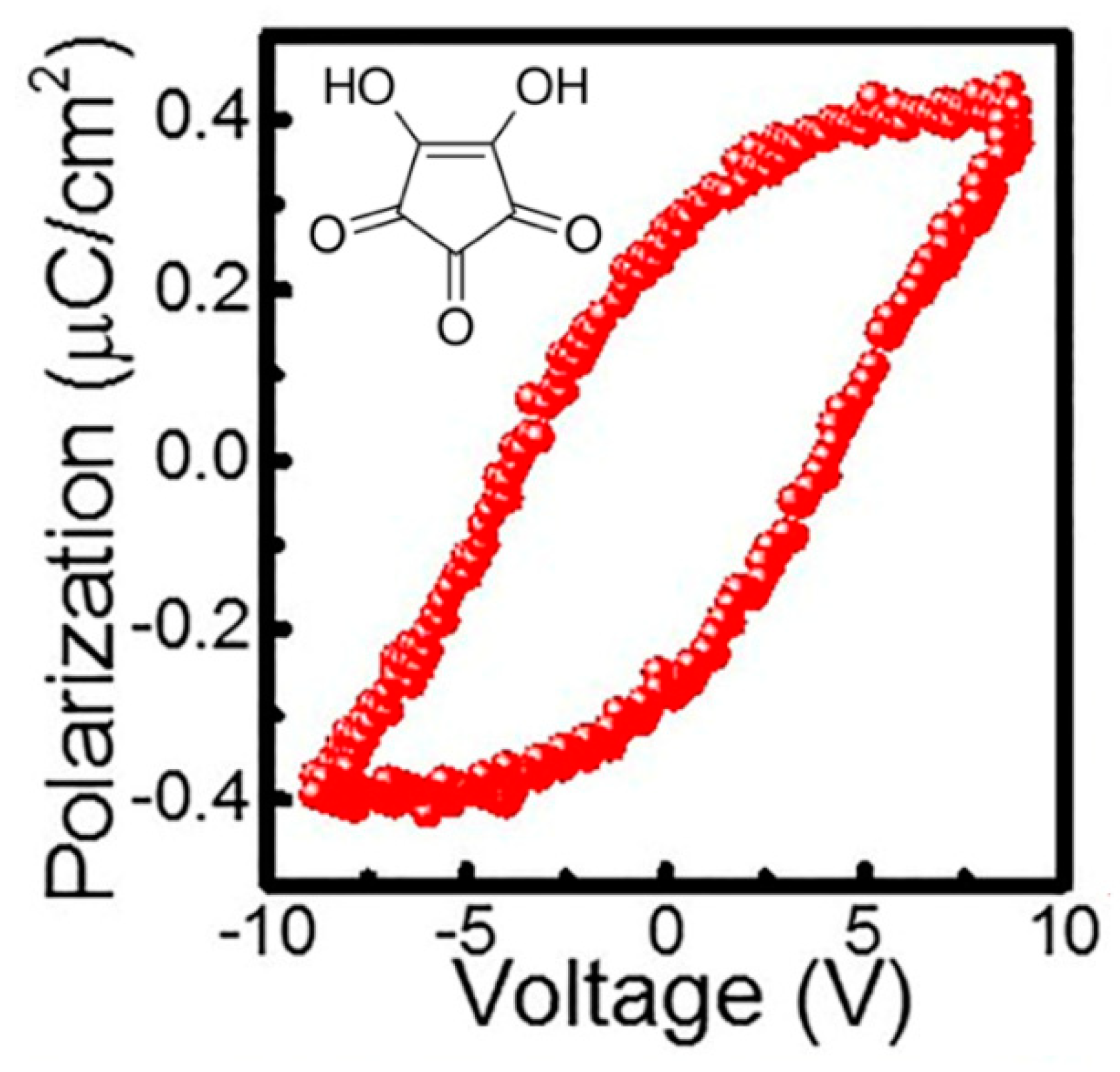
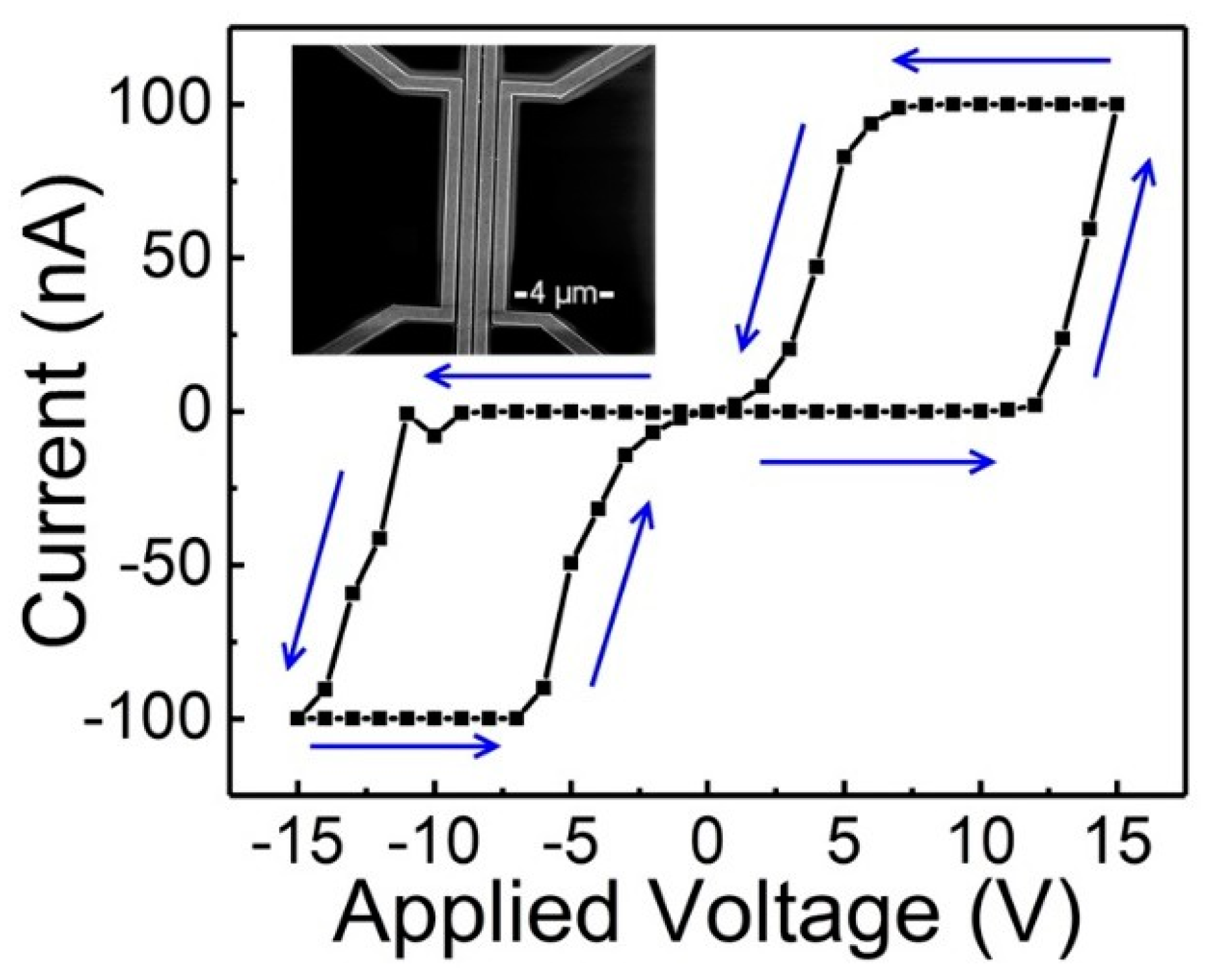
5. The Search for a Low Coercive Voltage and Low Peak Write Currents

The working nonvolatile molecular spin crossover devices fabricated so far [12,13,14] make use of a ferroelectric layer adjacent to the spin crossover molecular layer. Thus, the coercive voltage of the device tends to be dominated by the coercive voltage of the ferroelectric layer. Obviously, the choice of molecular ferroelectric also plays a role. Coercive voltages of 1.5 V have been obtained for a five-layer poly(vinylidene fluoride with trifluoroethylene) film [90], and roughly 5 V has been obtained for both 35 nm and 185 nm thick croconic acid thin films [91], respectively (Figure 3). The good news here is that the coercive voltage for the ferroelectric layer tends to scale with the ferroelectric layer film thickness, but sadly, this scaling with film thickness appears to be far from perfect [92,93,94,95] in the thin film limit. Yet a critical electric field Ecr of roughly 50 MVm−1 [95] and 0.2–0.4 GVm−1 [94,96,97] have been estimated for poly(vinylidene fluoride with trifluoroethylene) films, meaning that coercive voltages of 50 mV to 0.2 V are possible for bilayer thick molecular films of about 1 nm thickness. Even with failures of scaling in the thin film limit, coercive voltages of less than 0.5 V should be possible for bilayer thick molecular films [90]. The critical electric field Ecr of less than 2 MVm−1 [97,98] for croconic acid means that coercive voltages less than 3 mV might be possible, which in fact would be too small to be practical, so thicker and thus more reliable ferroelectric thin films would be required.
While there have been some successes with inorganic ferroelectric layers influencing the spin state of an adjacent molecular spin crossover complex thin film [77], in general, the problems with the inorganic ferroelectric layers are that, apart from PbZr0.2Ti0.8O3 (PZT), the coercive voltages tend to be somewhat higher, outside of the tunnel junction geometry where the coercive voltages also are in the range of 1 V [99,100]. In the very thinnest of oxide ferroelectric films, ferroelectric polarization retention tends to be lower [100]. Indeed, our experience is that in the very thin oxide ferroelectric films, one ferroelectric polarization is favored so that the retention of one ferroelectric polarization is favored over another. Thin film oxide ferroelectrics, even when grown on oxide surfaces, tend to exhibit preferential upward polarization (C+) [101,102]. This is not desirable in a nonvolatile device destined for memory applications. For the oxides, surface defects abound. How a spin crossover complex will bond at such defects sites is not yet clear, so concerns remain that spin-state switching will be suppressed for spin crossover complexes residing at such oxide surface imperfections.
Organic ferroelectric thin films are also far from perfect in their behavior. First, there is the problem that the faster the switching speed, the higher the coercive voltage needed [87]. Second, the coercive voltages for each ferroelectric polarization direction may differ as the film thickness decreases [79]. The loss of symmetry in the coercive voltage can be the result of the interface with a conducting contact [92]. Organic ferroelectric thin films also tend to exhibit preferential upward polarization [103]. Finally, there is the problem that the polarization hysteresis is not “square”, meaning that the application of higher voltage, the coercive voltage, may be necessary to achieve full polarization.
If the current density is 1 electron per molecule in 1 ns, this translates into an overall minimum current density of 3.6 × 10⁵ A/cm2. This approaches the industry goal of a current density of 104 A/cm2. This is because the gate supply needs to be able to do two things: (1) be able to make the device switch the polarization of the ferroelectric gate dielectric, and hence the spin state in the spin crossover molecular layer (where the latter plays the role of the semiconductor channel in the transistor geometry) at a reasonable supply voltage. In other words, the gate supply voltage should not be too high and not too low. If the gate supply voltage required is too high, then the implementation of room temperature nonvolatile spin crossover transistor molecular devices would require high-voltage supplies or charge pumps on chip in order to program a memory device. This is why EEPROM is not a very popular nonvolatile memory device—it simply requires too much supply voltage to make it a very usable memory. If the gate supply voltages are too significant, this would limit the application of nonvolatile spin crossover transistor molecular devices to one-time-programmable memory only. On the other hand, if the programming voltage could be brought down to a very low value, it has the advantage of making the memory chip easy to program, but circuitry then has to be carefully designed to ensure that accidental programming does not occur especially during the read operations. (2) The second factor to be considered is speed of write. While less important than the ability to write a memory cell, speed is nonetheless important, and it becomes more important in memory applications requiring a fast write time. Unfortunately, the writing or programing voltage and the write speed requirements can act against each other in operational memory, since the lower the programming or write voltage, the better it is for the write time, but reducing the programming voltage too much increases the chances of a write “disturb” event.
We do know that the molecular ferroelectric gate dielectrics can be made as thin as 1 nm and still be reliable [90,96], and the coercive voltage would be <0.5 V. A gate dielectric 2 nm thick would be “worry free” with a coercive voltage of about 0.8 V or less. A ferroelectric gate dielectric any thicker than that would result in an unnecessary increase in the coercive voltage and an increase in the current needed to “write” the gate ferroelectric correctly. The desire for faster write speeds means that the peak current densities needed to provide the correct ferroelectric polarization at the gate will also scale up. There has to be recognition that there is a trade-off between faster write speeds and lower peak current densities for a “write” operation.

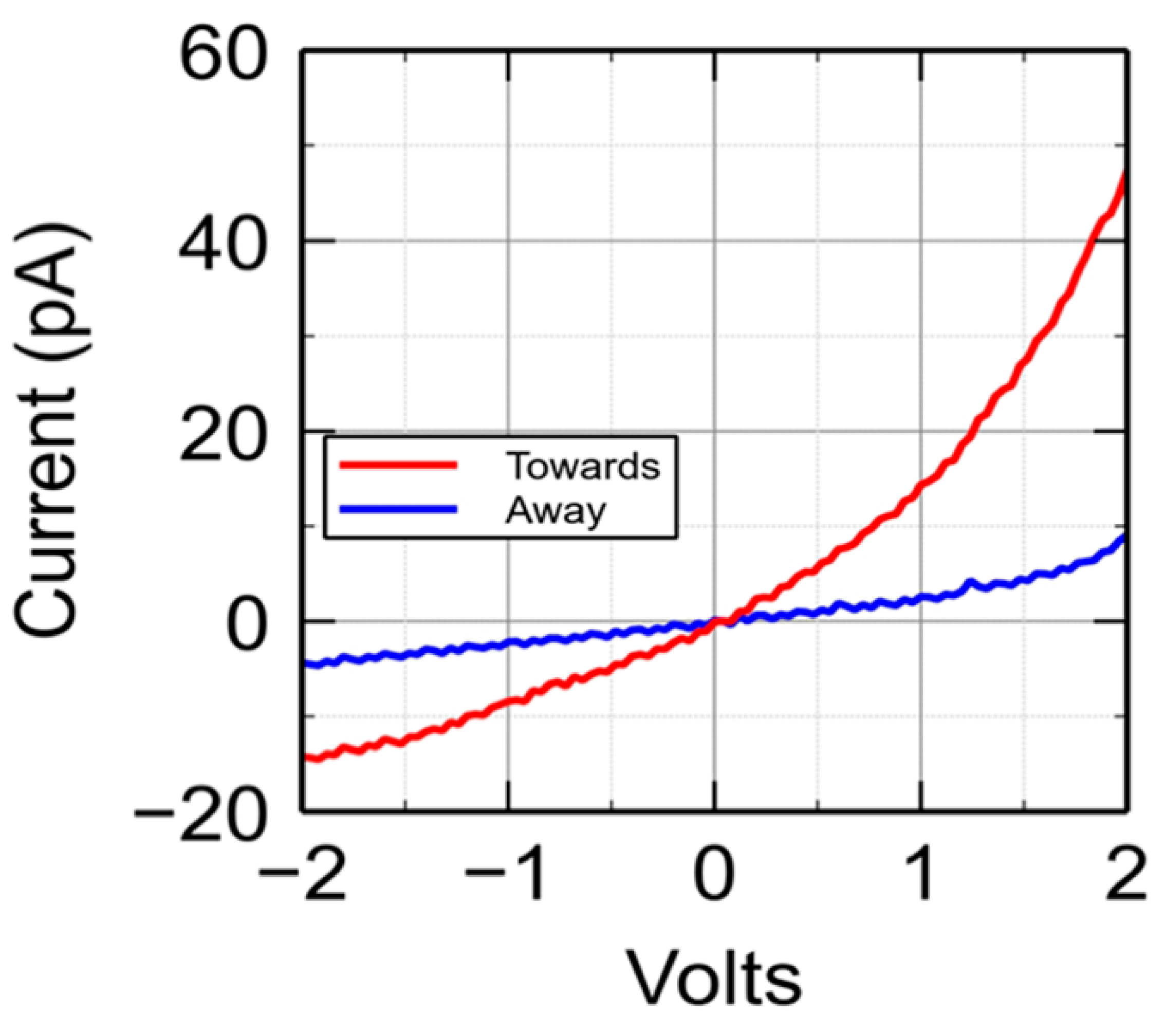
6. Isothermal Switching of Conductance in a Nonvolatile Spin Crossover Molecular Device

Along with the device write operation, a nonvolatile molecular device requires a read operation. So far, the read operation has been successfully exploiting the conductance change that accompanies the change in molecular spin state [12,13,14], as seen in Figure 4. In part, this conductance change may be associated with the known changes to the highest occupied molecular orbital to lowest unoccupied molecular orbital gap that occur with a change in spin state. For [Fe{H2B(pz)2}2(bipy)], the highest occupied molecular orbital to lowest unoccupied molecular orbital gap is much larger (by about 2 eV [72]) in the low spin state than the high spin state. A smaller band gap for the high spin state of [Fe{H2B(pz)2}2(bipy)] is consistent with a higher conductance, and this higher conductance is seen in working room temperature devices [13,14]. This type of conductance change has been observed with other spin crossover complexes, such as [Fe(bpz)2phen] [51], Fe(trans- bis(3-(2-pyridyl)(1,2,3)triazolo(1–5)pyridine)bis(isothiocyanato)] [104], Rb0.8Mn[Fe(CN)6]0.93·1.62H2O [105], [Fe(trz)3](BF4)2 (trz = triazole) [22], [Fe(phen)2(NCS)2] [38], and [FeIII(qsal)2][Ni(dmit)2]3·CH3CN·H2O [106], although in these latter examples, the conductance change was volatile.

7. Room-Temperature Operation of a Nonvolatile Spin Crossover Molecular Device

Device stability and reliability, at room temperature, is now a given. There are now working nonvolatile molecular devices fabricated from spin crossover complexes that work not only at room temperature [12,13,14] but to temperatures well above room temperature [14]. Working nonvolatile molecular device operation has been demonstrated at temperatures as high as 350 K [14]. While higher temperatures have not yet been tested in the working device, higher operational device temperatures are indicated. The spin crossover molecules that can be evaporated as thin films typically sublime between 433 and 510 K [8], which suggests molecular stability at these temperatures. Of course, molecular stability at high temperatures is not the only consideration, as too high a temperature may lead to material loss through sublimation, even if it does not lead to molecular degradation. Overall, given the current status, it does seem that nonvolatile molecular devices fabricated from spin crossover complexes are operational over a wide enough temperature range to be both practical and competitive.

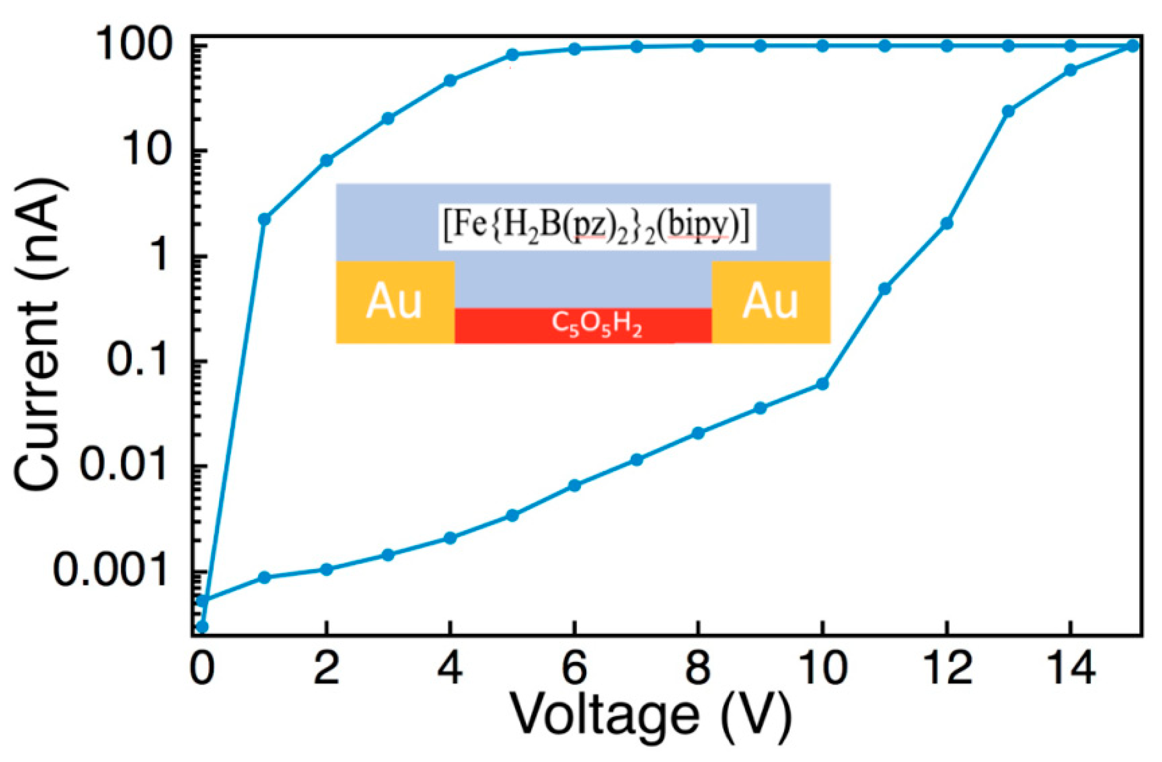
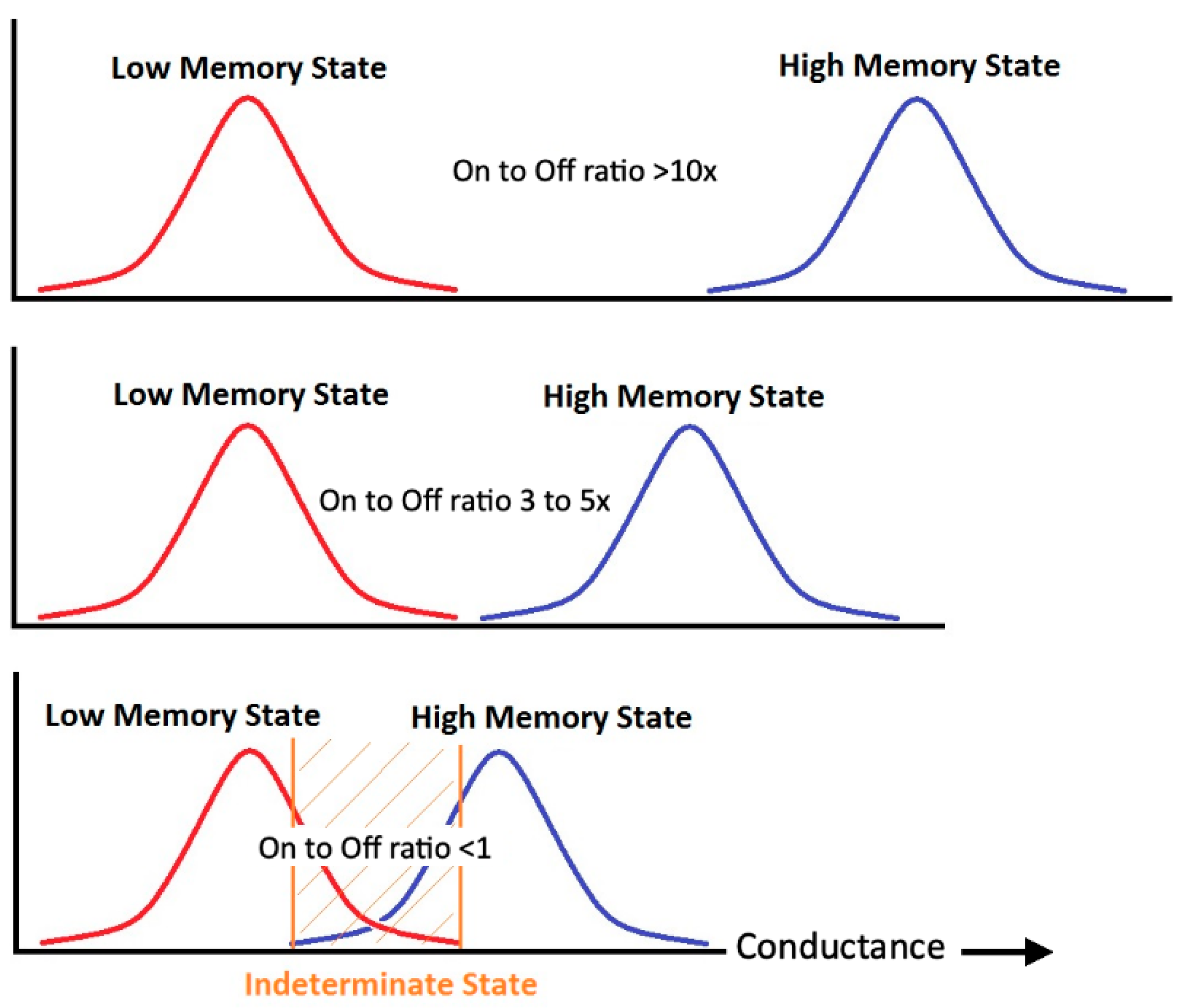
8. Improving the Molecular Nonvolatile Multiferroic Device On/Off Ratio

Nonvolatile molecular devices, based on a change of molecular spin state, should exhibit a high level of fidelity in possible molecular electronics applications. The initial working nonvolatile molecular devices, based on the spin crossover complex [Fe{H2B(pz)2}2(bipy)], had an on/off ratio of about 4 to 5 [13,14], for the devices in the transistor geometry. With more complete spin-state switching, there are indications that the on/off ratio can be increased greater than 100 [14].
While a homogeneous ferroelectric layer is very desirable for nonvolatile molecular multiferroics devices in the transistor geometry because the ferroelectric is a gate dielectric layer for one of the gates (either top or bottom), more complete spin-state switching occurs in the volatile conductance switching that arises in a two-terminal device when the ferroelectric layer is more homogeneous. The data from such a two-terminal diode-like device, as opposed to the top and bottom gated transistor device, shows such a device to be volatile, as shown in Figure 5. Here, current on/off ratios of 104 have been obtained, with 103 near the threshold voltage, as indicated in Figure 6. This high on/off ratio, as seen in Figure 6, suggests that the changes in conductance, associated with a spin-state change, can be engineered to be very significant. Yet, nonvolatility is possible in the longitudinal conductance for a two-terminal diode device, as reported elsewhere [13].
The on/off current ratios are greater than 10 and frequently greater than 100 in many of the two-terminal volatile spin crossover molecular devices [54]. These higher (>10) on/off ratios are good for a memory cell and ease the pathway to implementation. This is because, in practice, memory cells are not typically uniform. There is a statistical range of cell resistances and device to device on/off ratios. As the on–off ratio decreases, there is a point where the on/off ratio is sufficient, so there is an overlap between the “high” state and the “low” state. When this occurs, there is the potential for error, which in some cases can be corrected but at the expense of error correction circuitry. Figure 7 illustrates the issue of state overlap if on/off ratio is reduced too much.
The device characteristics discussed after this, which are needed for competitive nonvolatile multiferroic molecular devices fabricated from spin crossover molecular complexes, have not been integrated into a working device. Integration of the additional possibly valuable characteristics described in the following sections represents the challenges for the future. When working with such small currents, as may be involved in switching a multiferroic device, other circuit effects, such as capacitance and resistance impact what can be readily measured directly.

9. Reducing the On-State Resistance of a Spin Crossover Molecular Device

From the geometry of the devices fabricated so far, particularly from the nonvolatile multiferroic molecular two terminal diode-like devices, we can estimate that the resistance in the on state is about 103 Ω·cm and 106 Ω·cm in the off state for a spin crossover device based on [Fe{H2B(pz)2}2(bipy)]. For a nanoscale device, this presents a serious problem, because if the resistance scales with size, the nanoscale device will have a total resistance that diminishes utility. This is evident from the schematic of the transistor in Figure 8.
Here, a resistance of 103 Ω·cm translates to a device resistance of 5 GΩ when the dimensions of the device are reduced to a 10 nm width, a source to drain distance of 10 nm, and a film thickness of 2 nm according to:
R = ρ L W T = 10 3 × 10 2 ( Ω · m ) × 10 × 10 9 m ( 10 × 10 9 m ) ( 2 × 10 9 m ) = 5   G Ω
This 5 GΩ resistance is simply too high a resistance to be valuable from an applications point of view, especially as this may not correctly include resistance at the molecule–metal contact interface, which is a known problem discussed further below. The large impedance will lead to delay times that are simply too long to be competitive. Just the same, it has to be realized that [Fe{H2B(pz)2}2(bipy)] is probably not the most desirable spin crossover complex for competitive nonvolatile molecular devices for memory applications. Other spin crossover molecular complexes are reported with lower on-state resistance of 5 Ω·cm for the spin crossover molecules [Fe(tpma)(xbim)](X)(TCNQ)1.5·DMF (X=ClO4) [107] and [FeIII(sal2-trien)][Ni(dmit)2] [108]. An even lower on-state resistance of 0.5 Ω·cm [95] has been reported for the spin crossover molecule [FeIII(qsal)2][Ni(dmit)2]3·CH3CN·H2O. This strongly suggests that the reduction of the intrinsic resistance of a spin crossover molecular system is a problem that can be addressed by some adroit synthetic chemistry.
Another approach is to use the spin crossover molecular thin film as part of the gate dielectric to a high-mobility graphene device and modulate the conductance in the graphene layer, as demonstrated recently [10,109,110]. This is not regarded here as a competitive approach because of the problems associated with graphene as the channel width shrinks to less than 50 nm [111,112,113,114,115], namely significant increases in effective carrier mass, large edge scattering, and low carrier mobilities, not to mention the problems associated with scaling to large arrays using graphene nanoribbons. On the other hand, spin crossover complexes combined with carbon nanotubes may provide a viable memory device alternative [116].
While the devices made so far have source-to-drain on-state resistances of 103 Ohm·cm, there are options from ongoing chemistry [106,107,108] where the on-state resistance could be as low as 0.5 Ohm·cm. These other spin crossover molecules have not been fabricated into a working nonvolatile molecular transistor, but if applicable from a fabrication point of view, for a transistor at the 10 nm node with the channel at 0.5 Ohm·cm resistance, this would lead to a source-to-drain resistance of 2.5 MΩ in a spin crossover transistor device 10 nm wide and 2 nm thick.

10. Faster Device Switching Speeds for a Nonvolatile Spin Crossover Molecular Device

There are spin crossover complexes that may have spin-state switching speeds adequate for a competitive device. A number of measurements suggest sub-picosecond switching speeds [55,117]. This means that the switching speed is limited by the switching speed of the ferroelectric. For copolymers of polyvinylidene fluoride (PVDF), this means that the reversal of a ferroelectric domain will take far longer than a nanosecond, because of the need to rotate the -CH2CF2- chemical formulae units. Benzimidazole, 2-methylbenzimidazole [108], 5,6-dichloro-2-methylbenzimidazole [118], bridged bis(benzimidazole) [119], and croconic acid [91,98] are molecular ferroelectrics that require far less dramatic atomic repositioning and thus potentially should have faster ferroelectric polarization switching speeds.
Device switching speed is not simply determined by the switching speed of the molecular state and configuration. Resistance, as discussed above, can play a big role in determining the overall operational speed of the device. This latter point is complicated not just by the resistance of the spin crossover molecular layer, which acts to reduce the operation speed of the device but a variety of parasitic capacitances. The demonstration that the magnetic field reduces the activation barrier separating the high and low spin states [82] does suggest that faster switching speed may be possible with the application of a magnetic field, but this may be an unwanted complication in the implementation of nonvolatile multiferroic molecular devices fabricated from spin crossover molecular complexes for memory.
It should also be noted that as the device on/off ratio decreases, it takes longer to isolate the correct state (on or off) when doing a read function. Read time is typically more important than write time, since typically, there are more read than write cycles, especially in nonvolatile memory configurations. A moderately high on/off ratio of more than 103, as suggested by the current changes seen for more complete spin-state switching for data taken in in the transistor geometry [14], may be possible. This higher on/off ratio would allow for faster sense amplifiers and a variety of memory configurations. This suggests that there is promise for these types of devices and the existing devices are more than adequate for memory applications from the perspective of the on/off ratio.
Understudied but a huge concern is the contact potential. Organic layers are known to have a molecular band offset when interfaced with a metal [120,121,122]. This is typically about 200 meV, but it can vary widely. We simply do not know if there is sufficiently reliable and efficient carrier injection into nonvolatile molecular devices fabricated from spin crossover complexes. So far, this issue of contact potentials and molecular band offsets has not been investigated, but it could have a profound effect on the overall device speed.

11. Reproducibility for Nonvolatile Spin Crossover Molecular Devices

At this point, not much is known about device reproducibility simply because very few devices have been made, and the emphasis has been on the fabrication of different nonvolatile spin crossover molecular devices to demonstrate the fact that such devices work at all. Yet, this is a question that demands attention. Any large variation in either on-state or off-state conductance from one nonvolatile molecular device fabricated from spin crossover complexes to the next device would limit the wide-scale applicability or require greater on/off ratios. Unless the process of large-scale nonvolatile multiferroic molecular devices fabricated from spin crossover molecular complexes can be made both sufficiently reliable and uniform, then wide scale applicability is a chimera.

12. Nonvolatile Spin Crossover Molecular Device Endurance, Without Degradation

Although molecular devices are generally considered very fragile compared to inorganic devices, endurance may not be the issue once feared. Recently, there have been molecular spin crossover devices fabricated that have been shown to undergo 10 million switches without degradation [56]. These demonstration spin crossover molecular devices were not designed for nonvolatile voltage-controlled memory applications; just the same, this recent demonstration of spin-state switching endurance [56] provides considerable evidence in favor of spin crossover molecular devices. The limits of possible endurance without degradation have not been tested in spite of the fact that these are molecular devices.

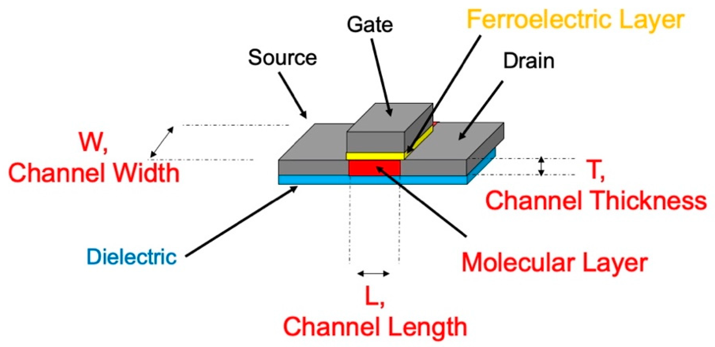
13. The Potential for Transistor Widths on the Tens of Nanometer Scale or Less

With almost all devices dependent on magneto-electric coupling, there is the concern that there is a limit to the device size. In other words, there is concern that the magneto-electric coupling either suffers from some sort of finite scaling or that there is a critical volume where magneto-electric coupling simply fails. In the case of spin crossover systems, spin-state switching at room temperature has been demonstrated to the 3.6 ± 0.8 nm scale [123]. Again, this demonstration [123] provides considerable evidence that devices at the 10 nm scale are possible, and this would be competitive with silicon (CMOS) technologies. Yet the on-state resistance is high, as discussed above. Even a decrease of the on-state resistance to about 0.5 Ω·cm through a better choice of spin crossover complex would still mean a substantial device resistance on the nanometer scale. While the materials properties indicate that spin-state switching is possible below 10 nm, the exigencies of device implementation may preclude this implementation of nonvolatile voltage-controlled spin crossover molecular devices at dimensions below 10 nm as a result of the high on-state resistance as discussed above. Yet, depending on the lithography resolution, the source–drain distance could be decreased to lower the device resistance.
If the spin crossover molecular film thickness, acting as the semiconductor channel, is increased to 15 nm (experimentally shown to work [14,72]), this drops the device source to drain resistance to 667 MΩ. If a spin crossover complex with an on-state resistance of 0.5 Ω·cm is utilized, then the resistance drops further to 333 KΩ. For a transistor at the 20 nm node, this decreases the device source-to-drain resistance further to 167 KΩ. At the 30 nm node, device source-to-drain resistance drops even further to 111 KΩ, and at a channel width to 50 nm node, the resistance would about 67 KΩ.

14. Conclusions

While working room-temperature nonvolatile spin crossover molecular devices have been fabricated by placing a spin crossover molecular thin film adjacent to a molecular ferroelectric layer [12,13,14], a competitive device has not been demonstrated. Yet, there has been considerable progress in meeting the challenges that need to be satisfied. Of the dozen actual device issues listed in the introduction, seven of the challenges have been met and addressed in a working device.
A competitive nonvolatile multiferroic molecular device, fabricated from spin crossover molecular complexes, still needs to be demonstrated. The challenges that must be addressed but have not yet been realized in a working device, are clearly a smaller on-state resistance, faster switching speeds, low coercive voltages, and low peak power write current densities in reproducible working devices at the 10 to 50 nm scale that can endure 1016 switches, as indicated in Table 1.
A crude estimate of the write energy can be made, as even if the device is a perfect capacitor between the top and bottom gates with perfect gate dielectric layers, to reverse the electric field, current has to flow. If we assume perfect charge ionization, then the maximum current required to switch the ferroelectric polarization is determined by the required charge of one electron per dipole. Assuming one electron per molecule [96] and a molecular bilayer of ferroelectric, with a coercive voltage of 0.2, the write energy for a nonvolatile multiferroic transistor, fabricated from spin crossover molecular complexes, would be in the region of 70 aJ, which is far less than the roughly 100 fJ write energy of STT RAM at 65 nm [32,124] and comparable to the 15 pJ write energy expected of ferroelectric RAM at 45 to 65 nm [125]. This estimate for nonvolatile multiferroic devices fabricated from spin crossover molecular complexes neglects the device contact resistance, which is likely to be significant because of the molecular band offsets [120,121,122], as noted above. Given the exigencies associated with device implementation, a more realistic write energy for the nonvolatile multiferroic molecular device would be in the region of 0.7 fJ (about 10 times the estimated floor) or higher.
The question is whether nonvolatile multiferroic devices fabricated from spin crossover molecular complexes with transistor widths of 30, 40, or 50 nm are competitive. With an on-state resistance estimated to be about 67 KΩ per device at a transistor width of 50 nm and a spin crossover complex on state resistance of 0.5 Ωcm, these devices begin to appear to have practical value. There are certainly circumstances where devices with a resistance of 100 KΩ can be used for memory [126]. With the DRAM-type device arrangement, the gate is connected to the drain, so it may be that the best resistance goal would be something around 200 KΩ. The prospect of getting close to this goal seems to be increasingly realistic.
The speed of the memory read is the major factor of concern when we consider device resistance. There is no hard limit to resistance maximum, but for every doubling of memory resistance, to a first-order approximation, the read time doubles. For some types of memory, for example NAND flash, a very slow read time is acceptable, but this is in order to achieve a very compact memory cell. In the case of magneto-electric memory cells, the base cell size is bigger than the flash cell, and so this arena of very compact memory is not an area where nonvolatile multiferroic molecular devices fabricated from spin crossover molecular complexes is likely to be competitive. Instead, the target for nonvolatile multiferroic molecular devices fabricated from spin crossover molecular complexes is faster cache memories. With these possible implementations, it is acceptable to increase the width of the memory cell, within limits, and a cell width up to about 80 nm (with gate length of 12 nm) may be acceptable. A major advantage of the nonvolatile multiferroic devices fabricated from spin crossover molecular complexes is that there is the possibility of 3D integration of this technology, which can drastically increase the memory capacity. The fact that the multiferroic molecular device fabrication temperatures are low allows many layers of such devices to be fabricated on a silicon chip without damaging the underlying silicon transistor devices. This becomes particularly interesting in the case of crossbar arrays of nonvolatile multiferroic molecular devices, as in that implementation, one does not need one silicon transistor per each cell.
The nonvolatile multiferroic devices fabricated from spin crossover molecular complexes also appear to be competitive with zinc–tin oxide thin-film transistors [127] and other amorphous oxide semiconductor transistor schemes that might be used in flexible electronics such as displays [128]. After all, the nonvolatile multiferroic devices fabricated from spin crossover molecular complexes are molecular thin film devices and thus flexible.

Author Contributions

Conceptualization, A.J.Y., A.M. (Aaron Mosey), R.C., A.T.N., X.X. and P.A.D.; methodology, A.M. (Aaron Mosey), X.J., K.R.S. and G.T.W.; validation, G.H., A.S.D., X.J., A.J.Y., T.K.E., X.X. and R.C.; formal analysis, G.H., A.M. (Andrew Marshall), A.T.N., R.C. and P.A.D.; investigation, G.H., A.M. (Aaron Mosey), A.T.N. and A.M. (Andrew Marshall); resources, J.Z. and A.T.N.; writing—original draft preparation, G.H. and P.A.D.; writing—review and editing, A.M. (Andrew Marshall), A.N., X.X. and R.C.; supervision, A.T.N., R.C., X.X. and P.A.D.; project administration, A.T.N., R.C. and P.A.D.; funding acquisition, R.C. and P.A.D. All authors have read and agreed to the published version of the manuscript.

Funding

This research was supported by the National Science Foundation through NSF-DMR 2003057 (G.H., A. Mosey, A.D., T.K.E., R.C., P.A.D.), the Nebraska MRSEC (DMR-1420645) (X.J., P.X.Z., J.Z., X.X.) and through Grant No. NSF-ECCS 1740136 (A.J.Y., A.N.). Also funded through the nCORE, a wholly owned subsidiary of the Semiconductor Research Corporation (SRC), through the Center on Antiferromagnetic Magneto-electric Memory and Logic Task ID 2760.002 and Task ID 2760.003 (A.N., A.J.Y.). Use of the Advanced Light Source, Lawrence Berkeley National Laboratory, was supported by the U.S. Department of Energy (DOE) under contract no. DE-AC02-05CH11231. The lithography was funded in part by Sandia’s LDRD Program and was performed, in part, at the Center for Integrated Nanotechnologies, a U.S. DOE Basic Energy Sciences user facility. Sandia National Laboratories is a multi-mission laboratory managed and operated by National Technology & Engineering Solutions of Sandia, LLC, a wholly owned subsidiary of Honeywell International Inc., for the U.S. Department of Energy’s National Nuclear Security Administration under contract DE-NA0003525. This paper describes objective technical results and analysis. Any subjective views or opinions that might be expressed in the paper do not necessarily represent the views of the U.S. Department of Energy or the United States Government.

Data Availability Statement

The data presented in this study arises from the sources cited or are available on request from the corresponding authors.

Acknowledgments

The authors would like to thank Dmitri Nikonov, Gabor Molnár and Azzedine Bousseksou for extremely helpful discussions.

Conflicts of Interest

The authors declare no conflict of interest. The funders had no role in the design of the study; in the collection, analyses, or interpretation of data; in the writing of the manuscript, or in the decision to publish the results.

References

  1. Kahn, O.; Martinez, C.J. Spin-Transition Polymers: From Molecular Materials toward Memory Devices. Science 1998, 279, 44–48. [Google Scholar] [CrossRef]
  2. Bousseksou, A.; Molnár, G.; Salmon, L.; Nicolazzi, W. Molecular Spin Crossover Phenomenon: Recent Achievements and Prospects. Chem. Soc. Rev. 2011, 40, 3313–3335. [Google Scholar] [CrossRef]
  3. Bousseksou, A.; Molnár, G.; Demont, P.; Menegotto, J. Observation of a Thermal Hysteresis Loop in the Dielectric Constant of Spin Crossover Complexes: Towards Molecular Memory Devices. J. Mater. Chem. 2003, 13, 2069–2071. [Google Scholar] [CrossRef]
  4. Kumar, K.S.; Ruben, M. Emerging Trends in Spin Crossover (SCO) Based Functional Materials and Devices. Coord. Chem. Rev. 2017, 346, 176–205. [Google Scholar] [CrossRef]
  5. Molnár, G.; Rat, S.; Salmon, L.; Nicolazzi, W.; Bousseksou, A. Spin Crossover Nanomaterials: From Fundamental Concepts to Devices. Adv. Mater. 2018, 30, 17003862. [Google Scholar] [CrossRef]
  6. Rotaru, A.; Dugay, J.; Tan, R.P.; Guralskiy, I.A.; Salmon, L.; Demont, P.; Carrey, J.; Molnár, G.; Respaud, M.; Bousseksou, A. Nano-electromanipulation of Spin Crossover Nanorods: Towards Switchable Nanoelectronic Devices. Adv. Mater. 2013, 25, 1745–1749. [Google Scholar] [CrossRef] [PubMed] [Green Version]
  7. Lefter, C.; Davesne, V.; Salmon, L.; Molnár, G.; Demont, P.; Rotaru, A.; Bousseksou, A. Charge Transport and Electrical Properties of Spin Crossover Materials: Towards Nanoelectronic and Spintronic Devices. Magnetochemistry 2016, 2, 18. [Google Scholar] [CrossRef] [Green Version]
  8. Kumar, K.S.; Ruben, M. Sublimable Spin-crossover Complexes: From Spin-State Switching to Molecular Devices. Angew. Chem. Int. Ed. 2020, 59, 2–22. [Google Scholar] [CrossRef] [PubMed] [Green Version]
  9. Lefter, C.; Tan, R.; Dugay, J.; Tricard, S.; Molnár, G.; Salmon, L.; Carrey, J.; Nicolazzi, W.; Rotaru, A.; Bousseksou, A. Unidirectional Electric Field-Induced Spin-State Switching in Spin Crossover Based Microelectronic Devices. Chem. Phys. Lett. 2016, 644, 138–141. [Google Scholar] [CrossRef]
  10. Konstantinov, N.; Tauzin, A.; Noumbe, U.N.; Dragoe, D.; Kundys, B.; Majjad, H.; Brosseau, A.; Lenertz, M.; Singh, A.; Berciaud, S.; et al. Electrical read-out of light-induced spin transition in thin film spin crossover/graphene heterostructures. J. Mater. Chem. C 2021, 9, 2712–2720. [Google Scholar] [CrossRef]
  11. Mahfoud, T.; Molnár, G.; Cobo, S.; Salmon, L.; Thibault, C.; Vieu, C.; Demont, P.; Bousseksou, A. Electrical Properties and Non-Volatile Memory Effect of the [Fe(HB(pz)3)2] Spin Crossover Complex Integrated in a Microelectrode Device. Appl. Phys. Lett. 2011, 99, 053307. [Google Scholar] [CrossRef] [Green Version]
  12. Hao, G.; Cheng, R.; Dowben, P.A. The Emergence of the Local Moment Molecular Spin Transistor. J. Phys. Condens. Matter 2020, 32, 234002. [Google Scholar] [CrossRef]
  13. Hao, G.; Mosey, A.; Jiang, X.; Yost, A.J.; Sapkota, K.R.; Wang, G.T.; Zhang, X.; Zhang, J.; N’Diaye, A.T.; Cheng, R.; et al. Nonvolatile Voltage Controlled Molecular Spin State Switching. Appl. Phys. Lett. 2019, 114, 032901. [Google Scholar] [CrossRef] [Green Version]
  14. Mosey, A.; Dale, A.S.; Hao, G.; N’Diaye, A.T.; Dowben, P.A.; Cheng, R. Quantitative Study of Energy Change in Voltage-controlled Spin Crossover Molecules for Molecular Spintronics. J. Phys. Chem. Lett. 2020, 11, 8231–8237. [Google Scholar] [CrossRef]
  15. Khusniyarov, M.M. How to Switch Spin-Crossover Metal Complexes at Constant Room Temperature. Chem. Eur. J. 2016, 22, 15178–15191. [Google Scholar] [CrossRef]
  16. Cambi, L.; Cagnasso, A. Iron dithiocarbamates and nitrosodithiocarbamates. Atti. R. Accad. Naz. Lincei 1931, 13, 809. [Google Scholar]
  17. Cambi, L.; Szegö, L. Über die magnetische Susceptibilität der komplexen Verbindungen. Ber. Deutsch. Chem. Ges. B 1931, 64, 2591–2598. [Google Scholar] [CrossRef]
  18. Cambi, L.; Szegö, L.; Cagnasso, A. The Magnetic Susceptibility of Complexes. IV. Atti. R. Accad. Naz. Lincei 1932, 15, 266. [Google Scholar]
  19. Cambi, L.; Szegö, L.; Cagnasso, A. The magnetic susceptibility of complexes. V. Iron dibutyldithio-carbamates. Atti. R. Accad. Naz. Lincei 1932, 15, 329–335. [Google Scholar]
  20. Cambi, L.; Szegö, L. Über die magnetische Susceptibilität der komplexen Verbindungen (II. Mitteil.). Ber. Deutsch. Chem. Ges. B 1933, 66, 656–661. [Google Scholar] [CrossRef]
  21. Cambi, L.; Malatesta, L. Magnetismus und polymorphie innerer komplexsalze: Eisensalze der dithiocarbamidsäuren. Ber. Deutsch. Chem. Ges. B 1937, 70, 2067–2078. [Google Scholar] [CrossRef]
  22. Prins, F.; Monrabal-Capilla, M.; Osorio, E.A.; Coronado, E.; van der Zant, H.S.J. Room-Temperature Electrical Addressing of a Bistable Spin-Crossover Molecular System. Adv. Mater. 2011, 23, 1545–1549. [Google Scholar] [CrossRef] [PubMed]
  23. Weber, B.; Dowben, P.A. Preface to the JPCM special issue on molecular magnetism. J. Phys. Condens. Matter 2020, 32, 440201. [Google Scholar] [CrossRef] [PubMed]
  24. Zhu, B.J. Magnetoresistive Random Access Memory: The Path to Competitiveness and Scalability. Proc. IEEE 2008, 96, 1786–1798. [Google Scholar] [CrossRef]
  25. Yu, S.; Chen, P.-Y. Emerging Memory Technologies. IEEE Solid State Circuits Mag. 2016, 8, 43–56. [Google Scholar] [CrossRef]
  26. Senni, S.; Torres, L.; Sassatelli, G.; Gamatie, A.; Mussard, B. Exploring MRAM Technologies for Energy Efficient Systems-on-Chip. IEEE J. Emerg. Sel. Top. Circuits Syst. 2016, 6, 279–292. [Google Scholar] [CrossRef] [Green Version]
  27. Liao, Y.-C.; Pan, C.; Naeemi, A. Benchmarking and Optimization of Spintronic Memory Arrays. IEEE J. Explor. Solid-State Computat. Devices Circuits 2020, 6, 9–17. [Google Scholar] [CrossRef]
  28. Everspin 256Mb STT-MRAM (ST-DDR3). Available online: https://www.everspin.com/family/emd3d256m?npath=3557 (accessed on 15 November 2020).
  29. Everspin 1Gb STT-MRAM (ST-DDR4). Available online: https://www.everspin.com/family/emd4e001g?npath=3557 (accessed on 15 November 2020).
  30. Avalanche Technology Discrete MRAM, 50MHz Clock Rate in 1Mb and 4Mb Density Chips. Available online: https://www.avalanche-technology.com/products/discrete-mram/ (accessed on 15 November 2020).
  31. Kitagawa, E.; Fujita, S. TT-MRAM Cuts Power Use by 80%. In Proceedings of the 2013 IEEE International Electron Devices Meeting (IEDM 2013), Washington, DC, USA, 9–11 December 2013; Available online: http://www.eetimes.com/document.asp?doc_id=1280753 (accessed on 15 November 2020).
  32. Wang, K.L.; Alzate, J.G.; Amiri, P.K. Low-Power Non-Volatile Spintronic Memory: STT-RAM and Beyond. J. Phys. D Appl. Phys. 2013, 46, 074003. [Google Scholar] [CrossRef]
  33. Zhang, K.; Cao, K.; Zhang, Y.; Huang, Z.; Cai, W.; Wang, J.; Nan, J.; Wang, G.; Zheng, Z.; Chen, L.; et al. Rectified Tunnel Magnetoresistance Device With High On/Off Ratio for In-Memory Computing. IEEE Electron. Device Lett. 2020, 41, 928–931. [Google Scholar] [CrossRef]
  34. Patel, R.; Ipek, E.; Friedman, E.G. 2T–1R STT-MRAM memory cells for enhanced on/off current ratio. Microelectron. J. 2014, 45, 133–143. [Google Scholar] [CrossRef]
  35. Ohsawa, T.; Ikeda, S.; Hanyu, T.; Ohno, H.; Endoh, T. Trend of tunnel magnetoresistance and variation in threshold voltage for keeping data load robustness of metal–oxide–semiconductor/magnetic tunnel junction hybrid latches. J. Appl. Phys. 2014, 115, 17C728. [Google Scholar] [CrossRef]
  36. Cobo, S.; Molnár, G.; Real, J.A.; Bousseksou, A. Multilayer Sequential Assembly of Thin Films that Display Room Temperature Spin Crossover with Hysteresis. Angew. Chem. Int. Ed. 2006, 45, 5786–5789. [Google Scholar] [CrossRef]
  37. Molnár, G.; Cobo, S.; Real, J.A.; Carcenac, F.; Daran, E.; Vieu, C.; Bousseksou, A. A Combined Top-Down/Bottom-Up Approach for the Nanoscale Patterning of Spin-Crossover Coordination Polymers. Adv. Mater. 2007, 19, 2163–2167. [Google Scholar] [CrossRef]
  38. Miyamachi, T.; Gruber, M.; Davesne, V.; Bowen, M.; Boukari, S.; Scheurer, L.; Joly, F.; Rogez, G.; Yamada, T.K.; Ohresser, P.; et al. Robust Spin Crossover and Memristance Across a Single Molecule. Nat. Commun. 2012, 3, 938. [Google Scholar] [CrossRef]
  39. Briois, V.; Moulin, C.C.D.; Sainctavit, P.; Brouder, C.; Flank, A.-M. Full Multiple Scattering and Crystal Field Multiplet Calculations Performed on the Spin Transition FeII(phen)2(NCS)2 Complex at the Iron K and L2,3 X-ray Absorption Edges. J. Am. Chem. Soc. 1995, 117, 1019–1026. [Google Scholar] [CrossRef]
  40. Gruber, M.; Miyamachi, T.; Davesne, V.; Bowen, M.; Boukari, S.; Wulfhekel, W.; Alouani, M.; Beaurepaire, E. Spin crossover in Fe(phen)2(NCS)2 Complexes on Metallic Surfaces. J. Chem. Phys. 2017, 146, 092312. [Google Scholar] [CrossRef]
  41. Gruber, M.; Davesne, V.; Bowen, M.; Boukari, S.; Beaurepaire, E.; Wulfhekel, W.; Miyamachi, T. Spin State of Spin-Crossover Complexes: From Single Molecules to Ultrathin Films. Phys. Rev. B 2014, 89, 195415. [Google Scholar] [CrossRef]
  42. Ellingsworth, E.C.; Turner, B.; Szulczewski, G. Thermal Conversion of [Fe(phen)3](SCN)2 Thin Films into the Spin Crossover Complex Fe(phen)2(NCS)2. RSC Adv. 2013, 3, 3745–3754. [Google Scholar] [CrossRef]
  43. Beniwal, S.; Sarkar, S.; Baier, F.; Weber, B.; Dowben, P.A.; Enders, A. Site Selective Adsorption of the Spin Crossover Complex Fe(phen)2(NCS)2 on Au(111). J. Phys. Condens. Matter 2020, 32, 324003. [Google Scholar] [CrossRef]
  44. Shi, S.; Schmerber, G.; Arabski, J.; Beaufrand, J.-B.; Kim, D.J.; Boukari, S.; Bowen, M.; Kemp, N.T.; Viart, N.; Rogez, G.; et al. Study of molecular spin-crossover complex Fe(phen)2(NCS)2 thin films. Appl. Phys. Lett. 2009, 95, 043303. [Google Scholar] [CrossRef]
  45. Gopakumar, T.G.; Bernien, M.; Naggert, H.; Matino, F.; Hermanns, C.F.; Bannwarth, A.; Mühlenberend, S.; Krüger, A.; Krüger, D.; Nickel, F.; et al. Spin-Crossover Complex on Au(111): Structural and Electronic Differences Between Mono- and Multilayers. Chem. Eur. J. 2013, 19, 15702–15709. [Google Scholar] [CrossRef] [PubMed]
  46. Poggini, L.; Gonidec, M.; Balasubramanyam, R.K.; Squillantini, L.; Pecastaings, G.; Caneschi, A.; Rosa, P. Temperature-Induced Transport Changes in Molecular Junctions Based on a Spin Crossover Complex. J. Mater. Chem. C 2019, 7, 5343–5347. [Google Scholar] [CrossRef] [Green Version]
  47. Lefter, C.; Rat, S.; Sánchez Costa, J.; Manrique-Juárez, M.D.; Quintero, C.M.; Salmon, L.; Séguy, I.; Leichle, T.; Nicu, L.; Demont, P.; et al. Current Switching Coupled to Molecular Spin-States in Large-Area Junctions. Adv. Mater. 2016, 28, 7508–7514. [Google Scholar] [CrossRef] [PubMed] [Green Version]
  48. Ludwig, E.; Naggert, H.; Kalläne, M.; Rohlf, S.; Kröger, E.; Bannwarth, A.; Quer, A.; Rossnagel, K.; Kipp, L.; Tuczek, F. Iron(II) Spin-Crossover Complexes in Ultrathin Films: Electronic Structure and Spin-State Switching by Visible and Vacuum-UV Light. Angew. Chem. Int. Ed. 2014, 53, 3019–3023. [Google Scholar] [CrossRef] [PubMed] [Green Version]
  49. Schleicher, F.; Studniarek, M.; Kumar, K.S.; Urbain, E.; Katcko, K.; Chen, J.; Frauhammer, T.; Hervé, M.; Halisdemir, U.; Kandpal, L.M.; et al. Linking Electronic Transport through a Spin Crossover Thin Film to the Molecular Spin State Using X-ray Absorption Spectroscopy Operando Techniques. ACS Appl. Mater. Interfaces 2018, 10, 31580–31585. [Google Scholar] [CrossRef]
  50. Bernien, M.; Naggert, H.; Arruda, L.M.; Kipgen, L.; Nickel, F.; Miguel, J.; Hermanns, C.F.; Krüger, A.; Krüger, D.; Schierle, E.; et al. Highly Efficient Thermal and Light-Induced Spin-State Switching of an Fe(II) Complex in Direct Contact with a Solid Surface. ACS Nano 2015, 9, 8960–8966. [Google Scholar] [CrossRef] [PubMed]
  51. Gopakumar, T.G.; Matino, F.; Naggert, H.; Bannwarth, A.; Tuczek, F.; Berndt, R. Electron-Induced Spin Crossover of Single Molecules in a Bilayer on Gold. Angew. Chem. Int. Ed. 2012, 51, 6262–6266. [Google Scholar] [CrossRef]
  52. Poggini, L.; Gonidec, M.; González-Estefan, J.H.; Pecastaings, G.; Gobaut, B.; Rosa, P. Vertical Tunnel Junction Embedding a Spin Crossover Molecular Film. Adv. Electron. Mater. 2018, 4, 1800204. [Google Scholar] [CrossRef]
  53. Shalabaeva, V.; Ridier, K.; Rat, S.; Manrique-Juarez, M.D.; Salmon, L.; Séguy, I.; Rotaru, A.; Molnár, G.; Bousseksou, A. Room Temperature Current Modulation in Large Area Electronic Junctions of Spin Crossover Thin Films. Appl. Phys. Lett. 2018, 112, 013301. [Google Scholar] [CrossRef]
  54. Zhang, Y.; Séguy, I.; Ridier, K.; Shalabaeva, V.; Piedrahita-Bello, M.; Rotaru, A.; Salmon, L.; Molnár, G.; Bousseksou, A. Resistance Switching in Large-Area Vertical Junctions of the Molecular Spin Crossover Complex [Fe(HB(tz)3)2]: ON/OFF Ratios and Device Stability. J. Phys. Condens. Matter 2020, 32, 214010. [Google Scholar] [CrossRef] [PubMed]
  55. Ridier, K.; Bas, A.C.; Shalabaeva, V.; Nicolazzi, W.; Salmon, L.; Molnár, G.; Bousseksou, A.; Lorenc, M.; Bertoni, R.; Collet, E.; et al. Finite Size Effects on the Switching Dynamics of Spin-Crossover Thin Films Photoexcited by a Femtosecond Laser Pulse. Adv. Mater. 2019, 31, 1901361. [Google Scholar] [CrossRef] [PubMed]
  56. Ridier, K.; Bas, A.C.; Zhang, Y.; Routaboul, L.; Salmon, L.; Molnár, G.; Bergaud, C.; Bousseksou, A. Unprecedented Switching Endurance Affords for High-Resolution Surface Temperature Mapping Using a Spin-Crossover Film. Nat. Commun. 2020, 11, 3611. [Google Scholar] [CrossRef]
  57. Zhang, L.; Tong, Y.; Kelai, M.; Bellec, A.; Lagoute, J.; Chacon, C.; Girard, Y.; Rousset, S.; Boillot, M.-L.; Rivière, E.; et al. Anomalous Light-Induced Spin-State Switching for Iron(II) Spin-Crossover Molecules in Direct Contact with Metal Surfaces. Angew. Chem. Int. Ed. 2020, 59, 13341–13346. [Google Scholar] [CrossRef] [PubMed]
  58. Bairagi, K.; Iasco, O.; Bellec, A.; Kartsev, A.; Li, D.; Lagoute, J.; Chacon, C.; Girard, Y.; Rousset, S.; Miserque, F.; et al. Molecular-Scale Dynamics of Light-Induced Spin crossover in a Two-Dimensional layer. Nat. Commun. 2016, 7, 12212. [Google Scholar] [CrossRef]
  59. Bairagi, K.; Bellec, A.; Fourmental, C.; Iasco, O.; Lagoute, J.; Chacon, C.; Girard, Y.; Rousset, S.; Choueikani, F.; Otero, E.; et al. Temperature-, Light-, and Soft X-ray-Induced Spin Crossover in a Single Layer of FeII-Pyrazolylborate Molecules in Direct Contact with Gold. J. Phys. Chem. C 2018, 122, 727–731. [Google Scholar] [CrossRef]
  60. Iasco, O.; Boillot, M.-L.; Bellec, A.; Guillot, R.; Rivière, E.; Mazerat, S.; Nowak, S.; Morineau, D.; Brosseau, A.; Miserque, F.; et al. The Disentangling of Hysteretic Spin Transition, Polymorphism and Metastability in Bistable Thin Films Formed by Sublimation of Bis(scorpionate) Fe(II) Molecules. J. Mater. Chem. C 2017, 5, 11067–11075. [Google Scholar] [CrossRef]
  61. Fourmental, C.; Mondal, S.; Banerjee, R.; Bellec, A.; Garreau, Y.; Coati, A.; Chacon, C.; Girard, Y.; Lagoute, J.; Rousset, S.; et al. Importance of Epitaxial Strain at a Spin-Crossover Molecule−Metal Interface. J. Phys. Chem. Lett. 2019, 10, 4103–4109. [Google Scholar] [CrossRef] [PubMed]
  62. Atzori, M.; Poggini, L.; Squillantini, L.; Cortigiani, B.; Gonidec, M.; Bencok, P.; Sessoli, R.; Mannini, M. Thermal and Light-Induced Spin Transition in a Nanometric Film of a New High-Vacuum Processable Spin Crossover Complex. J. Mater. Chem. C 2018, 6, 8885–8889. [Google Scholar] [CrossRef]
  63. Zhao, T.; Dong, M.; Zhao, Y. A novel fabrication of [Fe(HB(pz)3)2]@MIL-101 hybrid material via diffusion and the lower temperature shift on its spin transition behavior. Appl. Phys. A 2019, 125, 670. [Google Scholar] [CrossRef]
  64. Warner, B.; Oberg, J.C.; Gill, T.G.; El Hallak, F.; Hirjibehedin, C.F.; Serri, M.; Heutz, S.; Arrio, M.A.; Sainctavit, P.; Mannini, M.; et al. Temperature- and Light-Induced Spin Crossover Observed by X-ray Spectroscopy on Isolated Fe(II) Complexes on Gold. J. Phys. Chem. Lett. 2013, 4, 1546–1552. [Google Scholar] [CrossRef] [Green Version]
  65. Pronschinske, A.; Bruce, R.C.; Lewis, G.; Chen, Y.; Calzolari, A.; Buongiorno-Nardelli, M.; Shultz, D.A.; You, W.; Dougherty, D.B. Iron(II) Spin Crossover Films on Au(111): Scanning Probe Microscopy and Photoelectron Spectroscopy. Chem. Commun. 2013, 49, 10446–10452. [Google Scholar] [CrossRef]
  66. Pronschinske, A.; Chen, Y.; Lewis, G.F.; Shultz, D.A.; Calzolari, A.; Buongiorno Nardelli, M.; Dougherty, D.B. Modification of Molecular Spin Crossover in Ultrathin Films. Nano Lett. 2013, 13, 1429. [Google Scholar] [CrossRef]
  67. Zhang, X.; Palamarciuc, T.; Rosa, P.; Létard, J.F.; Doudin, B.; Zhang, Z.; Wang, J.; Dowben, P.A. The Electronic Structure of a Spin Crossover Molecular Adsorbate. J. Phys. Chem. C 2012, 116, 23291–23296. [Google Scholar] [CrossRef]
  68. Beniwal, S.; Zhang, X.; Mu, S.; Naim, A.; Rosa, P.; Chastanet, G.; Létard, J.F.; Liu, J.; Sterbinsky, G.E.; Arena, D.A.; et al. Substrate-Induced Spin State Locking of the [Fe(H2B(pz)2)2(bipy)] Spin Crossover Complex. J. Phys. Condens. Matter 2016, 28, 206002. [Google Scholar] [CrossRef] [PubMed]
  69. Palamarciuc, T.; Oberg, J.C.; El Hallak, F.; Hirjibehedin, C.F.; Serri, M.; Heutz, S.; Letard, J.-F.; Patrick Rosa, P. Spin crossover materials evaporated under clean high vacuum and ultra-high vacuum conditions: From thin films to single molecules. J. Mater. Chem. 2012, 22, 9690. [Google Scholar] [CrossRef]
  70. Naggert, H.; Bannwarth, A.; Chemnitz, S.; von Hofe, T.; Quandt, E.; Tuczek, F. First Observation of Light-Induced Spin Change in Vacuum Deposited Thin Films of Iron Spin Crossover Complexes. Dalton Trans. 2011, 40, 6364–6366. [Google Scholar] [CrossRef]
  71. Jiang, X.; Hao, G.; Wang, X.; Mosey, A.; Zhang, X.; Yu, L.; Yost, A.J.; DiChiara, A.D.; Cheng, X.; Zhang, J.; et al. Tunable Spin-State Bistability in a Spin Crossover Molecular Complex. J. Phys. Condens. Matter 2019, 31, 315401. [Google Scholar] [CrossRef] [PubMed]
  72. Zhang, X.; Palamarciuc, T.; Létard, J.F.; Rosa, P.; Lozada, E.V.; Torres, F.; Rosa, L.G.; Doudin, B.; Dowben, P.A. Spin State of a Molecular Adsorbate Driven by the Ferroelectric Substrate Polarization. Chem. Commun. 2014, 50, 2255. [Google Scholar] [CrossRef] [Green Version]
  73. Zhang, X.; Costa, P.S.; Hooper, J.; Miller, D.P.; N’Diaye, A.T.; Beniwal, S.; Jiang, X.; Yin, Y.; Rosa, P.; Routaboul, L.; et al. Locking and Unlocking the Molecular Spin Cross-Over Transition. Adv. Mater. 2017, 29, 1702257. [Google Scholar] [CrossRef]
  74. Zhang, X.; Jiang, X.; Zhang, X.; Yin, Y.; Chen, X.; Hong, X.; Xu, X.; Dowben, P.A. Indications of Magnetic Coupling Effects in Spin Cross-over Molecular Thin Films. Chem. Commun. 2018, 54, 944–947. [Google Scholar] [CrossRef] [Green Version]
  75. Kipgen, L.; Bernien, M.; Ossinger, S.; Nickel, F.; Britton, A.J.; Arruda, L.M.; Naggert, H.; Luo, C.; Lotze, C.; Ryll, H.; et al. Evolution of Cooperativity in the Spin Transition of an Iron(II) Complex on a Graphite Surface. Nat. Commun. 2018, 9, 2984. [Google Scholar] [CrossRef]
  76. Kipgen, L.; Bernien, M.; Nickel, F.; Naggert, H.; Britton, A.J.; Arruda, L.M.; Schierle, E.; Weschke, E.; Tuczek, F.; Kuch, W. Soft-x-ray-induced spin-state switching of an adsorbed Fe(II) spin-crossover complex. J. Phys. Condens. Matter 2017, 29, 394003. [Google Scholar] [CrossRef] [Green Version]
  77. Waäckerlin, C.; Donati, F.; Singha, A.; Baltic, R.; Decurtins, S.; Liu, S.-X.; Rusponi, S.; Dreiser, J. Excited Spin-State Trapping in Spin Crossover Complexes on Ferroelectric Substrates. J. Phys. Chem. C 2018, 122, 8202–8208. [Google Scholar] [CrossRef]
  78. Hernández, E.M.; Quintero, C.M.; Kraieva, O.; Thibault, C.; Bergaud, C.; Salmon, L.; Molnár, G.; Bousseksou, A. AFM Imaging of Molecular Spin-State Changes through Quantitative Thermomechanical Measurements. Adv. Mater. 2014, 26, 2889–2893. [Google Scholar] [CrossRef]
  79. Bas, A.-C.; Shalabaeva, V.; Thompson, X.; Vendier, L.; Salmon, L.; Thibault, C.; Molnár, G.; Routaboul, L.; Bousseksou, A. Effects of Solvent Vapor Annealing on the Crystallinity and Spin Crossover Properties of Thin Films of [Fe(HB(tz)3)2]. Comptes Rendus Chim. 2019, 22, 525–533. [Google Scholar] [CrossRef]
  80. Rat, S.; Ridier, K.; Vendier, L.; Molnár, G.; Salmon, L.; Bousseksou, A. Solvatomorphism and Structural-Spin Crossover Property Relationship in Bis[hydrotris(1,2,4-triazol-1-yl)borate]iron(II). Cryst. Eng. Comm. 2017, 19, 3271–3280. [Google Scholar] [CrossRef]
  81. Costa, P.; Hao, G.; Routaboul, L.; Braunstein, P.; Zhang, X.; Zhang, J.; Doudin, B.; Enders, A.; Dowben, P.A. Perturbing the Spin Crossover Transition Activation Energies in Fe(H2B(pz)2)2(bipy) with Zwitterionic Additions. J. Phys. Condens. Matter 2018, 30, 305503. [Google Scholar] [CrossRef] [PubMed]
  82. Hao, G.; N’Diaye, A.T.; Jiang, X.; Ekanayaka, T.K.; Mellinger, C.; Zhang, J.; Xu, X.; Dowben, P.A. Magnetic Field Perturbations to a Soft X-ray Activated Fe (II) Molecular Spin State Transition. J. Phys. Chem. C 2021, submitted. [Google Scholar]
  83. Guillaume, F.; Tobon, Y.A.; Bonhommeau, S.; Létard, J.-F.; Moulet, L.; Freysz, E. Photoswitching of the spin crossover polymeric material [Fe(Htrz)2(trz)](BF4) under continuous laser irradiation in a Raman scattering experiment. Chem. Phys. Lett. 2014, 604, 105–109. [Google Scholar] [CrossRef] [Green Version]
  84. Etrillard, C.; Faramarzi, V.; Dayen, J.-F.; Letard, J.-F.; Doudin, B. Photoconduction in [Fe(Htrz)2(trz)](BF4)-H2O nanocrystals. Chem. Commun. 2011, 47, 9663–9665. [Google Scholar] [CrossRef]
  85. Rösner, B.; Milek, M.; Witt, A.; Gobaut, B.; Torelli, P.; Fink, R.H.; Khusniyarov, M.M. Reversible Photoswitching of a Spin-Crossover Molecular Complex in the Solid State at Room Temperature. Angew. Chem. 2015, 127, 13168–13172. [Google Scholar] [CrossRef]
  86. Hasegawa, Y.; Kume, S.; Nishihara, H. Reversible light-induced magnetization change in an azobenzene-attached pyridylbenzimidazole complex of iron(II) at room temperature. Dalton Trans. 2009, 280–284. [Google Scholar] [CrossRef]
  87. Poggini, L.; Milek, M.; Londi, G.; Naim, A.; Poneti, G.; Squillantini, L.; Magnani, A.; Totti, F.; Rosa, P.; Khusniyarov, M.M.; et al. Room temperature control of spin states in a thin film of a photochromic iron(II) complex. Mater. Horiz. 2018, 5, 506–513. [Google Scholar] [CrossRef]
  88. Takahashi, K.; Hasegawa, Y.; Sakamoto, R.; Nishikawa, M.; Kume, S.; Nishibori, E.; Nishihara, H. Solid-State Ligand-Driven Light-Induced Spin Change at Ambient Temperatures in Bis(dipyrazolylstyrylpyridine)iron(II) Complexes. Inorg. Chem. 2012, 51, 5188–5198. [Google Scholar] [CrossRef]
  89. Milek, M.; Heinemann, F.W.; Khusniyarov, M.M. Spin Crossover Meets Diarylethenes: Efficient Photoswitching of Magnetic Properties in Solution at Room Temperature. Inorg. Chem. 2013, 52, 11585–11592. [Google Scholar] [CrossRef]
  90. Bune, A.V.; Fridkin, V.M.; Ducharme, S.; Blinov, L.M.; Palto, S.P.; Sorokin, A.V.; Yudin, S.G.; Zlatkin, A. Two-Dimensional Ferroelectric Films. Nature 1998, 391, 874–877. [Google Scholar] [CrossRef] [Green Version]
  91. Jiang, X.; Lu, H.; Yin, Y.; Zhang, X.; Wang, X.; Yu, L.; Ahmadi, Z.; Costa, P.S.; DiChiara, A.D.; Cheng, X.; et al. Room Temperature Ferroelectricity in Continuous Croconic Acid Thin Films. Appl. Phys. Lett. 2016, 109, 102902. [Google Scholar] [CrossRef] [Green Version]
  92. Blinov, L.M.; Fridkin, V.M.; Palto, S.P.; Bune, A.V.; Dowben, P.A.; Ducharme, S. Two-Dimensional Ferroelectrics. Uspekhi Fizicheskikh Nauk [Russian edition vol.] 2000, 170, 247–262. [Google Scholar] [CrossRef] [Green Version]
  93. Kimura, K.; Ohigashi, H. Polarization Behavior in Vinylidene Fluoride-Trifluoroethylene Copolymer Thin Films. Jpn. J. Appl. Phys. 1986, 25, 383–387. [Google Scholar] [CrossRef]
  94. Ducharme, S.; Fridkin, V.M.; Bune, A.V.; Palto, S.P.; Blinov, L.M.; Petukhova, N.N.; Yudin, S.G. Intrinsic Ferroelectric Coercive Field. Phys. Rev. Lett. 2000, 84, 175. [Google Scholar] [CrossRef] [Green Version]
  95. Carvell, J.; Cheng, R. Study of Electrical Polarization Hysteresis in Ferroelectric Polyvinylidene Fluoride Films. Mater. Lett. 2010, 64, 1992–1995. [Google Scholar] [CrossRef]
  96. Qu, H.; Yao, W.; Garcia, T.; Zhang, J.; Sorokin, A.V.; Ducharme, S.; Dowben, P.A.; Fridkin, V.M. Nanoscale Polarization Manipulation and Conductance Switching in Ultra Thin Ferroelectric Copolymer Films: P(VDF-TrFE). Appl. Phys. Lett. 2003, 82, 4322. [Google Scholar] [CrossRef] [Green Version]
  97. Chu, B.; Zhou, X.; Ren, K.; Neese, B.; Lin, M.; Wang, Q.; Bauer, F.; Zhang, Q. A Dielectric Polymer with High Electric Energy Density and Fast Discharge Speed. Science 2006, 313, 334–336. [Google Scholar] [CrossRef] [PubMed]
  98. Horiuchi, S.; Tokunaga, Y.; Giovannetti, G.; Picozzi, S.; Itoh, H.; Shimano, R.; Kumai, R.; Tokura, Y. Above-Room-Temperature Ferroelectricity in a Single-Component Molecular Crystal. Nature 2010, 463, 789–792. [Google Scholar] [CrossRef] [PubMed]
  99. Garcia, V.; Bibes, M. Ferroelectric Tunnel Junctions for Information Storage and Processing. Nat. Commun. 2014, 5, 4289. [Google Scholar] [CrossRef] [Green Version]
  100. Dawber, M.; Rabe, K.M.; Scott, J.F. Physics of Thin-Film Ferroelectric Oxides. Rev. Mod. Phys. 2005, 77, 1083–1130. [Google Scholar] [CrossRef] [Green Version]
  101. Chen, J.; Lu, H.; Liu, H.J.; Chu, Y.H.; Dunn, S.; Ostrikov, K.; Gruverman, A.; Valanoor, N. Interface Control of Surface Photochemical Reactivity in Ultrathin Epitaxial Ferroelectric Films. Appl. Phys. Lett. 2013, 102, 182904. [Google Scholar] [CrossRef] [Green Version]
  102. Kholkin, A.L.; Brooks, K.G.; Taylor, D.V.; Hiboux, S.; Setter, N. Self-polarization Effect in Pb(Zr,Ti)O3 Thin Films. Integr. Feroelectr. 1988, 22, 525–533. [Google Scholar] [CrossRef]
  103. Duan, C.G.; Mei, W.N.; Yin, W.G.; Liu, J.; Hardy, J.R.; Ducharme, S.; Dowben, P.A. Simulations of Ferroelectric Polymer Film Polarization: The Role of Dipole Interactions. Phys. Rev. B 2004, 69, 235106. [Google Scholar] [CrossRef] [Green Version]
  104. Aravena, D.; Ruiz, E. Coherent Transport through Spin-Crossover Single Molecules. J. Am. Chem. Soc. 2012, 134, 777–779. [Google Scholar] [CrossRef] [PubMed]
  105. Mahfoud, T.; Molnár, G.; Bonhommeau, S.; Cobo, S.; Salmon, L.; Demont, P.; Tokoro, H.; Ohkoshi, S.I.; Boukheddaden, K.; Bousseksou, A. Electric-Field-Induced Charge-Transfer Phase Transition: A Promising Approach Toward Electrically Switchable Devices. J. Am. Chem. Soc. 2009, 131, 15049–15054. [Google Scholar] [CrossRef] [PubMed]
  106. Takahashi, K.; Cui, H.B.; Okano, Y.; Kobayashi, H.; Einaga, Y.; Sato, O. Electrical Conductivity Modulation Coupled to a High-Spin−Low-Spin Conversion in the Molecular System [FeIII(qsal)2][Ni(dmit)2]3·CH3CN·H2O. Inorg. Chem. 2006, 45, 5739–5741. [Google Scholar] [CrossRef]
  107. Phan, H.; Benjamin, S.M.; Steven, E.; Brooks, J.S.; Shatruk, M. Photomagnetic Response in Highly Conductive Iron(II) Spin-Crossover Complexes with TCNQ Radicals. Angew. Chem. Int. Ed. 2015, 54, 823–827. [Google Scholar] [CrossRef] [PubMed]
  108. Dorbes, S.; Valade, L.; Real, J.A.; Faulmann, C. [Fe(sal2-trien)][Ni(dmit)2]: Towards Switchable Spin Crossover Molecular Conductors. Chem. Commun. 2005, 69–71. [Google Scholar] [CrossRef] [Green Version]
  109. Van Geest, E.P.; Shakouri, K.; Fu, W.; Robert, V.; Tudor, V.; Bonnet, S.; Schneider, G.F. Contactless Spin Switch Sensing by Chemo-Electric Gating of Graphene. Adv. Mater. 2020, 32, 1903575. [Google Scholar] [CrossRef]
  110. Dugay, J.; Aarts, M.; Giménez-Marqués, M.; Kozlova, T.; Zandbergen, H.W.; Coronado, E.; Van der Zant, H.S.J. Phase Transitions in Spin-Crossover Thin Films Probed by Graphene Transport Measurements. Nano Lett. 2017, 17, 186–193. [Google Scholar] [CrossRef] [PubMed]
  111. Mucciolo, E.R.; Lewenkopf, C.H. Disorder and Electronic Transport in Graphene. J. Phys. Condens. Matter 2010, 22, 273201. [Google Scholar] [CrossRef] [Green Version]
  112. Wurm, J.; Richter, K.; Adagideli, İ. Edge effects in graphene nanostructures: From multiple reflection expansion to density of states. Phys. Rev. B 2011, 84, 075468. [Google Scholar] [CrossRef] [Green Version]
  113. Wimmer, M.; Adagideli, İ.; Berber, S.; Tománek, D.; Richter, K. Spin Currents in Rough Graphene Nanoribbons: Universal Fluctuations and Spin Injection. Phys. Rev. Lett. 2008, 100, 177207. [Google Scholar] [CrossRef] [PubMed] [Green Version]
  114. Han, M.Y.; Brant, J.C.; Kim, P. Electron Transport in Disordered Graphene Nanoribbons. Phys. Rev. Lett. 2010, 104, 056801. [Google Scholar] [CrossRef] [Green Version]
  115. Shi, Y.-J.; Lan, J.; Ye, E.-J.; Sui, W.-Q.; Zhao, X. Four-terminal impedance of a graphene nanoribbon based structure. Eur. Phys. J. B 2014, 87, 251. [Google Scholar] [CrossRef]
  116. Tanaka, D.; Aketa, N.; Tanaka, H.; Horike, S.; Fukumori, M.; Tamaki, T.; Inose, T.; Akai, T.; Toyama, H.; Sakata, O.; et al. Facile preparation of hybrid thin films composed of spin-crossover nanoparticles and carbon nanotubes for electrical memory devices. Dalton Trans. 2019, 48, 7074–7079. [Google Scholar] [CrossRef]
  117. Hauser, A. Intersystem Crossing in Fe (II) Coordination Compounds. Coord. Chem. Rev. 1991, 111, 275–290. [Google Scholar] [CrossRef]
  118. Horiuchi, S.; Kagawa, F.; Hatahara, K.; Kobayashi, K.; Kumai, R.; Murakami, Y.; Tokura, Y. Above-Room-Temperature Ferroelectricity and Antiferroelectricity in Benzimidazoles. Nat. Commun. 2012, 3, 1308. [Google Scholar] [CrossRef] [Green Version]
  119. Horiuchi, S.; Ishibashi, S.; Inada, S.; Aoyagi, S. Hydrogen-Bonded Architectures and Field-Induced Polarization Switching in Bridged Bis(benzimidazole) Crystals. Cryst. Growth Des. 2019, 19, 328–335. [Google Scholar] [CrossRef]
  120. Yamane, H.; Tanaka, Y.; Kawabe, E.; Kanai, K.; Seki, K. Elucidation and Control of Energy Level Alignment at Organic/Metal Interfaces. Hyomen Kagaku 2008, 29, 99–104. [Google Scholar] [CrossRef] [Green Version]
  121. Ishii, H.; Sugiyama, K.; Ito, E.; Seki, K. Energy Level Alignment and Interfacial Electronic Structures at Organic/Metal and Organic/Organic Interfaces. Adv. Mater. 1999, 11, 605–625. [Google Scholar] [CrossRef]
  122. Braun, S.; Salaneck, W.R.; Fahlman, M. Energy-Level Alignment at Organic/Metal and Organic/Organic Interfaces. Adv. Mater. 2009, 21, 1450–1472. [Google Scholar] [CrossRef]
  123. Tokarev, A.; Salmon, L.; Guari, Y.; Nicolazzi, W.; Molnár, G.; Bousseksou, A. Cooperative Spin Crossover phenomena in [Fe(NH2trz)3](tosylate)2 Nanoparticles. Chem. Commun. 2010, 46, 8011–8013. [Google Scholar] [CrossRef] [PubMed]
  124. Wang, K.L.; Lee, H.; Amiri, P.K. Magnetoelectric Random Access Memory-Based Circuit Design by Using Voltage-Controlled Magnetic Anisotropy in Magnetic Tunnel Junctions. IEEE Trans. Nanotechnol. 2015, 14, 992–997. [Google Scholar] [CrossRef]
  125. George, S.; Ma, K.; Aziz, A.; Li, X.; Khan, A.; Salahuddin, S.; Chang, M.F.; Datta, S.; Sampson, J.; Gupta, S.; et al. Nonvolatile memory design based on ferroelectric FETs. In Proceedings of the 53nd Annual Design Automation Conference (DAC), Austin, TX, USA, 5–9 June 2016; pp. 1–6. [Google Scholar] [CrossRef]
  126. Peng, X.; Huang, S.; Luo, Y.; Sun, X.; Yu, S. DNN+NeuroSim: An End-to-End Benchmarking Framework for Compute-in-Memory Accelerators with Versatile Device Technologies. In Proceedings of the IEEE International Electron Devices Meeting (IEDM), San Francisco, CA, USA, 7–11 December 2019. [Google Scholar] [CrossRef]
  127. Fernandes, C.; Santa, A.; Santos, A.; Bahubalindruni, P.; Deuermeier, J.; Martins, R.; Fortunato, E.; Barquinha, P. A Sustainable Approach to Flexible Electronics with Zinc-Tin Oxide Thin-Film Transistors. Adv. Electron. Mater. 2018, 1800032. [Google Scholar] [CrossRef]
  128. Kamiya, T.; Nomura, K.; Hosono, H. Present status of amorphous In–Ga–Zn–O thin-film transistors. Sci. Technol. Adv. Mater. 2010, 11, 044305. [Google Scholar] [CrossRef] [PubMed]
Figure 1. A schematic of a nonvolatile memory element utilizing the multiferroic spin transistor made by spin crossover molecular heteromolecular systems, as described here. The select transistor may be any appropriate transistor switch. It could be a silicon NMOS device, a TFET, or even another molecular multiferroic spin transistor, providing switching does not allow for any memory storage in the select transistor.
Magnetochemistry 07 00037 g001
Figure 2. Some of the more popular spin crossover complexes that can be evaporated as molecular thin films. (a) [Fe(1,10-phenanthroline)2(NCS)2], frequently written as Fe(phen)2(NCS)2. (b) [Fe{H2B(pz)2}2(bipy)] where (H2B(pz)2 = bis(hydrido)bis(1H-pyrazol-1-yl)borate, bipy = 2,2′-bipyridine). (c) [Fe{H2B(pz)2}2phen] where again (H2B(pz)2 = dihydrobis(1H-pyrazol-1-yl)borate). (d) [Fe(HB(tz)3)2] (tz = 1,2,4-triazol-1-yl). (e) [Fe(HB(3,5-(CH3)2(pz)3)2], pz = pyrazolyl]. (f) [Fe(qnal)2] where qnal = quinoline-naphthaldehyde. Adapted with permission from ref. [8]. Copyright 2020 Wiley-VCH.
Magnetochemistry 07 00037 g002
Figure 3. The polarization hysteresis of a 185 nm thick ferroelectric croconic acid thin film. Adapted with permission from ref. [90]. Copyright 2016, the American Institute of Physics.
Magnetochemistry 07 00037 g003
Figure 4. The conductance change seen in a [Fe{H2B(pz)2}2(bipy)], where py = tris(pyrazole-1-y1)-borohydride and bipy = 2,2′-bipyridine), with the reversal of the ferroelectric polarization in an adjacent ferroelectric polyvinylidene fluoride hexafluoropropylene (PVDF-HFP) layer, as described in [14], either toward or away from the molecular spin crossover [Fe{H2B(pz)2}2(bipy)].
Magnetochemistry 07 00037 g004
Figure 5. The conductance change with applied voltage of a 20 nm [Fe{H2B(pz)2}2(bipy)] thin film deposited on top of a uniform croconic acid thin film showing a loss of nonvolatility. Longitudinal voltage was applied on different junctions and the measurement was taken at room temperature, and the device schematic is shown in the inset of Figure 5.
Magnetochemistry 07 00037 g005
Figure 6. The “zoomed” conductance change of a 20 nm [Fe{H2B(pz)2}2(bipy)] thin film deposited on croconic acid thin film, showing a high on/off ratio.
Magnetochemistry 07 00037 g006
Figure 7. An illustration of the on/off ratio requirements for memory cells. This on/off ratio is defined in terms of the “read” mechanism. In the example presented in this review, the on/off ratio relies on current or conductance changes but could also be a change in resistance. The measurable indicator of state change would be along the x-axis. There is a statistical variation in the conductance in both the on and the off states, between memory cells in a memory array, and this results in a range of ”low” and “high” conductance states associated with the low and high spin states. If the on/off ratio is reduced too much, an indeterminate state can occur, where it is not clear which state the memory cell is in.
Magnetochemistry 07 00037 g007
Figure 8. A schematic of the critical dimensions of nonvolatile molecular transistor devices fabricated from spin crossover complexes. The ferroelectric layer would typically be a molecular ferroelectric that also serves as one of the gate dielectric layers, and in practice, such a device would be both top and bottom gated, so as to provide uniform electric field across the ferroelectric, so in turn, there is uniform ferroelectric polarization in the ferroelectric dielectric layer.
Magnetochemistry 07 00037 g008
Table 1. Spin crossover molecular multiferroic field effect transistor characteristics as demonstrated in a nonvolatile voltage-controlled device (experiment) and what might be possible from other experiments on spin crossover complexes.
Molecular Multiferroic FETs
PossibilitiesDemonstrated in a Device
Minimum size3.6 ± 0.8 nm [122]-
Switching speed<1 ps [55,108]-
On state resistance0.5 Ω·cm [108]103 Ω·cm *
On/off ratio104 *4 [13,14]
Number of switches107 [56]-
Coercive voltage50 mV [95], <0.2 V [91]25 V [13,14]
Upper bound operational temperature400 K [8]350 K [14]
Peak current density3.6 × 105 A.cm−2 *-
Write energy/bit0.7 fJ *-
Silicon compatibleyesyes [14]
* this work.
Publisher’s Note: MDPI stays neutral with regard to jurisdictional claims in published maps and institutional affiliations.

