

Novel Bidirectional Isolated DC/DC Converter with High Gain Ratio and Wide Input Voltage for Electric Vehicle Storage Systems


Department of Electronic Engineering, National Kaohsiung University of Science and Technology, Kaohsiung 811213, Taiwan
*
Author to whom correspondence should be addressed.
Batteries 2022, 8(11), 240; https://0-doi-org.brum.beds.ac.uk/10.3390/batteries8110240
Submission received: 8 October 2022
/
Revised: 4 November 2022
/
Accepted: 9 November 2022
/
Published: 15 November 2022
(This article belongs to the Special Issue Electricity and Electronics in Intelligent Battery Management Systems of Electric Vehicles)
Abstract
:This study proposes a novel bidirectional isolated DC/DC converter with a high gain ratio and wide input voltage for electric vehicle (EV) storage systems. The DC bus of an EV can be used to charge its battery, and the battery pack can discharge energy to the DC bus through the bidirectional converter when the DC bus lacks power. The input voltage range of the proposed converter is 24 to 58 V on the low-voltage side, which meets the voltage specifications of most servers and batteries on the market. The proposed topology is verified through design, simulation, and implementation, and voltage gain, voltage stress, and current stress are investigated. The control bidirectional converter is simple. Only one set of complementary signals is required for step-up and step-down modes, which greatly reduces costs. The converter also features a continuous current at the low-voltage side, a leakage inductance function for energy recovery, and zero-voltage switching (ZVS) on certain switches, which can prevent voltage spikes on the switches and increase the efficiency of the proposed converter. A bidirectional converter with a total power of 1 kW is used to verify the topology’s feasibility and practicability. The power at the low-voltage side was 24–58 V, and the maximum efficiency in step-up mode was 94.5%, 96.5%, and 94.8%, respectively; the maximum efficiency in step-down mode was 94.4%, 95.4%, and 93.7%, respectively.
1. Introduction
The public’s awareness of environmental problems is increasing. In response to global warming, renewable energy is gradually replacing power derived from fossil fuels. The burning of fossil fuels causes substantial pollution, such as that from CO2, SO2, and particulate matter [1]. These pollutants are detrimental to health and influence climatic conditions. The price of lithium-ion battery pack was around $1100/kWh in 2010, but now it is only $157/kWh in 2021 [2]. Further, MOSFETs, which deliver high current reliably, have been the backbone of converters in recent years [3]. As mentioned above, the development of converters will get better and better.
The application of diverse converters can be divided into three types: AC/DC, DC/DC, and DC/AC converters, as shown in Figure 1. Basic DC/DC converters are broadly divided into two categories: nonisolated converters and isolated converters. Boost converters have been widely applied for maximum power point tracking (MPPT) in solar power systems [4,5,6]. Buck converters, which step down a voltage from its input to its output, are extensively used in consumer electronics such as laptops [7,8,9]. Forward and flyback converters are commonly used in industry settings. The flyback converter is the most popular option for isolated DC/DC converters because of its cost effectiveness and high efficiency. However, leakage inductance energy cannot be released when the converter switch is turned off; the high spike on the switch is also a serious problem [10,11,12].
Rapid advancements have been made in bidirectional DC/DC converter technology. The reliability and efficiency of DC/DC converters must be increased for an improvement in power supply. For cost reductions, fewer components used to obtain increased power output is a main research direction. Ref. [13] presents a nonisolated bidirectional DC/DC converter with ZVS technology; its advantages include achieving ZVS and a clamping circuit, but the converter does not apply galvanic isolation. Ref. [14] presents a switched quasi-Z-source nonisolated bidirectional DC/DC converter; it has a wide voltage gain range in step-up and step-down modes. However, it possesses high switching loss and noise because all switches of this converter are operated with hard switching. Ref. [15] presents an isolated bidirectional converter with Cuk topology; it is suitable for photovoltaic (PV) applications because of the wide input voltage range for supporting a wide variety of DC supply equipment. However, high-voltage stress and high-current stress across switches can damage the circuit. Voltage gain bidirectional LLCL resonant DC/DC converters [16] are among the most popular converters and can be adapted for high-power fields, but their control method is complicated. Bidirectional full-bridge converters [17,18,19] are widely used in EVs, energy storage systems, and uninterruptible power supply (UPS) systems. Such converters contain many components, and their complicated control leads to increased converter costs. An improved current-fed bidirectional DC/DC converter for EVs was developed [20] to achieve ZVS turn-on and ZCS (zero-current switching) turn-off for all power switches, but it only provides 250 W of output power for step-up and step-down modes. This output power is insufficient for EV batteries. Researchers have developed an isolated two-stage bidirectional DC/DC converter for residential energy storage systems [21] and a reactive power elimination bidirectional converter with ripple-free current [22]; these converters have a low output ripple and high voltage gain, but they have two crucial disadvantages: too many components are required and the PWM control signals are complex.
To solve these problems, this study designed a converter to provide flexible power conversion. It can be installed in EVs to supply energy to servers or batteries. A common voltage of servers and batteries for cloud systems is 48 V, and the voltage of a DC bus is 400 V. Therefore, in the proposed converter, low-side voltage VL is 48 V, and high-side voltage VH is 400 V. The proposed converter can convert a battery’s voltage (24–58 V) to that of a DC bus (400 V) to balance grid energy, as shown in Figure 2.
2. Circuit Architecture and Operation Principle
Figure 3 presents the circuit architecture of the proposed bidirectional converter. VH and VL are the high-voltage side and low-voltage side power ports, respectively. The transformer consists of leakage inductance Llk1 and Llk2, as well as magnetizing inductance Lm1, for which the turn ratio is N2:N1. The proposed converter features six switches (S1 to S6). Body diodes DS1 to DS6 and parasitic capacitances CS1 to CS6 are the parasitic elements of switches S1 to S6. Capacitors C1 to C4 and inductor L1 are components of the proposed converter.
The operating principles and operation mode of the proposed topology in step-up and step-down modes were analyzed. This section details the operating principles of the proposed topology in step-up and step-down modes. The voltage polarity and current direction of components in the topology are presented in Figure 3. To simplify our analysis of the operating principles, several assumptions were made:
- (1)
- All internal resistance and parasitic effects were ignored.
- (2)
- The voltages of the capacitors and the currents of inductors increase and decrease linearly.
- (3)
- The capacitance values of C1, C2, C3, and C4 are infinite.
- (4)
- All magnetic components are operated in CCM.
- (5)
- The turns of N1 are less than those of N2, and N2/N1 are defined as N.
2.1. Step-Up Mode (Batteries Discharging Mode)
In step-up mode, the complementary PWM signal is composed of two sets of signals, namely, (vgs1, vgs3) and (vgs2, vgs4). The gate signals of S1 and S3 are the complementary waveforms of S2 and S4. The signals of S5 and S6 are in the OFF state. The theoretical waveforms of the proposed topology in step-up mode are presented in Figure 4. One operating cycle features five operation modes, as shown in Figure 5a–e.
(1) Mode 1 [t0–t1]
The equivalent circuit of Mode 1 is presented in Figure 5a. This mode is operated in a deadtime period. All switch signals are in the OFF state. At the beginning of this mode at time t = t0, the magnetizing currents of inductor L1 and coupled inductor Lm1 start rising. The operation of Mode 1 is followed by that of Mode 5. The energy of the inductor L1 charges C1, and C2 recycles energy from leakage inductance Llk1 at the primary side of coupled inductor. To achieve ZVS, the energy of the parasitic capacitance of S3 is released to ground, and then the parasitic diode of S3 is turned on. On the high-voltage side, coupled inductor Lm1 and capacitor C3 supply energy to capacitor C4 and VH through body diode DS6 of S6. Mode 1 ends when S1 and S3 turned on.
(2) Mode 2 [t1–t2]
The equivalent circuit of Mode 2 is presented in Figure 5b. When S1 and S3 are completely turned on at time t = t1, the low-voltage side VL supplies energy to inductor L1, and the capacitor C1 releases energy to magnetizing inductance Lm1 and leakage inductance Llk1. The magnetizing currents of inductor L1 and coupled inductor Lm1 continue rising. A coupled inductor Lm1 transmits energy from the primary N1 to the secondary N2. Subsequently, the energy of capacitor C4 and coupled inductor Lm1 charge VH and C3 through the body diode DS5 of S5.
(3) Mode 3 [t2–t3]
The equivalent circuit of Mode 3 is indicated in Figure 5c. This mode is operated in a deadtime period. All switch signals are in the OFF state. At the start of this mode’s operation, at time t = t2, the magnetizing currents of inductor L1 and coupled inductor Lm1 start falling. The energy of the inductor L1 charges the capacitor C1. To achieve ZVS, the energy of the S4 parasitic capacitance is absorbed into leakage inductance Llk1, and then the parasitic diode S4 is turned on. Capacitor C2 transmits energy to the coupled inductor Lm1 through the parasitic diode S4. On the high-voltage side, Mode 3 operates in the same manner as Mode 2. Mode 3 ends when S2 and S4 are completely turned on.
(4) Mode 4 [t3–t4]
The equivalent circuit of Mode 4 is presented in Figure 5d. When S2 and S4 are completely turned on at time t = t3, inductor L1 supplies energy to capacitor C1, and capacitor C2 recycles the energy of leakage inductance Llk1 on the low-voltage side. The magnetizing currents of inductor L1 and coupled inductor Lm1 continue falling. On the high-voltage side, Mode 4 operates in the same manner as Mode 5 and Mode 1. Mode 4 ends when inductance iLlk1 drops to zero.
(5) Mode 5 [t4–t5]
The equivalent circuit of Mode 5 is presented in Figure 5e. At time t = t4, the switch signals are the same as those in the previous mode during this time interval. Mode 5 operates in a similar manner to Mode 4, but in this mode, capacitor C2 releases energy to magnetizing inductance Lm1 and leakage inductance Llk1. Coupled inductor Lm1 transmits energy from the primary N1 to the secondary N2.
2.2. Step-Down Mode (Batteries Charging Mode)
In step-down mode, the complementary PWM signal is composed of two sets of signals: (1) vgs1, vgs3, and vgs5 and (2) vgs2, vgs4, and vgs6. The gate signals of S1, S3, and S5 are complementary waveforms of S2, S4, and S6. The theoretical waveforms of the proposed topology in step-up mode are detailed in Figure 6. One operating cycle features five operation modes, as shown in Figure 7a–e.
(1) Mode 1 [t0–t1]
The equivalent circuit of Mode 1 is illustrated in Figure 7a. This mode operates in a deadtime period. All switch signals are in the OFF state. On the high-voltage side, VH charges the capacitor C3. To achieve ZVS, the energy of parasitic capacitance S5 is absorbed into capacitor C3, and then the parasitic diode S5 is turned on. Capacitor C4 charges the coupled inductor Lm1 until the end of this mode’s operation at time t = t0. Mode 1 is followed by Mode 5. C1 continuously charges inductor L1, and C2 recycles the energy of leakage inductance Llk1. Mode 1 ends when S1, S3, and S5 are completely turned on.
(2) Mode 2 [t1–t2]
The equivalent circuit of Mode 2 is presented in Figure 7b. When S1, S3, and S5 are completely turned on at time t = t1, VH and C3 charge capacitor C4 via N2 at the high-voltage side. The magnetizing currents of inductor L1 and coupled inductor Lm1 continue falling. Coupled inductor Lm1 transmits energy to C2. Inductor L1 supplies energy to VL on the low-voltage side.
(3) Mode 3 [t2–t3]
The equivalent circuit of Mode 3 is presented in Figure 7c. This mode operates during a deadtime period. All switch signals are in the OFF state. At the beginning of this mode’s operation at time t = t2, on the high-voltage side, VH and C3 charge C4 and Lm1. The magnetizing currents of L1 and Lm1 start rising. To achieve ZVS, the energy of parasitic capacitance S6 is absorbed into leakage inductance Llk2, and then parasitic diode S6 is turned on. C3 charges Lm1 until the end of this mode at time t = t3. L1 continuously supplies energy to VL. C2 charges Lm1 on the low-voltage side. Mode 3 ends when S2, S4, and S6 are completely turned on.
(4) Mode 4 [t3–t4]
The equivalent circuit of Mode 4 is illustrated in Figure 7d. When S1, S3, and S5 are completely turned on at time t = t3, VH charges C3. Capacitor C4 supplies energy to Lm1 on the high-voltage side. The magnetizing currents of L1 and Lm1 continue rising. C2 continuously charges coupled inductor Lm1, and C1 releases energy to L1 on the low-voltage side. Mode 4 ends when current of leakage inductance iLlk1 drops to zero.
(5) Mode 5 [t4–t5]
The equivalent circuit of Mode 5 is presented in Figure 7e. At time t = t4, the switch signals are the same as those in the previous mode. Mode 5 operates in a similar manner to Mode 4, but in this mode, C2 recycles the energy of leakage inductance Llk1.
3. Steady-State Analysis
In step-up mode, the complementary PWM signal is composed of two sets of signals. The switching period is D1TS. vgs1 and vgs3 are turned ON, and vgs2 and vgs4 are turned ON for time (1-D1)TS.
In step-down mode, the complementary PWM signal is composed of two sets of signals. vgs1, vgs3, and vgs5 are turned ON for time D6TS, and vgs2, vgs4, and vgs6 are turned OFF for time (1-D6)TS. Our steady-state analysis of the proposed topology is based on the following assumptions:
- (1)
- All internal resistance and parasitic effects are ignored.
- (2)
- The currents of the inductors and voltages of the capacitors increase and decrease linearly.
- (3)
- N2/N1 are defined as N.
- (4)
- All magnetic components are operated in CCM.
- (5)
- The capacitance values of C1, C2, C3, and C4 are infinite.
3.1. Step-Up Mode (Batteries Discharging Mode)
(1) Voltage Gain Analysis
On the basis of the voltage–second balance for an inductor, the relationship between VC1, VC2, VC3, VC4, and VL can be expressed as follows:
These equations are solved simultaneously, where VC3 is given by
Equation (1) is substituted into (4)
where VC4 is given by
Equation (1) is substituted into (6)
where VC2 is given by
In accordance with the Mode 2 of step-up mode, the relationships between VH, VC1, and VC3 can be expressed as follows:
By substituting (1) and (7) into (8), we can obtain the voltage gain in step-up mode Gstep-up as follows:
Figure 8 presents the relationship between voltage gain and duty cycle in step-up mode.
(2) Voltage Stress Analysis of Components
On the basis of the equivalent circuit during D1TS, the voltage across S2 is VC1, and the voltage across S4 is the sum of VC1 and VLm1. The voltage stress on S6 is VH. The voltage stresses on the switch are as follows:
On the basis of the equivalent circuit during (1−D1)TS, the voltage stress on S1 is VC1. The voltage across S3 is VC2, and the voltage across S5 is VH. The voltage stresses on the switches are as follows:
The voltage stresses of the capacitor are as follows:
(3) Current Stress Analysis of Components
On the basis of the equivalent circuit during D1TS, the induced current of the coupled inductor Lm1 and iC4 flows through the parasitic diode of S5 to release energy to C3 and iH. On the low-voltage side, no current flows to C2. C1 releases energy to Lm1. According to Kirchhoff’s current law, the currents of iC3, iC4, iC2, and iC1 can be expressed as follows:
According to the equivalent circuit during (1−D1)TS, the induced current of the coupled inductor iLm1 and iC3 flows through the parasitic diode of S6 to release energy to C4 and iH. On the low-voltage side, no current flows to C2 and S4 because leakage inductance is neglected. L1 releases energy to C1.
According to the ampere–second balance of a capacitor, the average current through a capacitor for steady-state operation is zero. The relationships between ids4, ids5, ids6 and iH can be expressed as follows:
On the basis of the Mode 2 of step-up mode, the relationship between ids1 and ids3 can be expressed as follows:
On the basis of the Mode 4 of step-up mode, the ids2 can be expressed as follows:
3.2. Step-down Mode (Batteries Charging Mode)
(1) Voltage GainAnalysis
On the basis of the voltage–second balance of an inductor, the relationships between VC1, VC2, VC3, VC4, and VH can be expressed as follows:
where VC1 is given by
Substituting (35) into (37) provides the following equation:
where VC2 is given by
where VC3 is given by
On the basis of the voltage–second balance of an inductor, the relationship between VC1 and VL can be expressed as follows:
By substituting (1) into (2), we can obtain the voltage gain in step-up mode Gstep-down as follows:
Figure 9 presents the relationship between voltage gain and duty cycle operated in step-down mode.
(2) Voltage Stress Analysis of Components
On the basis of the equivalent circuit during D5TS, the voltage across S2 is VC1, and the voltage across S4 is VC2. The voltage stress on S6 is VH. The voltage stresses on the switches are as follows:
On the basis of the equivalent circuit during (1−D5)TS, the voltage across S1 is VC1. The voltage across S3 is VC2. The voltage stress on S5 is VH. The voltage stresses of the switches are as follows:
The voltage stresses of the capacitor are as follows:
(3) Current Stress Analysis of Components
On the basis of the equivalent circuit during D5TS, VH charges C4. C3 transmits energy to C1 through Lm1, S1, and S3. C2 has no current. The inductor L1 releases energy to VL. According to Kirchhoff’s current law, the currents flowing to C1-C4 can be represented as follows:
On the basis of the equivalent circuit during (1−D5)TS, VH charges capacitor C3. C4 transmits energy to Lm1. C2 and S4 still have no current at this time because leakage inductance is neglected. C1 releases energy to L1 through S2. According to Kirchhoff’s current law, the currents of iC1, iC2, iC3, and iC4 can be expressed as follows:
On the basis of the ampere–second balance of a capacitor, the average current through a capacitor for steady-state operation is zero. The relationships between ids4, ids5, ids6 and iH can be expressed as follows:
3.3. Magnetic Component Design
The magnetic components of the proposed converter are designed in CCM, and the maximum currents of L1 and Lm1 are determined as follows:
The minimum currents of L1 and Lm1 are as follows:
When the switch S1 is turned off, the current ΔiL1 and ΔiLm1 are as follows:
While the magnetic components are operated in the boundary conduction mode (BCM; Figure 10 and Figure 11), currents iL1, min and iLm1, min are equal to zero. The iL1, min current can be expressed as follows:
Similarly, the iLm1, min currents can be expressed as follows:
After (24) and (25) are simplified, L1,BCM and Lm1,BCM can be obtained as follows:
4. Experimental Results
The measured waveforms were used to verify the correctness and feasibility of the proposed topology. The key waveforms in step-up and step-down modes were measured separately and compared with the simulated waveforms. Finally, the conversion efficiency levels of step-up and step-down modes were measured. Table 1 shows the electrical specifications and component parameters of proposed topology. A photograph of the proposed bidirectional isolated DC/DC converter with a microcontroller (MCU) is presented in Figure 12.
A proportional–integral–derivative (PID) controller is used to control the proposed converter and presented in Figure 13. The overall control function is:
In both modes, by receiving voltage feedback from a voltage divider circuit at the other voltage side, the MCU generates PWM signals to control the duty cycle of switches to achieve stable output voltage. The PID parameters are Kp = 0.3, Ki = 0.04, and Kd = 0.001, respectively. In step-down mode, to alter the input voltage (24–58 V), the MCU generates PWM signals to control the duty of switches to achieve stable output voltages. The PID parameters are Kp = −0.275, Ki = −0.1, and Kd = −0.01, respectively.
During measurement, VL was maintained at 24–58 V, and the high-voltage side VH was maintained at 400 V. Figure 14, Figure 15 and Figure 16 present the measured waveforms of the low-voltage side at 24, 48, and 58 V at full load in step-up mode.
The images of waveforms are magnified to reveal the ZVS performance. Before ZVS turn-on, the vds of S3 and S4 dropped to zero, as shown in Figure 17.
Figure 18 presents an analysis of the losses of the proposed converter at VL = 24 V in step-up mode and under full load. The switching loss and conduction loss of all power switches account for a large proportion of the overall loss.
During measurement, VL was maintained at 24–58 V, and the high-voltage side VH was maintained at 400 V. Figure 19, Figure 20 and Figure 21 present the measured waveforms of the low-voltage side at 24, 48, and 58 V at full load in step-down mode.
The magnified images of waveforms are presented to reveal the ZVS performance. Before ZVS turn-on, the vds of S5 and S6 dropped to zero, as shown in Figure 22.
Figure 23 presents the results from analyzing the losses of the proposed topology at VL = 48 V in step-down mode at full load. The switching loss and conduction loss of all switches account for a large proportion of the overall loss.
Figure 24 shows the conversion efficiency of the proposed converter in step-up mode. When VL is 24 V, the highest efficiency is 95.1% at 200 W, and the full-load conversion efficiency is 88%. When VL is 48 V, the maximum efficiency is moved to 300 W, which is 96.55%, and the full-load conversion efficiency is 92.9%. When VL is 58 V, the highest efficiency is also 94.8% at 300 W, and the full-load conversion efficiency is 93.3%.
Figure 25 shows the conversion efficiency of the proposed converter in step-down mode. When VL is 24 V, the highest efficiency is 94.4% at 400 W, and the full-load conversion efficiency is 88.2%. When VL is 48 V, the highest efficiency is 95.48% at 400 W, and the full-load conversion efficiency is 92.1%. When VL is 58 V, the highest efficiency point is moved to 500 W, which is 93.7%, and the conversion efficiency at full load is 92.4%.
Figure 26 presents the measured waveforms for step variations in output load. When the output power was changed from half load to full load, the transient voltage fluctuation in the proposed converter was sufficiently small so as to be neglected, output voltage VH was stable at 400 V in step-up mode, and output voltage VL was stable at 24 V in step-down mode.
Table 2 presents a comparison of the proposed converter with those in [20,21] and [23,24,25,26,27]. The proposed converter has larger power output, higher efficiency, and higher voltage gain, meaning that it can be widely used in numerous industries. In addition, related equipment can be operated safely under galvanic isolation. Comparisons of the voltage gain in step-up and step-down modes are presented in Figure 27 and Figure 28, respectively. The duty variation influences the voltage gain of the converter, and the proposed converter possesses a wider voltage gain than do other bidirectional converters through duty cycle control. When the duty ratio exceeds 0.6, the proposed converter has the highest voltage gain.
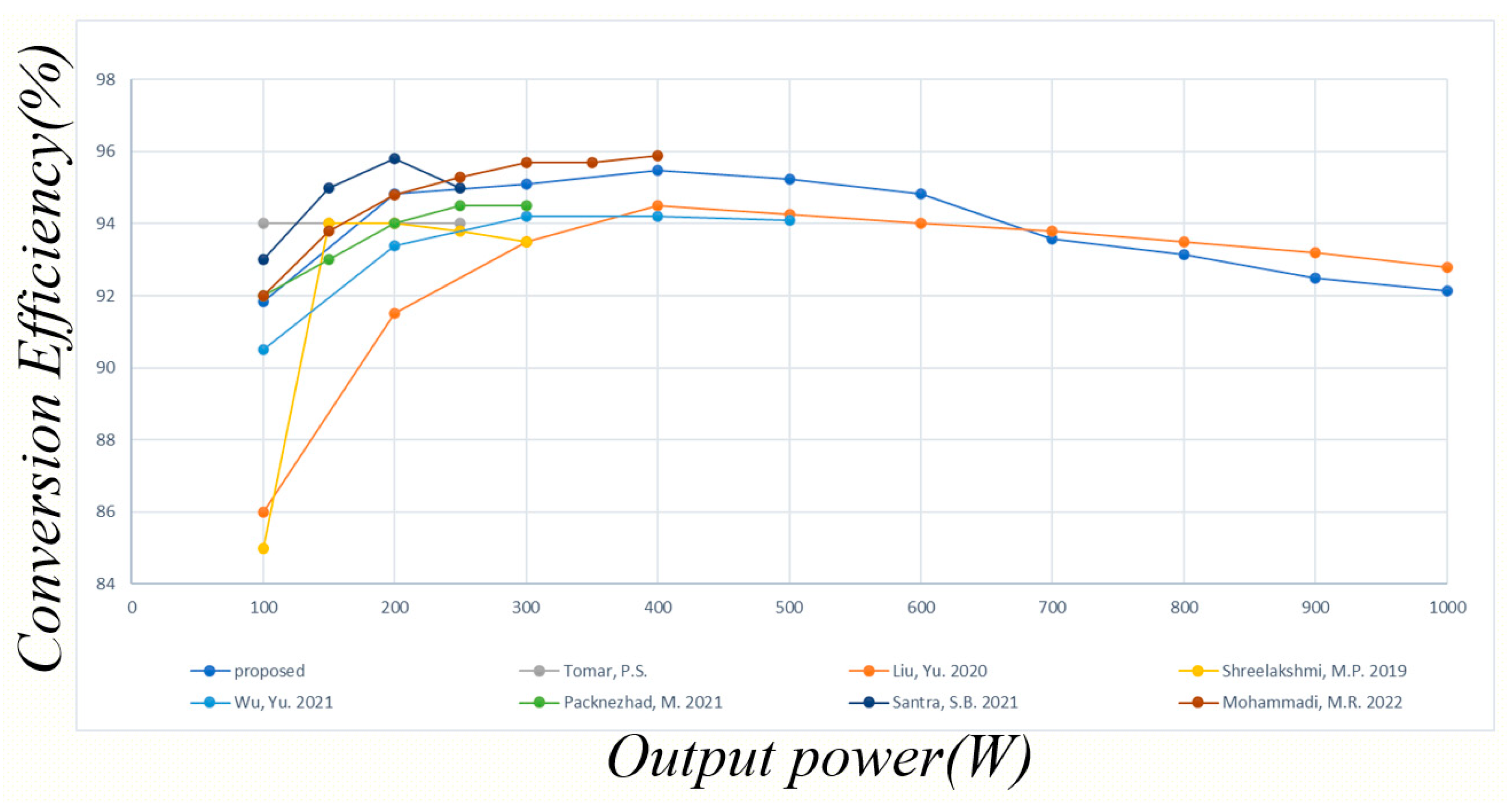
Figure 29 and Figure 30 present conversion efficiency comparisons between the proposed converter and the converters proposed in [20,21] and [23,24,25,26,27] operated in step-up and step-down modes, respectively. In the converter described in [20], the conversion efficiency was not high, and the output power of the converter was insufficient. Of all the converters, the converter in [21] has the highest switching frequency; this can greatly reduce converter size, but too many components lead to increased costs. In the converter described in [25], all switches have ZVS, but the efficiency is mediocre. The overall conversion efficiency is the highest in the converter described in [26], but the output power of this converter is insufficient for storage systems. In the converter described in [27], the PWM control signals are too complex.
In summary, the overall conversion efficiency of the proposed converter is high, and the converter has substantial power in both step-up and step-down modes. In addition, this converter has the widest input range of all the converters.
5. Conclusions
This study proposed a novel bidirectional isolated DC/DC converter with a high gain ratio and wide input voltage for EV storage systems. This converter only requires one complementary PWM output to control step-up and step-down modes. Partial switches achieve ZVS, which can increase efficiency. The topology proposed in this paper was demonstrated to be feasible through theoretical analysis and experimentation. When the power on the low-voltage side was 24, 48, and 58 V, the maximum efficiency in step-up mode was 95.1%, 96.5%, and 94.8%, respectively, and the maximum efficiency in step-down mode was 94.4%, 95.4%, and 93.6%, respectively.
The advantages of the proposed converter are as follows: (1) The circuit structure is simple. (2) The converter only requires one complementary PWM output. (3) The converter achieves a wide voltage gain and high voltage gain. (4) Galvanic isolation separates the input and output power supplies. (5) The current of the low-voltage side is continuous in CCM. (6) ZVS technology is used in specific switches to reduce switching loss.
Future research directions include: (1) The proposed topology can be designed for three-stage charging, which are bulk charge, absorption, and float charge to extend battery life effectively by adding current sensor. (2) Modularize the proposed topology to achieve multiple groups of bidirectional energy transmission in parallel to deal with the application of greater power. (3) Implement greater practical power.
Author Contributions
Conceptualization, Y.-E.W.; methodology, Y.-E.W. and C.-H.T.; formal analysis, Y.-E.W. and C.-H.T.; investigation, C.-H.T.; resources, Y.-E.W.; writing—original draft preparation, Y.-E.W. and C.-H.T.; writing—review and editing, Y.-E.W.; project administration, Y.-E.W.; funding acquisition, Y.-E.W. All authors have read and agreed to the published version of the manuscript.
Funding
This research received no external funding.
Data Availability Statement
All data utilized in this study are available online.
Conflicts of Interest
The authors declare no conflict of interest.
References
- Reilly, J.M.; Jacoby, H.D.; Prinn, R.G. Multi-gas contributors to global climate change. Mass. Inst. Technol. 2003, 10, 2–3. [Google Scholar]
- Available online: https://arstechnica.com/science/2020/12/battery-prices-have-fallen-88-percent-over-the-last-decade/ (accessed on 25 March 2021).
- Available online: https://www.electrical-energy-storage.events/en/news-press/news/articles?tx_news_pi1[news]=3203&cHash=079c662402bdfe836ee1d0305b02962aZ (accessed on 26 March 2021).
- Pradhan, R.; Subudhi, B. Double Integral Sliding Mode MPPT Control of a Photovoltaic System. IEEE Trans. Control Syst. Technol. 2016, 24, 285–292. [Google Scholar] [CrossRef]
- Messalti, S.; Harrag, A.G.; Loukriz, A.E. A new neural networks MPPT controller for PV systems. In Proceedings of the IREC2015 The Sixth International Renewable Energy Congress, Sousse, Tunisia, 24–26 March 2015; pp. 1–6. [Google Scholar]
- Raiker, G.A.; Loganathan, U.; Reddy, S. Current Control of Boost Converter for PV Interface with Momentum-Based Perturb and Observe MPPT. IEEE Trans. Ind. Appl. 2021, 57, 4071–4078. [Google Scholar] [CrossRef]
- Gang, L.H.L.; Jovanovic, M.M. Design-oriented analysis and performance evaluation of buck PFC front end. IEEE Trans. Power Electron. 2010, 25, 85–94. [Google Scholar]
- Amini, A.E.M.R.; Farzaneh-fard, H. Soft single switch resonant buck converter with inherent PFC feature. IET Power Electron. 2013, 6, 516–522. [Google Scholar]
- Ye, Z.; Sun, B. PFC efficency improvement and THD reduction at light loads with ZVS and valley switching. In Proceedings of the 2012 Twenty-Seventh Annual IEEE Applied Power Electronics Conference and Exposition (APEC), Orlando, FL, USA, 5–9 February 2012; pp. 802–806. [Google Scholar]
- Ai, J.; Lin, M.; Yin, M. A Family of High Step-Up Cascade DC–DC. IEEE Trans. Power Electron. 2020, 35, 4819–4834. [Google Scholar] [CrossRef]
- Cheng, H.; Chang, Y.; Yen, H.; Hua, C.; Su, P. An Interleaved Flyback-Typed LED Driver With ZVS and Energy Recovery of Leakage Inductance. IEEE Trans. Power Electron. 2019, 34, 4497–4508. [Google Scholar] [CrossRef]
- Wang, J.; Prodic, A.; Ng, W.T. Mixed-Signal-Controlled Flyback-TransformerBased Buck Converter With Improved DynamicPerformance and Transient Energy Recycling. IEEE Trans. Power Electron. 2013, 28, 970–983. [Google Scholar] [CrossRef]
- Hassan, W.; Soon, J.L.; Lu, D.D.; Xiao, W. A High Conversion Ratio and High-Efficiency Bidirectional DC–DC Converter With Reduced Voltage Stress. IEEE Trans. Power Electron. 2020, 35, 11828–11831. [Google Scholar] [CrossRef]
- Zhang, Y.; Liu, Q.; Li, J.; Sumner, M. A Common Ground Switched-Quasi-Z-Source Bidirectional DC–DC Converter With Wide-Voltage-Gain Range for EVs With Hybrid Energy Sources. IEEE Trans. Ind. Electron. 2018, 65, 5189–5191. [Google Scholar] [CrossRef]
- Gorji, S.A.; Sahebi2, H.G.; Ektesabi1, M.; Rad, A.B. Topologies and Control Schemes of Bidirectional DC–DC Power Converters: An Overview. IEEE Access 2019, 7, 118002–118003. [Google Scholar] [CrossRef]
- Ma, X.; Wang, P.; Bi, H.; Wang, Z. High-Efficiency Current-Fed Dual Active Bridge DC–DC Converter With ZVS Achievement Throughout Full Range of Load Using Optimized Switching Patterns. IEEE Access 2020, 8, 125549–125563. [Google Scholar] [CrossRef]
- Sha, D.; Wang, X.; Chen, D. High-Efficiency Current-Fed Dual Active Bridge DC–DC Converter With ZVS Achievement Throughout Full Range of Load Using Optimized Switching Patterns. IEEE Trans. Power Electron. 2018, 33, 1347–1357. [Google Scholar] [CrossRef]
- Zhu, L. A novel soft-commutating isolated boost full-bridge ZVS PWM dc-dc converter for bi-directional high power applications. In Proceedings of the IEEE Power Electronics Specialists Conf. (PESC’04), Aachen, Germany, 20–25 June 2004; pp. 2141–2146. [Google Scholar]
- Yaqoob, M.; Loo, K.; Lai, Y.M. Fully Soft-Switched Dual-Active-Bridge Series-Resonant Converter With Switched-Impedance-Based Power Control. IEEE Trans. Power Electron. 2018, 33, 9267–9281. [Google Scholar] [CrossRef]
- Tomar, P.S.; Srivastava, M.; Verma, A.K. An Improved Current-Fed Bidirectional DC–DC Converter for Reconfigurable Split Battery in EVs. IEEE Trans. Ind. Appl. 2020, 56, 6957–6966. [Google Scholar] [CrossRef]
- Liu, Y.; Chen, C.; Chen, K.; Syu, Y.; Dung, N.A. High-Frequency and High-Efficiency Isolated Two-Stage Bidirectional DC–DC Converter for Residential Energy Storage Systems. IEEE J. Emerg. Sel. Top. Power Electron. 2020, 8, 1994–2004. [Google Scholar] [CrossRef]
- Kim, N.; Jo, S.; Han, B.; Choi, H.; Kim, M. Highly Efficient Bidirectional Current-Fed Resonant Converter Over a Wide Voltage Gain Range. IEEE Trans. Ind. Electron. 2021, 68, 10913–10916. [Google Scholar] [CrossRef]
- Shreelakshmi, M.P.; Das, M.; Agarwal, V. Design and Development of a Novel High Voltage Gain, High-Efficiency Bidirectional DC–DC Converter for Storage Interface. IEEE Trans. Ind. Electron. 2019, 66, 4490–4501. [Google Scholar]
- Wu, Y.; Ke, Y. A Novel Bidirectional Isolated DC-DC Converter With High Voltage Gain and Wide Input Voltage. IEEE Trans. Power Electron. 2021, 36, 7973–7985. [Google Scholar] [CrossRef]
- Packnezhad, M.; Farzanehfard, H. Soft-Switching High Step-Up/Down Converter Using Coupled Inductors With Minimum Number of Components. IEEE Trans. Ind. Electron. 2021, 68, 7938–7945. [Google Scholar] [CrossRef]
- Santra, S.B.; Chatterjee, D.; Liang, T. High Gain and High-Efficiency Bidirectional DC–DC Converter With Current Sharing Characteristics Using Coupled Inductor. IEEE Trans. Power Electron. 2021, 36, 12819–12832. [Google Scholar] [CrossRef]
- Mohammadi, M.R.; Amoorezaei, A.; Khajehoddin, S.A.; Moez, K. A High Step-Up/Step-Down LVS-Parallel HVS-Series ZVS Bidirectional Converter With Coupled Inductors. IEEE Trans. Power Electron. 2022, 37, 1945–1961. [Google Scholar]
Figure 1.
Application of diverse converters with DC buses.

Figure 2.
Application of proposed bidirectional isolated DC/DC converter.

Figure 3.
Voltage polarity and current direction of components.

Figure 4.
Key waveform of proposed topology in step-up mode.

Figure 5.
Equivalent circuit in step-up mode. (a) Mode 1, (b) Mode 2, (c) Mode 3, (d) Mode 4, and (e) Mode 5.
Figure 5.
Equivalent circuit in step-up mode. (a) Mode 1, (b) Mode 2, (c) Mode 3, (d) Mode 4, and (e) Mode 5.

Figure 6.
Key waveforms of the proposed topology in step-down mode.

Figure 7.
Equivalent circuit in step-down mode. (a) Mode 1, (b) Mode 2, (c) Mode 3, (d) Mode 4, and (e) Mode 5.
Figure 7.
Equivalent circuit in step-down mode. (a) Mode 1, (b) Mode 2, (c) Mode 3, (d) Mode 4, and (e) Mode 5.

Figure 8.
Relationship between voltage gain and duty cycle in step-up mode.

Figure 9.
Voltage gain versus duty cycle in step-down mode.

Figure 10.
L1, BCM in step-up mode.

Figure 11.
Lm1, BCM in step-up mode.

Figure 12.
Photograph of the proposed converter.

Figure 13.
Closed-loop control scheme of the proposed converter.

Figure 14.
Experimental results for operation of the proposed converter at full load and at VL = 24 V in step-up mode. (a) Waveforms of vgs1,3,5, vgs2,4,6, iL1, and ilk1. (b) Waveforms of vgs1,3,5, vds1, and ids1 of S1. (c) Waveforms of vgs2,4,6, vds2, and ids2 of S2. (d) Waveforms of vgs1,3,5, vds3, and ids3 of S3. (e) Waveforms of vgs2,4,6, vds4, and ids4 of S4. (f) Waveforms of vds5 and ids5 of S5. (g) Waveforms of vds6 and ids6 of S6.

Figure 15.
Experimental results from operating the proposed converter at full load and at VL = 48 V in step-up mode. (a) Waveforms of vgs1,3,5, vgs2,4,6, iL1, and ilk1. (b) Waveforms of vgs1,3,5, vds1, and ids1 of S1. (c) Waveforms of vgs2,4,6, vds2, and ids2 of S2. (d) Waveforms of vgs1,3,5, vds3, and ids3 of S3. (e) Waveforms of vgs2,4,6, vds4, and ids4 of S4. (f) Waveforms of vds5 and ids5 of S5. (g) Waveforms of vds6 and ids6 of S6.

Figure 16.
Experimental results from operating the proposed converter at full load and at VL = 58 V in step-up mode. (a) Waveforms of vgs1,3,5, vgs2,4,6, iL1, and ilk1. (b) Waveforms of vgs1,3,5, vds1, and ids1 of S1. (c) Waveforms of vgs2,4,6, vds2, and ids2 of S2. (d) Waveforms of vgs1,3,5, vds3, and ids3 of S3. (e) Waveforms of vgs2,4,6, vds4, and ids4 of S4. (f) Waveforms of vds5 and ids5 of S5. (g) Waveforms of vds6 and ids6 of S6.

Figure 17.
Experimental results related to ZVS for one cycle at full load (1000 W) in step-up mode. (a) vds and ids of S3 and S4 at VL = 24 V. (b) vds and ids of S3 and S4 at VL = 48 V. (c) vds and ids of S3 and S4 at VL = 58 V.
Figure 17.
Experimental results related to ZVS for one cycle at full load (1000 W) in step-up mode. (a) vds and ids of S3 and S4 at VL = 24 V. (b) vds and ids of S3 and S4 at VL = 48 V. (c) vds and ids of S3 and S4 at VL = 58 V.

Figure 18.
Loss distribution for experiment under VL = 24 V, VH = 400 V, and P = 1000 W in step-up mode.
Figure 18.
Loss distribution for experiment under VL = 24 V, VH = 400 V, and P = 1000 W in step-up mode.

Figure 19.
Experimental results from operating the proposed converter at full load (1000 W) and at VL = 24 V in step-down mode. (a) Waveforms of vgs1,3,5, vgs2,4,6, iL1, and ilk1. (b) Waveforms of vgs1,3,5, vds1, and ids1 of S1. (c) Waveforms of vgs2,4,6, vds2, and ids2 of S2. (d) Waveforms of vgs1,3,5, vds3, and ids3 of S3. (e) Waveforms of vgs2,4,6, vds4, and ids4 of S4. (f) Waveforms of vgs1,3,5, vds5, and ids5 of S5. (g) Waveforms of vgs2,4,6, vds6, and ids6 of S6.

Figure 20.
Experimental results from operating the proposed converter at full load (1000 W) and at VL = 48 V in step-down mode. (a) Waveforms of vgs1,3,5, vgs2,4,6, iL1, and ilk1. (b) Waveforms of vgs1,3,5, vds1, and ids1 of S1. (c) Waveforms of vgs2,4,6, vds2, and ids2 of S2. (d) Waveforms of vgs1,3,5, vds3, and ids3 of S3. (e) Waveforms of vgs2,4,6, vds4, and ids4 of S4. (f) Waveforms of vgs1,3,5, vds5, and ids5 of S5. (g) Waveforms of vgs2,4,6, vds6, and ids6 of S6.

Figure 21.
Experimental results from operating the proposed converter at full load (1000 W) and at VL = 58 V in step-down mode. (a) Waveforms of vgs1,3,5, vgs2,4,6, iL1, and ilk1. (b) Waveforms of vgs1,3,5, vds1, and ids1 of S1. (c) Waveforms of vgs2,4,6, vds2, and ids2 of S2. (d) Waveforms of vgs1,3,5, vds3, and ids3 of S3. (e) Waveforms of vgs2,4,6, vds4, and ids4 of S4. (f) Waveforms of vgs1,3,5, vds5, and ids5 of S5. (g) Waveforms of vgs2,4,6, vds6, and ids6 of S6.

Figure 22.
Experimental results related to ZVS for one cycle at full load (1000 W) in step-down mode. (a) vds and ids of S5 and S6 at VL = 24 V. (b) vds and ids of S5 and S6 at VL = 48 V. (c) vds and ids of S5 and S6 at VL = 58 V.
Figure 22.
Experimental results related to ZVS for one cycle at full load (1000 W) in step-down mode. (a) vds and ids of S5 and S6 at VL = 24 V. (b) vds and ids of S5 and S6 at VL = 48 V. (c) vds and ids of S5 and S6 at VL = 58 V.

Figure 23.
Calculated loss distribution from experimentation under VL = 48 V, VH = 400 V, and P = 1000 W in step-down mode.
Figure 23.
Calculated loss distribution from experimentation under VL = 48 V, VH = 400 V, and P = 1000 W in step-down mode.

Figure 24.
Efficiency of proposed converter in step-up mode.

Figure 25.
Efficiency curve of the proposed converter in step-down mode.

Figure 26.
Step variation in output load in (a) step-up mode and (b) step-down mode.

Figure 27.
Comparison of voltage gain in step-up mode. In colorful order the references are [20], [26], [23], [27], [24], [25], and [21].

Figure 28.
Comparison of voltage gain in step-down mode. In colorful order the references are [20], [26], [23], [27], [24], [25], and [21].

Figure 29.
Efficiency comparison in step-up mode. In colorful order [20], [21], [23], [24], [25], [26], and [27].

Figure 30.
Efficiency comparison in step-down mode. In colorful order [20], [21], [23], [24], [25], [26], and [27].


Table 1.
Electrical specifications of proposed topology.
| Parameter | Specification |
|---|---|
| High-side power PH | 1000 W |
| Low-side power PL | 1000 W |
| High-side voltage VH | 400 V |
| Low-side voltage VL | 24–58 V |
| Switching frequency fs | 40 kHz |
| Power switches S1, S2, and S3 | IRFP4568PbF |
| Power switch S4 | IRFP4768PbF |
| Power switches S5 and S6 | IXFH50N50P3 |
| Inductor L1 | 47 μH |
| Magnetizing inductance Lm1 | 190 μH |
| Leakage inductance Llk1 | 2.4 μH |
| Capacitor C1 | 100 μF |
| Capacitor C2 | 70 μF |
| Capacitor C3 and C4 | 220 μF |
| Turns ratio N | 2.2 |
Table 2.
Comparison between the proposed converter and related bidirectional converters.
| Converter in [20] | Converter in [21] | Converter in [23] | Converter in [24] | Converter in [25] | Converter in [26] | Converter in [27] | Proposed Converter | |
|---|---|---|---|---|---|---|---|---|
| Voltage gain in step-up mode | ||||||||
| Voltage gain in step-down mode | ||||||||
| Vin | 24–48 V | 35–50 V | 40 V | 24–55 V | 48 V | 48 V | 48 V | 24–58 V |
| Vo | 360 V | 400 V | 400 V | 400 V | 380 V | 384 V | 400 V | 400 V |
| Switches | 4 | 10 | 4 | 6 | 3 | 6 | 4 | 6 |
| Inductors | 1 | 2 | 0 | 1 | 0 | 0 | 0 | 1 |
| Coupled inductor | 1 | 1 | 1 | 1 | 1 | 1 | 2 | 1 |
| Capacitors | 6 | 3 | 2 | 3 | 1 | 4 | 3 | 4 |
| Diodes | 0 | 0 | 0 | 0 | 0 | 0 | 3 | 0 |
| Output power | 250 W | 1000 W | 300 W | 500 W | 300 W | 250 W | 400 W | 1000 W |
| Efficiency of step-up mode | 94% | 94% | 94% | 96% | 94% | 96% | 95% | 96% |
| Efficiency of step-down mode | 93% | 94% | 94% | 94% | 95% | 96% | 95% | 95% |
| PWM Control Signals | Normal | Complex | Normal | Normal | Normal | Normal | complex | Normal |
| Isolated | Yes | Yes | No | Yes | No | No | No | Yes |
Publisher’s Note: MDPI stays neutral with regard to jurisdictional claims in published maps and institutional affiliations. |
© 2022 by the authors. Licensee MDPI, Basel, Switzerland. This article is an open access article distributed under the terms and conditions of the Creative Commons Attribution (CC BY) license (https://creativecommons.org/licenses/by/4.0/).
Share and Cite
MDPI and ACS Style
Wu, Y.-E.; Tai, C.-H. Novel Bidirectional Isolated DC/DC Converter with High Gain Ratio and Wide Input Voltage for Electric Vehicle Storage Systems. Batteries 2022, 8, 240. https://0-doi-org.brum.beds.ac.uk/10.3390/batteries8110240
AMA Style
Wu Y-E, Tai C-H. Novel Bidirectional Isolated DC/DC Converter with High Gain Ratio and Wide Input Voltage for Electric Vehicle Storage Systems. Batteries. 2022; 8(11):240. https://0-doi-org.brum.beds.ac.uk/10.3390/batteries8110240
Chicago/Turabian StyleWu, Yu-En, and Chen-Han Tai. 2022. "Novel Bidirectional Isolated DC/DC Converter with High Gain Ratio and Wide Input Voltage for Electric Vehicle Storage Systems" Batteries 8, no. 11: 240. https://0-doi-org.brum.beds.ac.uk/10.3390/batteries8110240
Note that from the first issue of 2016, this journal uses article numbers instead of page numbers. See further details here.