Common Phase and Structure Misidentifications in High-Resolution TEM Characterization of Perovskite Materials


Academy for Advanced Interdisciplinary Studies, Peking University, Beijing 100871, China
Condens. Matter 2021, 6(1), 1; https://0-doi-org.brum.beds.ac.uk/10.3390/condmat6010001
Submission received: 5 October 2020
/
Revised: 29 November 2020
/
Accepted: 25 December 2020
/
Published: 29 December 2020
Abstract
:High-resolution TEM (HRTEM) is a powerful tool for structure characterization. However, methylammonium lead iodide (MAPbI3) perovskite is highly sensitive to electron beams and easily decomposes into lead iodide (PbI2). Misidentifications, such as PbI2 being incorrectly labeled as perovskite, are widely present in HRTEM characterization and would negatively affect the development of perovskite research field. Here misidentifications in MAPbI3 perovskite are summarized, classified, and corrected based on low-dose imaging and electron diffraction (ED) simulations. Corresponding crystallographic parameters of intrinsic tetragonal MAPbI3 and the confusable hexagonal PbI2 are presented unambiguously. Finally, the method of proper phase identification and some strategies to control the radiation damage in HRTEM are provided. This warning paves the way to avoid future misinterpretations in HRTEM characterization of perovskite and other electron beam-sensitive materials.
1. Introduction
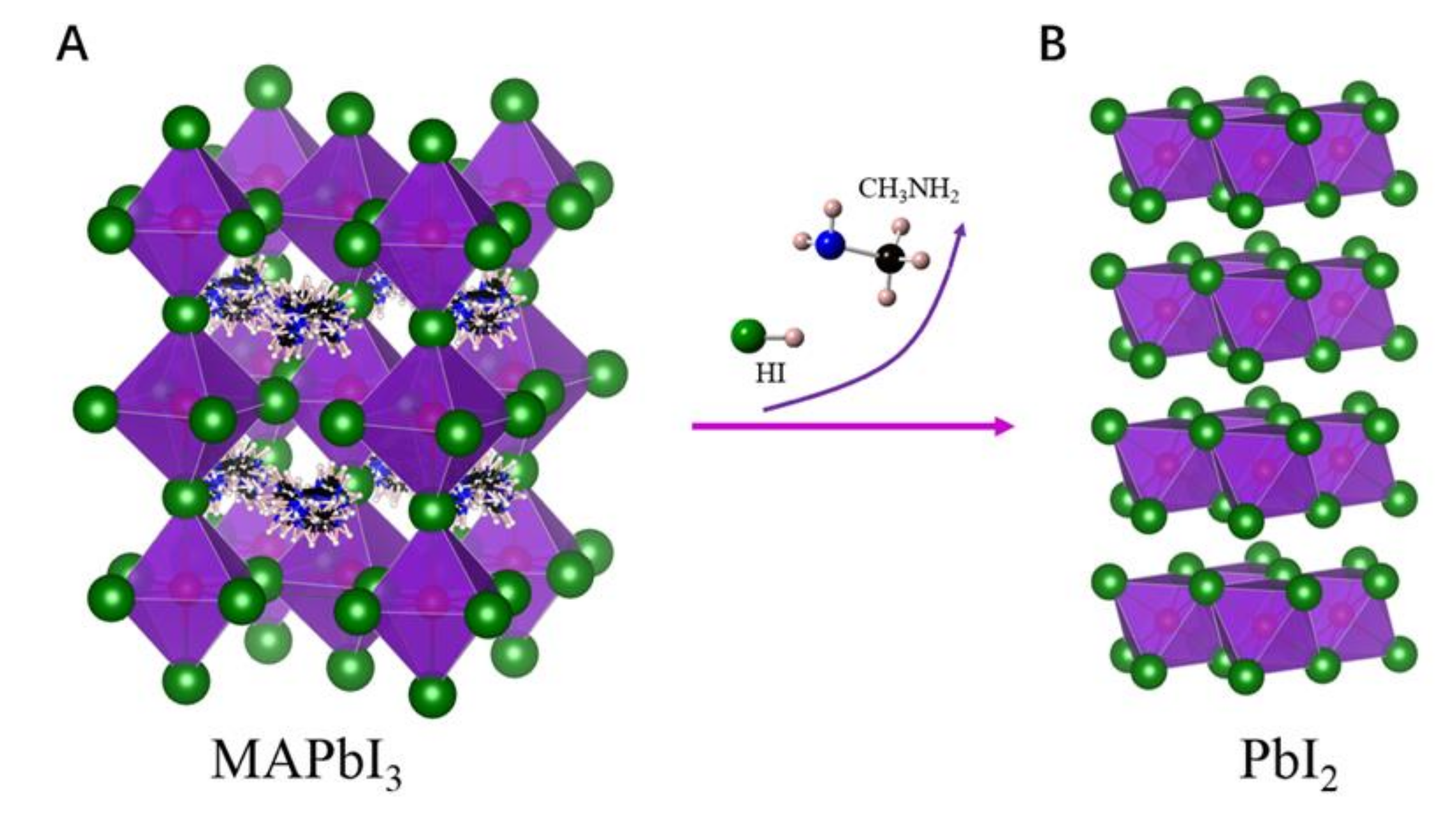
High-resolution transmission electron microscopy (HRTEM) is a powerful characterization tool and has been extensively and successfully used for analyzing crystal structures on an atomic scale [1,2,3,4]. Recently, halide perovskites have achieved substantial success in various optoelectronic devices owing to their solution-based growth and their remarkable physical properties [5,6,7,8,9]. However, the extensively studied methylammonium lead iodide (MAPbI3) perovskite is very sensitive to electron beam irradiation. Figure 1 shows the MAPbI3 degradation process under electron beam irradiation. Tetragonal perovskite decomposes into hexagonal lead iodide (PbI2) by the dissociation of methylamine and hydrogen iodide molecules.
Comparing distances and angles between crystal planes to identify the material phase, it is easy to ignore the missing crystal planes, which leads to false identification results, such as labelling lead iodide as perovskite. In a proper phase identification, HRTEM images alone cannot be used for phase identification, but always have to be supported by other measurement results such as diffractograms, simulated ED, nanodiffractions, or XRD specimen data [1]. As a rough estimation, MAPbI3 decomposes into PbI2 at a total dose irradiation > 150 eÅ−2 [10,11]. However, the value of the electron dose in normal HRTEM is around 800–2000 eÅ−2 s−1, so the experimental total dose would have been much higher than the critical dose of MAPbI3 perovskite. Meanwhile, distances and angles between crystal planes in the decomposition product PbI2 are very similar to MAPbI3, such that PbI2 can easily be misidentified as perovskite. A typical feature of such misidentification is missing crystal planes in the results. Therefore, the absence of crystal planes serves as an indicator that the material is not in the perovskite, but another structural phase.
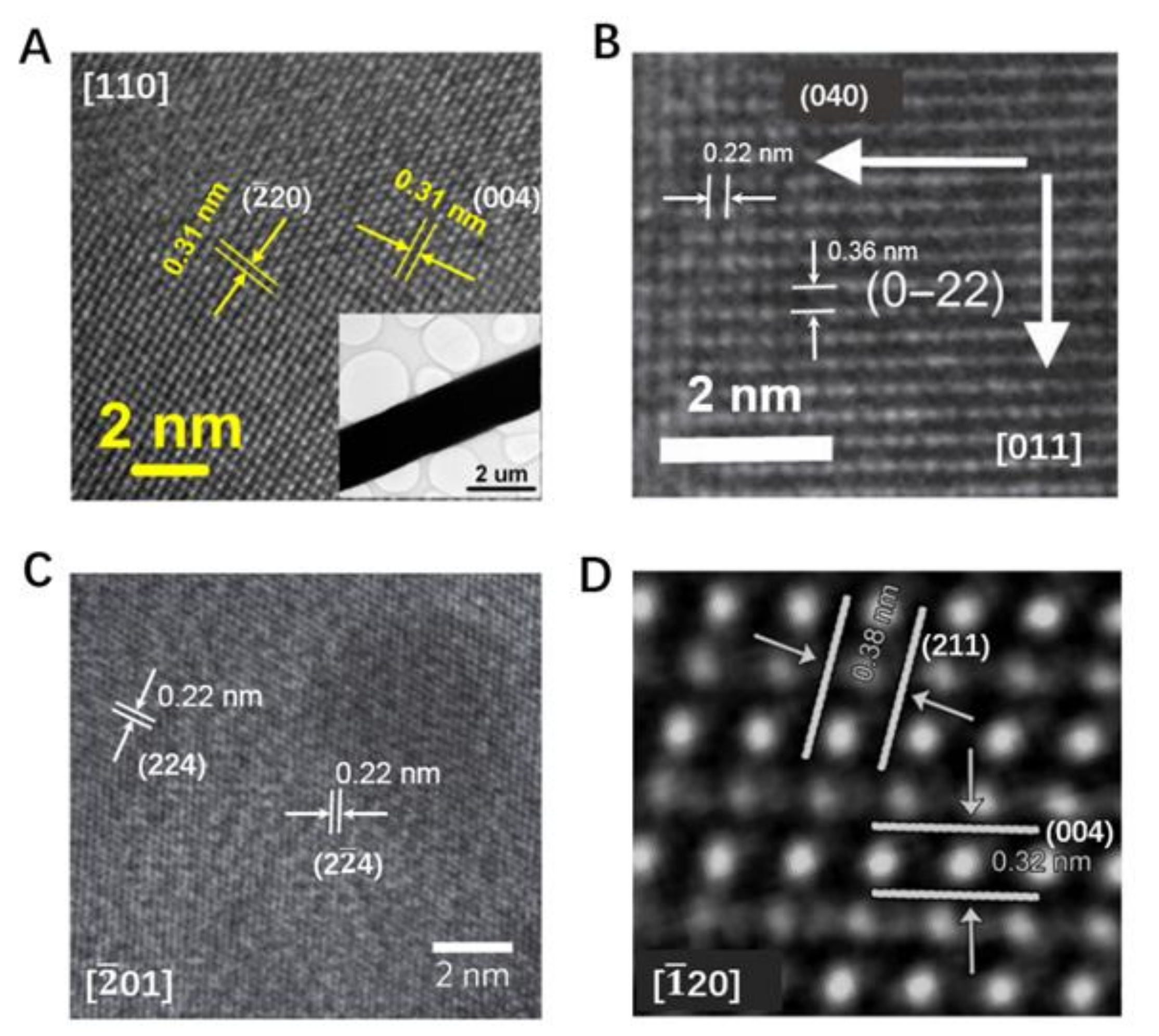
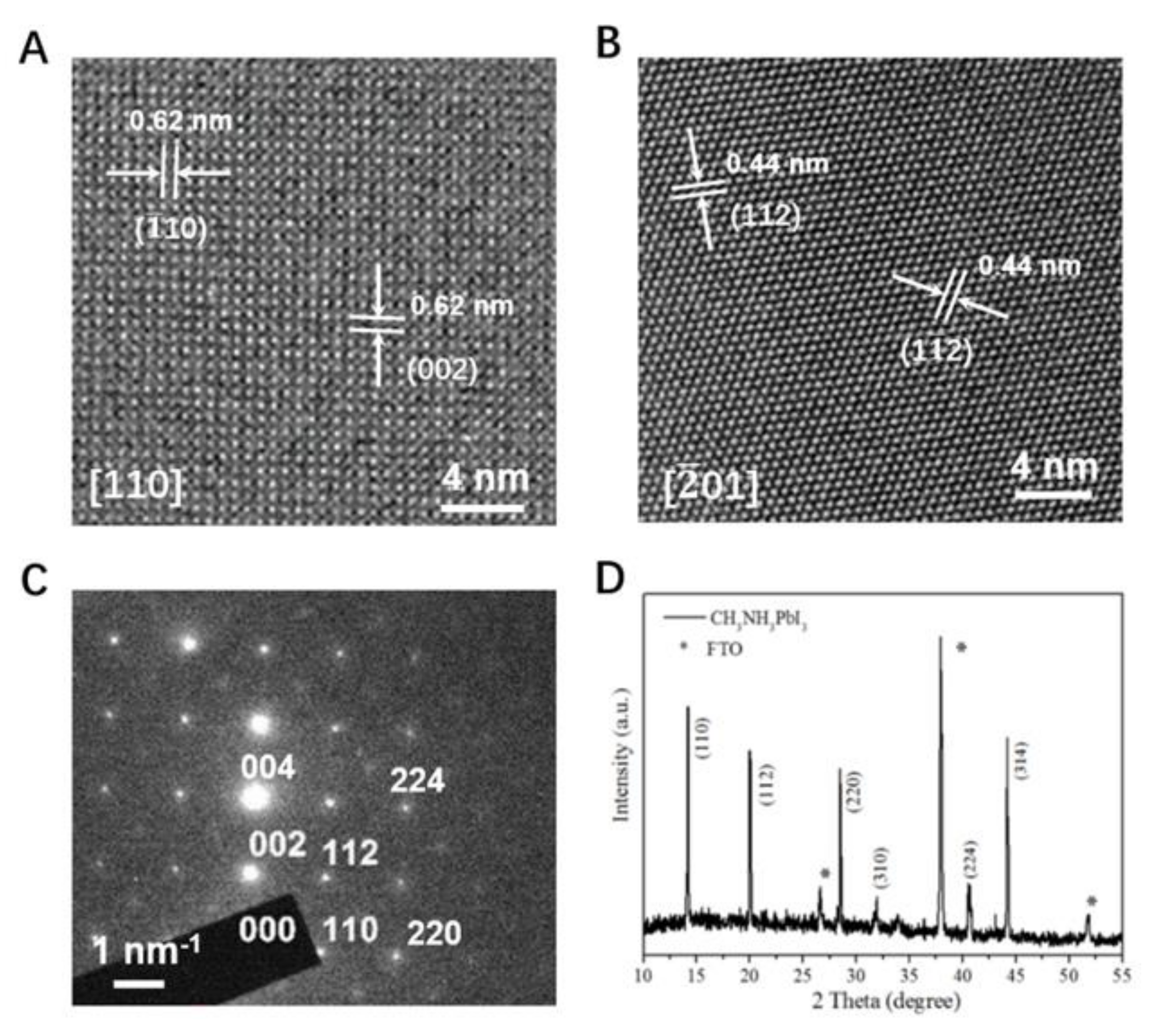
Such misidentifications were widely ignored in literature studies [9,12,13,14,15,16,17,18,19,20,21,22,23,24,25,26,27,28,29,30,31]. Figure 2 shows typical HRTEM images with missing crystal planes. (10), (002) planes are missing along the [110] zone axis (Figure 2A) [21], (020) plane is missing along the [101] zone axis (Figure 2B) [27], (11), (112) planes are missing along the [01] zone axis (Figure 2C) [13], and (002) plane is missing along the [20] zone axis (Figure 2D) [28]. However, missing crystal planes have been observed in low-dose imaging. Thus far, Song et al. have observed the missing (10), (002) planes with 0.63 nm along [110] zone axis at total doses of 1.5 eÅ−2 (Figure 3A) [32]. Similarly, Zhu et al. have observed the missing (12), (112) planes with 0.44 nm along the [01] zone axis by Cryo-TEM at a low electron dose of about 3 e Å-2 (Figure 3B) [33]. Moreover, the missing crystal planes have also been observed in other characterization techniques based on the Bragg’s law, such as selected area electron diffraction (SEAD) (Figure 3C) [34] and X-ray diffraction (XRD) (Figure 3D) [10,35,36,37]. Finally, the low-order crystal plane (d(112) = 4.4 Å) has longer interplanar spacing than the high-order crystal plane (d(224) = 2.2 Å). Thus, the missing of low-order crystal planes should not result from the poor accuracy in the data interpretation. Although the mistakes are taken seriously [10,11,35], an urgently needed, complete summary and correction of that issue has not been published yet.
2. Results and Discussion
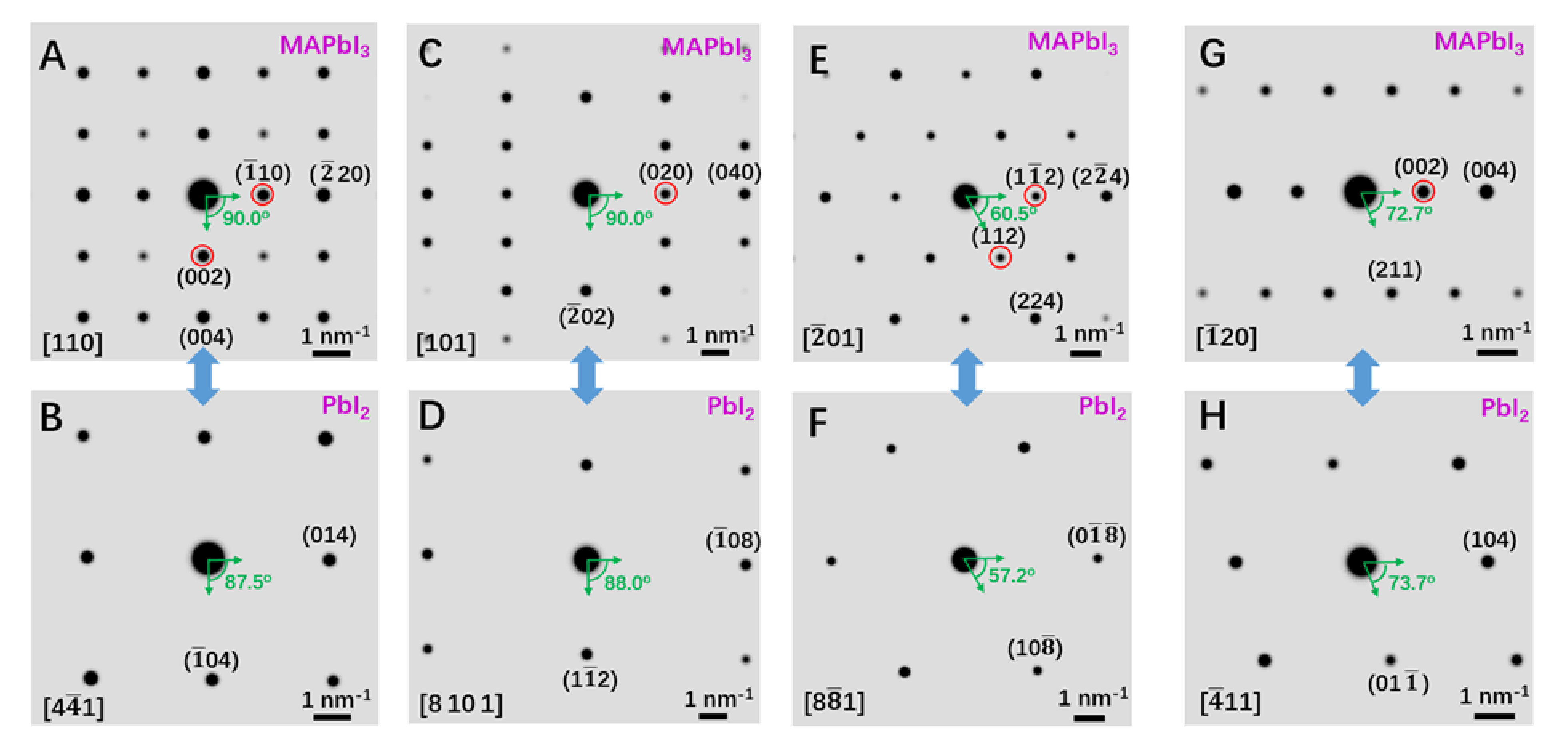
Here misidentifications in MAPbI3 perovskite are summarized, classified and corrected. Figure 4 shows simulated ED patterns of MAPbI3 and PbI2 along different axis zones. Figure 4A is the ED pattern of MAPbI3 along [110] zone axis. (10), (002) crystal planes are present in intrinsic tetragonal perovskite, but they are missing in a number of HRTEM characterizations [12,13,14,15]. Figure 4B shows the simulated ED patterns of PbI2 along [41] zone axis. (014), (04) crystal planes of PbI2 have the similar distances and angles between crystal planes compared to (0), (004) crystal planes of MAPbI3. In the actual experiment, MAPBI3 would decompose into PBI2 and the missing crystal planes would be oftentimes ignored, leading to aforementioned mischaracterizations. Similarly, Figure 4C–H show ED patterns of MAPbI3 along [101] and PbI2 along [8 10 1], MAPbI3 along [01] and PbI2 along [81], MAPbI3 along [20] and PbI2 along [11], respectively. The missing crystal planes in HRTEM characterizations are indicated by red circles in Figure 4.
Misidentifications exist in the following fields: phase identification and structure determination [16], grain, nanowire, and microwire orientation [9,14,17,18,19], morphology analysis and shape control of nanocrystals [20], growth direction of perovskite materials [21], degradation process and kinetics of perovskite [22], phase transition research in perovskite [26], and ion migration characterization in photoelectric devices [27]. Misidentifications not only occur in single component materials, but also in heterostructures, such as lattice matching and kinetic study in epitaxial growth of perovskite films on 2D materials [25], PbS quantum dots in perovskite materials [12,13], and lattice-anchoring stabilized perovskite research [14]. HRTEM is an auxiliary tool to identify the phase of perovskite materials and misinterpretations would not influence their device performances and conclusions. However, in some cases, such as the growth direction, orientation, and lattice matching of perovskite materials, misinterpretations in HRTEM would result in wrong conclusions. To make the comparisons and corrections clearer, Table 1 shows the detailed parameters of the intrinsic MAPbI3 and confusable PbI2 along different zone axis, where missing crystal planes are marked in red. Remarkably, the [110] and [001] zone axes are equivalent in tetragonal MAPbI3 perovskite.
The MAPbI3 perovskite is extremely beam-sensitive with a critical dose around a few hundred electrons per square angstrom. For most measurements, and in particular HRTEM, keeping the dose below the critical value is extremely challenging [38,39,40]. However, there are some ways to reduce the radiation damage in HRTEM, which might be helpful in obtaining the intrinsic structure of perovskite materials. Low-dose imaging techniques are effective approaches for electron beam-sensitive materials [41]. Zhang et al. developed a program to achieve a direct, one-step alignment of the zone axis and obtained HRTEM images of electron beam-sensitive materials with a dose of 6–12 e Å−2 [42]. Carlino reported the in-line holography in TEM for the study of radiation-sensitive materials providing high-contrast holograms within 1–2 eÅ−2s−1 [43]. The intrinsic structure of MAPbI3 has been captured by the Direct-detection electron-counting (DDEC) cameras at doses below 3 e Å−2 [33,44]. Cooling the specimen also poses a feasible way to reduce damage. Using Cryo-TEM, HRTEM images of MAPbI3 has been captured [11,33]. Lastly, encapsulation of specimen with a thin, stable, and continuous layer reduces radiation damage [40]. In any case, the total electron dose should be below the critical dose of MAPbI3, otherwise substantial damage occurs during TEM characterizations.
3. Conclusions
The MAPbI3 perovskite is very sensitive to electron beam irradiation and easily decomposes into PbI2. HRTEM characterizations performed above the critical dose can easily lead to misinterpretations, falsely identifying decomposition products as the actual perovskite. An indicator of such confusable decomposition products is missing crystal planes when comparing the expected theoretical diffractograms to the actual experimental data of MAPbI3. The summarized and analyzed misidentifications in HRTEM characterization of MAPbI3 may be helpful for researchers to avoid such misidentifications in perovskite research. Our findings show that it is unreliable to identify material phases only by measuring distances and angles between crystal planes. We need to take diffractograms, simulated ED, nanodiffractions, or XRD data into consideration in order to ensure complete crystal planes. We also provide a method of proper phase identification and some strategies to reduce the radiation damage in HRTEM.
4. Methods
Corresponding crystal structures cif files were downloaded from Crystallography Open Database (COD) website. COD IDs of MAPbI3 and PbI2 are 4124388 and 9009141 respectively [45,46]. MAPbI3 is I4/mcm space group with tetragonal structure, cell parameters: a = b = 8.839Å, c = 12.695Å; α = β = γ = 90°. PbI2 is P-3m1 space group with hexagonal structure, cell parameters: a = b = 4.555Å, c = 20.937Å; α = β = 90°, γ = 120°. The electron diffraction (ED) simulations of MAPbI3 and PbI2 were obtained using CrystalMaker Software. The interplanar spacings and interplanar angles can be calculated from the cell parameters. During the process of phase identification, we also tried other polytypes of PbI2, but the results did not match well.
Funding
This research received no external funding.
Data Availability Statement
All data are available from the corresponding author upon reasonable request.
Acknowledgments
The authors thank anonymous reviewers, academic editors and Leon Georg Nest for helpful suggestions and assistant editors for communications. The authors also appreciate the encouragements from Ying Xiong, Shulin Chen and Leon Georg Nest.
Conflicts of Interest
The author declares no competing financial interest.
References
- Spence, J.C.H. High-Resolution Electron Microscopy; OUP Oxford: Oxford, UK, 2013. [Google Scholar]
- Jia, C.L.; Lentzen, M.; Urban, K. Atomic-resolution imaging of oxygen in perovskite ceramics. Science 2003, 299, 870–873. [Google Scholar] [CrossRef] [PubMed] [Green Version]
- Pennycook, S.J.; Li, C.; Li, M.; Tang, C.; Okunishi, E.; Varela, M.; Kim, Y.-M.; Jang, J.H. Material structure, properties, and dynamics through scanning transmission electron microscopy. J. Anal. Sci. Technol. 2018, 9, 11. [Google Scholar] [CrossRef] [Green Version]
- Krivanek, O.; Chisholm, M.F.; Nicolosi, V.; Pennycook, T.J.; Corbin, G.J.; Dellby, N.; Murfitt, M.F.; Own, C.S.; Szilagyi, Z.S.; Oxley, M.P.; et al. Atom-by-atom structural and chemical analysis by annular dark-field electron microscopy. Nature 2010, 464, 571–574. [Google Scholar] [CrossRef] [PubMed] [Green Version]
- Best Research-Cell Efficiencies. National Renewable Energy Laboratory. Available online: https://www.nrel.gov/pv/cell-efficiency.html (accessed on 15 October 2020).
- Lin, K.; Xing, J.; Na Quan, L.; De Arquer, F.P.G.; Gong, X.; Lu, J.; Xie, L.; Zhao, W.; Zhang, D.; Yan, C.; et al. Perovskite light-emitting diodes with external quantum efficiency exceeding 20 per cent. Nature 2018, 562, 245–248. [Google Scholar] [CrossRef] [PubMed]
- Yang, Z.; Deng, Y.; Zhang, X.; Wang, S.; Chen, H.; Yang, S.; Khurgin, J.; Fang, N.X.; Zhang, X.; Ma, R.-M. High-Performance Single-Crystalline Perovskite Thin-Film Photodetector. Adv. Mater. 2018, 30, 1704333. [Google Scholar] [CrossRef]
- Deng, Y.H.; Yang, Z.Q.; Ma, R.M. Growth of centimeter-scale perovskite single-crystalline thin film via surface engineering. Nano Converg. 2020, 7, 1–7. [Google Scholar] [CrossRef]
- Zhu, H.; Fu, Y.; Meng, F.; Wu, X.; Gong, Z.; Ding, Q.; Gustafsson, M.V.; Trinh, M.T.; Jin, S.; Zhu, X.-Y. Lead halide perovskite nanowire lasers with low lasing thresholds and high quality factors. Nat. Mater. 2015, 14, 636–642. [Google Scholar] [CrossRef]
- Chen, S.; Zhang, X.; Zhao, J.; Zhang, Y.; Kong, G.; Li, Q.; Li, N.; Yu, Y.; Xu, N.; Zhang, J.; et al. Atomic scale insights into structure instability and decomposition pathway of methylammonium lead iodide perovskite. Nat. Commun. 2018, 9, 1–8. [Google Scholar]
- Li, Y.; Zhou, W.; Li, Y.; Huang, W.; Zhang, Z.; Chen, G.; Wang, H.; Wu, G.-H.; Rolston, N.; Vila, R.; et al. Unravelling degradation mechanisms and atomic structure of organic-inorganic halide perovskites by cryo-EM. Joule 2019, 3, 2854–2866. [Google Scholar] [CrossRef]
- Ning, Z.; Gong, X.; Comin, R.; Walters, G.; Fan, F.; Voznyy, O.; Yassitepe, E.; Buin, A.K.; Hoogland, S.; Sargent, E.H. Quantum-dot-in-perovskite solids. Nature 2015, 523, 324–328. [Google Scholar] [CrossRef]
- Gong, X.; Yang, Z.; Walters, G.; Comin, R.; Ning, Z.; Beauregard, E.; Adinolfi, V.; Voznyy, O.; Sargent, E.H. Highly efficient quantum dot near-infrared light-emitting diodes. Nat. Photonics 2016, 10, 253–257. [Google Scholar] [CrossRef]
- Liu, M.; Chen, Y.; Tan, C.-S.; Quintero-Bermudez, R.; Proppe, A.H.; Munir, R.; Tan, H.; Voznyy, O.; Scheffel, B.; Walters, G.; et al. Lattice anchoring stabilizes solution-processed semiconductors. Nature 2019, 570, 96–101. [Google Scholar] [CrossRef] [PubMed]
- Son, D.-Y.; Lee, J.-W.; Choi, Y.J.; Jang, I.-H.; Lee, S.; Yoo, P.J.; Shin, H.; Ahn, N.; Choi, M.; Kim, D.; et al. Self-formed grain boundary healing layer for highly efficient CH 3 NH 3 PbI 3 perovskite solar cells. Nat. Energy 2016, 1, 1–8. [Google Scholar]
- Yang, M.; Zhou, Y.; Zeng, Y.; Jiang, C.; Padture, N.P.; Zhu, K. Square-centimeter solution-processed planar CH3NH3PbI3 perovskite solar cells with efficiency exceeding 15%. Adv. Mater. 2015, 27, 6363–6370. [Google Scholar] [CrossRef] [PubMed]
- Xiao, M.; Huang, F.; Huang, W.; Dkhissi, Y.; Zhu, Y.; Etheridge, J.; Gray-Weale, A.; Bach, U.; Cheng, Y.-B.; Spiccia, L. A fast deposition-crystallization procedure for highly efficient lead iodide perovskite thin-film solar cells. Angew. Chem. Int. Ed. 2014, 53, 9898–9903. [Google Scholar] [CrossRef]
- Yang, B.; Dyck, O.; Poplawsky, J.; Keum, J.; Das, S.; Puretzky, A.; Aytug, T.; Joshi, P.C.; Rouleau, C.M.; Duscher, G.; et al. Controllable Growth of Perovskite Films by Room-Temperature Air Exposure for Efficient Planar Heterojunction Photovoltaic Cells. Angew. Chem. Int. Ed. 2015, 54, 14862–14865. [Google Scholar] [CrossRef]
- Li, S.; Li, Y.; Shi, Z.; Lei, L.; Ji, H.; Wu, D.; Xu, T.; Li, X.; Du, G. Fabrication of morphology-controlled and highly-crystallized perovskite microwires for long-term stable photodetectors. Sol. Energy Mater. Sol. Cells 2019, 191, 275–282. [Google Scholar] [CrossRef]
- Zhu, F.; Men, L.; Guo, Y.; Zhu, Q.; Bhattacharjee, U.; Goodwin, P.M.; Petrich, J.W.; Smith, E.A.; Vela, J. Shape evolution and single particle luminescence of organometal halide perovskite nanocrystals. ACS Nano 2015, 9, 2948–2959. [Google Scholar] [CrossRef]
- Gao, L.; Zeng, K.; Guo, J.; Ge, C.; Du, J.; Zhao, Y.; Chen, C.; Deng, H.; Haisheng, S.; Song, H.; et al. Passivated single-crystalline CH3NH3PbI3 nanowire photodetector with high detectivity and polarization sensitivity. Nano Lett. 2016, 16, 7446–7454. [Google Scholar] [CrossRef]
- Fan, Z.; Xiao, H.; Wang, Y.; Zhao, Z.; Lin, Z.; Cheng, H.-C.; Lee, S.-J.; Wang, G.; Feng, Z.; Goddard, I.W.A.; et al. Layer-by-layer degradation of methylammonium lead tri-iodide perovskite microplates. Joule 2017, 1, 548–562. [Google Scholar] [CrossRef] [Green Version]
- Li, D.; Wang, G.; Cheng, H.-C.; Chen, C.-Y.; Wu, H.; Liu, Y.; Huang, Y.; Duan, X. Size-dependent phase transition in methylammonium lead iodide perovskite microplate crystals. Nat. Commun. 2016, 7, 1–8. [Google Scholar] [CrossRef] [PubMed]
- Kim, S.; Bae, S.; Lee, S.-W.; Cho, K.; Lee, K.D.; Kim, H.; Park, S.; Kwon, G.; Ahn, S.-W.; Lee, H.-M.; et al. Relationship between ion migration and interfacial degradation of CH3NH3PbI3 perovskite solar cells under thermal conditions. Sci. Rep. 2017, 7, 1–9. [Google Scholar] [CrossRef] [PubMed] [Green Version]
- Tang, G.; You, P.; Tai, Q.; Yang, A.; Cao, J.; Zheng, F.; Zhou, Z.; Zhao, J.; Chan, P.K.L.; Yan, F. Solution-Phase Epitaxial Growth of Perovskite Films on 2D Material Flakes for High-Performance Solar Cells. Adv. Mater. 2019, 31, 1807689. [Google Scholar] [CrossRef] [PubMed]
- Kim, T.W.; Uchida, S.; Matsushita, T.; Cojocaru, L.; Jono, R.; Kimura, K.; Matsubara, D.; Shirai, M.; Ito, K.; Matsumoto, H.; et al. Self-Organized Superlattice and Phase Coexistence inside Thin Film Organometal Halide Perovskite. Adv. Mater. 2018, 30, 1705230. [Google Scholar] [CrossRef]
- Wang, G.; Li, D.; Cheng, H.C.; Li, Y.; Chen, C.-Y.; Yin, A.; Zhao, Z.; Lin, Z.; Wu, H.; He, Q.; et al. Wafer-scale growth of large arrays of perovskite microplate crystals for functional electronics and optoelectronics. Sci. Adv. 2015, 1, e1500613. [Google Scholar] [CrossRef] [PubMed] [Green Version]
- Niu, L.; Liu, X.; Cong, C.; Wu, C.; Wu, D.; Chang, T.R.; Wang, H.; Zeng, Q.; Zhou, J.; Wang, X.; et al. Controlled synthesis of organic/inorganic Van der waals solid for tunable light–matter interactions. Adv. Mater. 2015, 27, 7800–7808. [Google Scholar] [CrossRef] [PubMed]
- Liu, X.; Niu, L.; Wu, C.; Cong, C.; Wang, H.; Zeng, Q.; He, H.; Fu, Q.; Fu, W.; Yu, T.; et al. Periodic Organic–Inorganic Halide Perovskite Microplatelet Arrays on Silicon Substrates for Room-Temperature Lasing. Adv. Sci. 2016, 3, 1600137. [Google Scholar] [CrossRef] [Green Version]
- Kim, T.W.; Shibayama, N.; Cojocaru, L.; Uchida, S.; Kondo, T.; Segawa, H. Real-time in situ observation of microstructural change in organometal halide perovskite induced by thermal degradation. Adv. Funct. Mater. 2018, 28, 1804039. [Google Scholar] [CrossRef]
- Zhao, J.; Kong, G.; Chen, S.; Li, Q.; Huang, B.; Liu, Z.; San, X.; Wang, Y.; Wang, C.; Zhen, Y.; et al. Single crystalline CH3NH3PbI3 self-grown on FTO/TiO2 substrate for high efficiency perovskite solar cells. Sci. Bull. 2017, 62, 405–418. [Google Scholar] [CrossRef] [Green Version]
- Song, K.; Liu, L.; Zhang, D.; Hautzinger, M.P.; Jin, S.; Han, Y. Atomic-Resolution Imaging of Halide Perovskites Using Electron Microscopy. Adv. Energy Mater. 2020, 10, 1904006. [Google Scholar] [CrossRef]
- Zhu, Y.; Guia, Z.; Wang, Q.; Meng, F.; Feng, S.; Han, B.; Wang, P.; Huang, L.; Wang, H.-L.; Gu, M.; et al. Direct atomic scale characterization of the surface structure and planar defects in the organic-inorganic hybrid CH3NH3PbI3 by Cryo-TEM. Nano Energy 2020, 73, 104820. [Google Scholar] [CrossRef]
- Rothmann, M.U.; Li, W.; Zhu, Y.; Liu, A.; Ku, Z.; Bach, U.; Etheridge, J.; Cheng, Y. Structural and chemical changes to CH3NH3PbI3 induced by electron and gallium ion beams. Adv. Mater. 2018, 30, 1800629. [Google Scholar] [CrossRef] [PubMed]
- Dong, Q.; Fang, Y.; Shao, Y.; Mulligan, P.; Qiu, J.; Cao, L.; Huang, J. Electron-hole diffusion lengths 175 μm in solution-grown CH3NH3PbI3 single crystals. Science 2015, 347, 967–970. [Google Scholar] [CrossRef] [PubMed] [Green Version]
- Shi, D.; Adinolfi, V.; Comin, R.; Yuan, M.; Alarousu, E.; Buin, A.K.; Chen, Y.; Hoogland, S.H.; Rothenberger, A.; Katsiev, K.; et al. Low trap-state density and long carrier diffusion in organolead trihalide perovskite single crystals. Science 2015, 347, 519–522. [Google Scholar] [CrossRef] [PubMed] [Green Version]
- Zhang, X.W.; Yang, Z.Q.; Li, J.Z.; Deng, Y.H.; Hou, Y.M.; Mao, Y.F.; Lu, J.; Ma, R.M. Directly imaging the structure–property correlation of perovskites in crystalline microwires. J. Mater. Chem. A 2019, 7, 13305–13314. [Google Scholar] [CrossRef]
- Egerton, R.F. Outrun radiation damage with electrons? Adv. Struct. Chem. Imaging 2015, 1, 1–11. [Google Scholar] [CrossRef] [Green Version]
- Egerton, R.F. Control of radiation damage in the TEM. Ultramicroscopy 2013, 127, 100–108. [Google Scholar] [CrossRef]
- Egerton, R.F. Radiation damage to organic and inorganic specimens in the TEM. Micron 2019, 119, 72–87. [Google Scholar] [CrossRef]
- Egerton, R.F.; Qian, H. Exploiting the Dose-Rate Dependence of Radiolysis–a Future for Cryo-STEM? Microsc. Microanal. 2019, 25, 992–993. [Google Scholar] [CrossRef] [Green Version]
- Zhang, D.; Zhu, Y.; Liu, L.; Ying, X.; Hsiung, C.-E.; Sougrat, R.; Li, K.; Han, Y. Atomic-resolution transmission electron microscopy of electron beam–sensitive crystalline materials. Science 2018, 359, 675–679. [Google Scholar] [CrossRef] [Green Version]
- Carlino, E. In-Line Holography in Transmission Electron Microscopy for the Atomic Resolution Imaging of Single Particle of Radiation-Sensitive Matter. Materials 2020, 13, 1413. [Google Scholar] [CrossRef] [PubMed] [Green Version]
- Chen, S.; Zhang, Y.; Zhao, J.; Mi, Z.; Zhang, J.; Cao, J.; Feng, J.; Zhang, G.; Qi, J.; Li, J.; et al. Transmission electron microscopy of organic-inorganic hybrid perovskites: Myths and truths. Sci. Bull. 2020. [Google Scholar] [CrossRef]
- COD of MAPbI3 (4124388). University of Cambridge. Available online: http://www.crystallography.net/cod/4124388.html (accessed on 15 October 2020).
- COD of PbI2 (9009141). University of Cambridge. Available online: http://www.crystallography.net/cod/9009141.html (accessed on 15 October 2020).
Figure 1.
MAPbI3 degradation under electron beam irradiation. Tetragonal perovskite (A) decomposes into hexagonal lead iodide (B) via dissociation of methylamine and hydrogen iodide molecules. Here, colors represent the following: green, iodine; red, lead; black, carbon; blue, nitrogen; pink, hydrogen.

Figure 2.
Typical HRTEM images with missing crystal planes. (A) (10), (002) planes are missing along the [110] zone axis. (B) (020) plane is missing along the [101] zone axis (Figure 2B). (C) (11), (112) planes are missing along the [01] zone axis. (D) (002) plane is missing along the [20] zone axis. (A) Reprinted with permission from Ref. [21], © American Chemical Society 2016. (B) Reproduced with permission from Ref. [27]. (C) Reprinted by permission from Springer Customer Service Centre GmbH: Springer Nature, Nature Photonics Gong et al., Highly efficient quantum dot near-infrared light-emitting diodes, © 2016. (D) Reproduced with permission from Ref. [28], © WILEY-VCH Verlag GmbH & Co. KGaA, Weinheim, Germany, 2015.

Figure 3.
Intrinsic MAPbI3 with complete crystal planes. (A) (10), (002) planes along [110] zone axis were observed at total doses of 1.5 eÅ-2. (B) (11), (112) planes along the [01] zone axis were observed by Cryo-TEM at a low electron dose of about 3 e Å-2. (C) Selected area electron diffraction (SEAD) of MAPbI3 perovskite. (D) X-ray diffraction (XRD) of MAPbI3 perovskite. (A) Reproduced with permission from Ref. [32], © WILEY-VCH Verlag GmbH & Co. KGaA, Weinheim, Germany, 2020. (B) Reproduced with permission from Ref. [33], © 2020 Elsevier B.V. 2020. (C) Reproduced with permission from Ref. [34], © WILEY-VCH Verlag GmbH & Co. KGaA, Weinheim, Germany, 2018. (D) Reproduced with permission from Ref. [10], © Springer Nature 2018.

Figure 4.
Simulated electron diffraction (ED) patterns of tetragonal MAPbI3 and hexagonal PbI2. (A) MAPbI3 along [110] axis zone. (B) PbI2 along [41] zone axis. (C) MAPbI3 along [101] axis zone. (D) PbI2 along [8 10 1] zone axis. (E) MAPbI3 along [01] zone axis. (F) PbI2 along [81] zone axis. (G) MAPbI3 along [20] zone axis. (H) PbI2 along [11] zone axis. Crystal planes marked in red circle are missing in published articles [9,12,13,14,15,16,17,18,19,20,21,22,23,24,25,26,27,28,29,30,31].


Table 1.
Detailed crystallographic parameters of MAPbI3 and PbI2 along different zone axes corresponding to Figure 4, the missing low-order crystal planes of MAPbI3 are marked in red. The similar crystal angles and interplanar spacings make them to be easily confused.
Table 1.
Detailed crystallographic parameters of MAPbI3 and PbI2 along different zone axes corresponding to Figure 4, the missing low-order crystal planes of MAPbI3 are marked in red. The similar crystal angles and interplanar spacings make them to be easily confused.
| Material and Zone Axis | Characteristic Crystal Planes | Interplanar Spacing | Interplanar Angle | References |
|---|---|---|---|---|
| MAPbI3 [110] | (10), (20) (002), (004) | d(10) = 6.2Å. d(20) = 3.1Å. d(002) = 6.3Å. d(004) = 3.2Å. | <(10), (002)> =<(20), (004)> = 90.0° | [9,15,16,17,18,19,20,21,22,23,24,25] |
| PbI2 [41] | (014) (04) | d(014) = 3.2Å .d(04) = 3.2Å. | <(014), (04)> = 87.5° | _______ |
| MAPbI3 [101] | (020), (040) (02) | d(020) = 4.4Å. d(040) = 2.2Å. d(02) = 3.6Å. | <(020), (02)> =<(040), (02)> =90.0° | [26,27] |
| PbI2 [8 10 1] | (08) (12) | d(08) = 2.2Å. d(12) = 3.7Å. | <(08), (12)> = 88.0° | _______ |
| MAPbI3 [01] | (12), (24) (112), (224) | d(12) = 4.4Å. d(24) = 2.2Å. d(112) = 4.4Å. d(224) = 2.2Å. | <(12), (112)> =<(24), (224)> = 60.5° | [12,13,14,18] |
| PbI2 [81] | (0 ) (10) | d(0 ) = 2.2Å. d(10) = 2.2Å. | <(0), (10)> = 57.2° | _______ |
| MAPbI3 [20] | (002), (004) (211) | d(002) = 6.3Å. d(004) = 3.2Å. d(211)= 3.8Å. | <(002), (211)> =<(004), (211)> = 72.7° | [28,29,30,31] |
| PbI2 [11] | (104) (01) | d(104) = 3.2Å. d(01) = 3.9Å. | <(104), (01)> = 73.7° | _______ |
Publisher’s Note: MDPI stays neutral with regard to jurisdictional claims in published maps and institutional affiliations. |
© 2020 by the author. Licensee MDPI, Basel, Switzerland. This article is an open access article distributed under the terms and conditions of the Creative Commons Attribution (CC BY) license (http://creativecommons.org/licenses/by/4.0/).
Share and Cite
MDPI and ACS Style
Deng, Y.-H. Common Phase and Structure Misidentifications in High-Resolution TEM Characterization of Perovskite Materials. Condens. Matter 2021, 6, 1. https://0-doi-org.brum.beds.ac.uk/10.3390/condmat6010001
AMA Style
Deng Y-H. Common Phase and Structure Misidentifications in High-Resolution TEM Characterization of Perovskite Materials. Condensed Matter. 2021; 6(1):1. https://0-doi-org.brum.beds.ac.uk/10.3390/condmat6010001
Chicago/Turabian StyleDeng, Yu-Hao. 2021. "Common Phase and Structure Misidentifications in High-Resolution TEM Characterization of Perovskite Materials" Condensed Matter 6, no. 1: 1. https://0-doi-org.brum.beds.ac.uk/10.3390/condmat6010001